
3.6: Modern Transmitter Architectures
- Page ID
- 41192

Modern transmitters maximize both spectral efficiency and electrical efficiency by using quadrature modulation and suppressing the carrier in the radio signal. Electrical efficiency must be achieved together with tight specifications on allowable distortion, and designs must achieve this with minimum manual adjustments. The discussion in this section focuses on narrowband communications when the modulated RF carrier can be considered as a slowly varying RF phasor. Modern radios must implement various order modulation schemes and also must implement legacy modulation methods.
3.6.1 Quadrature Modulator
Most digital modulation schemes set the amplitude and phase of a carrier. The one exception is frequency shift keying (FSK) modulation, which changes the frequency of the carrier and has much in common with FM.
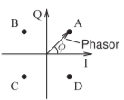
Figure \(\PageIndex{1}\): Phasor diagram with four discrete phase states that can be set by combining \(I\) and \(Q\) signals.
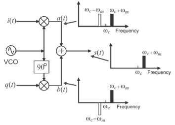
Figure \(\PageIndex{2}\): Quadrature modulator showing intermediate spectra.
So, in most digital modulation schemes, setting the amplitude and phase of a carrier addresses a point on a phasor diagram. A phasor diagram with four discrete states is shown in Figure \(\PageIndex{1}\). The circuit that implements this digital modulation is shown in Figure 3.4.6.
3.6.2 Quadrature Modulation
Quadrature modulation describes the frequency conversion process in which the real and imaginary parts of the RF phasor are varied separately. A subsystem that implements quadrature modulation is shown in Figure \(\PageIndex{2}\). This is quite an ingenious circuit. The operation of this subsystem is described by what is known as the generalized quadrature modulation equation:
\[\label{eq:1}s(t)=i(t)\cos[\omega_{c}t+\varphi_{i}(t)]+q(t)\sin[\omega_{c}t+\varphi_{q}(t)] \]
where, \(i(t)\) and \(q(t)\) embody the particular modulation rule for amplitude, \(\varphi_{i}(t)\) and \(\varphi_{q}(t)\) embody the particular modulation rule for phase, and \(\omega_{c}\) is the carrier radian frequency. In terms of the signals identified in Figure \(\PageIndex{2}\), the quadrature modulation equation can be written as
\[\begin{align}\label{eq:2}s(t)&=a(t)+b(t) \\ \label{eq:3}a(t)&=i(t)\cos[\omega_{c}t+\varphi_{i}(t)] \\ \label{eq:4}b(t)&=q(t)\sin[\omega_{c}t+\varphi_{q}(t)]\end{align} \]
Figure \(\PageIndex{2}\) shows that both \(a(t)\) and \(b(t)\) have two bands, one above and one below the frequency of the carrier, \(\omega_{c}\). However, there is a difference. The LO (here designated as the VCO) is shifted \(90^{\circ}\) (perhaps using an RC delay line) so that the frequency components of \(b(t)\) have a different phase relationship to the carrier than those of \(a(t)\). When \(a(t)\) and \(b(t)\) are combined, the carrier content is canceled, as is one of the sidebands provided that \(q(t)\) is a \(90^{\circ}\) phase-shifted version of \(i(t)\). This is exactly what is desired: the carrier should not be transmitted, as it contains no information. Also, it is desirable to transmit only one sideband, as it contains all of the information in the modulating signal. This type of modulation is SSB-SC modulation. In the next section, frequency modulation is used to demonstrate SSB-SC operation.
3.6.3 Frequency Modulation
Frequency modulation is considered here to demonstrate SSB-SC operation. Let \(i(t)\) and \(q(t)\) be finite bandwidth signals centered at radian frequency \(\omega_{m}\) with their phases \(\varphi_{i}(t)\) and \(\varphi_{q}(t)\) chosen so that \((\varphi_{q}(t) −\varphi_{i}(t))\) is \(90^{\circ}\) on average. This is shown in Figure \(\PageIndex{2}\), where \(\omega_{m}\) represents the frequency components of \(i(t)\) and \(q(t)\). With reference to Figure \(\PageIndex{2}\),
\[\label{eq:5}i(t)=\cos(\omega_{m}t)\quad\text{and}\quad q(t)=-\sin(\omega_{m}t) \]
and the general quadrature modulation equation, Equation \(\eqref{eq:1}\), becomes
\[\label{eq:6}s(t)=i(t)\cos(\omega_{c}t)+q(t)\sin(\omega_{c}t)=a(t)+b(t) \]
where
\[\label{eq:7}a(t)=\frac{1}{2}\{\cos[(\omega_{c}-\omega_{m})t]+\cos[(\omega_{c}+\omega_{m})t]\} \]
and
\[\label{eq:8}b(t)=\frac{1}{2}\{\cos[(\omega_{c}+\omega_{m})t]-\cos[(\omega_{c}-\omega_{m})t]\} \]
Thus the combined frequency modulated signal at the output is
\[\label{eq:9}s(t)=a(t)+b(t)=\cos[(\omega_{c}+\omega_{m})t] \]
and the carrier and lower sideband are both suppressed. The lower sideband, \(\cos[(\omega_{c}−\omega_{m})t]\), is also referred to as the image which may not be exactly zero because of circuit imperfections. In modulators it is important to suppress this image, and in demodulators it is important that undesired signals at the image frequency not be converted along with the desired signals.
3.6.4 Polar Modulation
In polar modulation, the \(i(t)\) and \(q(t)\) quadrature signals are converted to polar form as amplitude \(A(t)\) and phase \(\phi (t)\) components. This is either done in the DSP unit or, if a modulated RF carrier is all that is provided, using an envelope detector to extract \(A(t)\) and a limiter to extract the phase information corresponding to \(\phi (t)\). Two polar modulator architectures are shown in Figure 3.7.1. In the first architecture, Figure 3.7.1(a), \(A(t)\) and \(\phi (t)\) are available and \(A(t)\) is used to amplitude modulate the RF carrier, which is then amplified by a power amplifier (PA). The phase signal, \(\phi (t)\), is the input to a phase modulator implemented as a PLL. The output of the PLL is fed to an efficient amplifier operating near saturation (also called a saturating amplifier). The outputs of the two amplifiers are combined to obtain the large modulated RF signal to be transmitted.
In the second polar modulation architecture, Figure 3.7.1(b), a lowpower modulated RF signal is decomposed into its amplitude- and phasemodulated components. The phase component, \(\phi (t)\), is extracted using a limiter that produces a pulse-like waveform with the same zero crossings as the modulated RF signal. Thus the phase of the RF signal is captured. This is then fed to a saturating amplifier whose gain is controlled by the carrier envelope, or \(A(t)\). Specifically, \(A(t)\) is extracted using an envelope detector, with a simple implementation being a rectifier followed by a lowpass filter with a corner frequency equal to the bandwidth of the modulation. \(A(t)\) then drives a switching (and hence efficient) power supply that drives the saturating power amplifier.