
3.7: Case Study- SDR Transmitter
- Page ID
- 41193

An SDR transmitter combines DSB-SC modulation having a relatively low intermediate frequency carrier with a broadband analog SSB-SC modulation to produce a DSB-SC RF signal. There are many possible implementations. This case study presents system simulations of an SDR transmitter with specific parameters. First a DSB-SC quadrature modulator is studied with sinusoidal in-phase and quadrature baseband signals and then a SSB-SC modulator is examined. This is followed by the study of a direct analog modulation of a digital signal. The final study corresponds to a typical SDR transmitter with DSP-based intermediate frequency DSB-SC modulation followed by SSB-SC analog modulation producing a DSB-SC modulated RF signal.
3.10.1 Analog Quadrature Modulator
The quadrature modulator of Figure 3.9.1(a) is simulated here with a \(10\text{ MHz}\) sinewave for \(i(t)\), a \(15\text{ MHz}\) sinewave for \(q(t)\), and a \(1\text{ GHz}\) sinewave LO. The local oscillator is a \(1\text{ GHz}\) sinewave. The resulting RF waveform at the
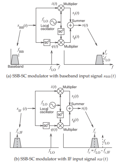
Figure \(\PageIndex{1}\): Quadrature modulator with the \(i(t)\) component derived directly from the input signal and \(q(t)\) derived from a \(90^{\circ}\) negatively phase-shifted input signal. The IF signal in (b) is typically a DSB-SC signal with intermediate carrier frequency \(f_{c,\text{ IF}}\) set in DSP.
output, \(s(t)\), is shown in Figure \(\PageIndex{2}\). The waveform is plotted on a \(1\:\mu\text{s}\) scale so that there are \(10\) cycles of \(i(t)\) and \(15\) cycles of \(q(t)\) which are modulated on \(1,000\) cycles of the \(1\text{ GHz}\) RF carrier.
The spectra of the signals at the outputs of the two multipliers, i.e. of \(s_{i}(t)\) and \(s_{q}(t)\), are shown in Figure \(\PageIndex{3}\)(a). Each spectrum has two peaks offset from the \(1\text{ GHz}\) LO frequency by \(10\text{ MHz}\) for the \(I\) signal, \(s_{i}(t)\), and by \(15\text{ MHz}\) for the \(Q\) signal, \(s_{q}(t)\). The amplitudes of each spectra are symmetrical around the LO frequency but there is a difference in the phase of the Fourier transforms of \(s_{i}(t)\) and \(s_{q}(t)\). The phases of the Fourier transforms of the signals are shown in Figure \(\PageIndex{3}\)(b). The upper and lower sideband phases of the \(10\text{ MHz }I\) channel signal are equal but the phases of the upper and lower sidebands of the \(15\text{ MHz }Q\) channel signal differ by \(180^{\circ}\), i.e. the upper sideband of \(s_{q}(t)\) is the negative of the lower sideband of \(s_{q}(t)\). In contrast the phases of the upper and lower realized sidebands of \(s_{i}(t)\) are equal.
The amplitude and phase spectra of the combined signal, \(s(t) = s_{i}(t) + s_{q}(t)\), are shown in Figures \(\PageIndex{3}\)(c and d) and are as expected from combining the spectra of the components. The spectrum of \(s(t)\), consists of two pairs of peaks with the peaks of one pair being above and below the LO frequency by \(10\text{ MHz}\), and the peaks of the other pair being offset by \(15\text{ MHz}\). The components are in a lower sideband and an upper sideband and hence this modulation is DSB modulation. Also there is not a component of the output signal at the local oscillator frequency, \(f_{\text{LO}}\). The middle of the output signal bandwidth is generally the carrier frequency \(f_{c}\) which here is the same as \(f_{\text{LO}}\). Thus the carrier does not exist in the output and so this is called suppressed carrier (SC) modulation. Together this is double sideband suppressed carrier (DSB-SC) modulation. Suppression of the carrier is a property of the multiplicative mixer but some types of modulators, e.g. amplitude modulators, have the carrier in the RF output signal and hence the suppressed-carrier distinction being used with quadrature modulation.
Note that each of the sidebands of the DSB-SC modulated signal have both \(I\) and \(Q\) information. With finite and equal bandwidth \(i(t)\) and \(q(t)\) signals, the \(I\) and \(Q\) information in the RF modulated signal will have overlapping lower sideband and upper sideband. It is only possible to recover and separate the original \(i(t)\) and \(q(t)\) signals if both sidebands are used in demodulation.
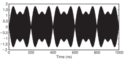
Figure \(\PageIndex{2}\): A \(1\text{ GHz}\) carrier modulated by a \(10\text{ MHz}\) sinusoidal \(i(t)\) and a \(15\text{ MHz}\) sinusoidal \(q(t)\).
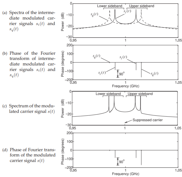
Figure \(\PageIndex{3}\): Spectrum of signals in the quadrature modulator of Figure \(\PageIndex{1}\)(a) with \(10\text{ MHz}\) in phase, \(i(t)\), and \(15\text{ MHz}\) quadrature-phase, \(q(t)\), modulating signals. (Simulated time \(= 65.536\:\mu\text{s}\), using a \(223\) point FFT.)
3.10.2 Single-Sideband Suppressed-Carrier (SSB-SC) Modulation
Examination of the phase differences of the lower and upper sideband components with the DSB-SC modulator considered in the previous section leads to the design of a SSB-SC modulator. This is obtained when \(i(t)\) and \(q(t)\) are the same signal except that the frequency components of \(q(t)\) lag those of \(i(t)\) by \(90^{\circ}\). Thus the phase components of \(s_{q}(t)\) shown in Figure \(\PageIndex{3}\)(b) are shifted by \(−90^{\circ}\) so that the lower sideband components of \(s_{i}(t)\) and \(s_{q}(t)\) (now having the same frequency) combine constructively but the upper sideband components cancel. The variation of the quadrature modulator that implements this is shown in Figure \(\PageIndex{4}\)(a) with the baseband signal
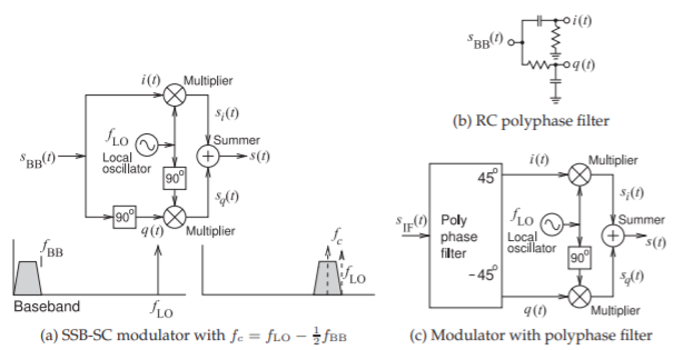
Figure \(\PageIndex{4}\): Quadrature modulator as a single-sideband, suppressed-carrier (SSB-SC) modulator. At the design frequency the polyphase filter in (b) the phase of \(i(t)\) is advanced by \(45^{\circ}\) and the phase of \(q(t)\) is retarded by \(45^{\circ}\).
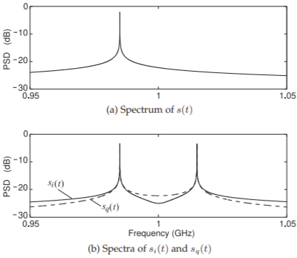
Figure \(\PageIndex{5}\): Spectra of the modulated signal with \(f_{\text{LO}} = 1\text{ GHz}\). (Simulated time \(= 65.536\:\mu\text{s},\: 223\) point FFT.)
\(s_{\text{BB}}(t) = i(t)\), and \(q(t)\) is the same signal except that \(q(t)\) lags \(i(t)\) by \(90^{\circ}\). The signals in this modulator will now be examined.
With \(s_{\text{BB}} = i(t)\) being a \(15\text{ MHz}\) sinusoidal signal, the \(q(t)\) is a \(15\text{ MHz}\) sinewave that lags \(i(t)\) by \(90^{\circ}\). The spectrum at the output of the quadrature modulator of Figure \(\PageIndex{4}\)(a and c) is as shown in Figure \(\PageIndex{5}\)(a). Now there is only one sideband. Insight into the operation of SSB modulation is obtained by examining the spectra of the signals at the output of the multipliers, see Figure \(\PageIndex{5}\)(b). It is seen that the amplitude spectra of \(s_{i}(t)\) and of \(s_{q}(t)\) are
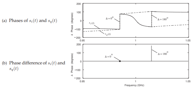
Figure \(\PageIndex{6}\): Phase of the modulated signal. (Simulated time \(= 65.536\:\mu\text{s},\: 223\) point FFT.)
essentially the same and both have upper and lower sidebands. However there is a difference in the phases of their Fourier transforms, see Figure \(\PageIndex{6}\). It is seen that at \(15\text{ MHz}\) offset from the \(1\text{ GHz}\) LO there is no differences in the phases of \(s_{i}(t)\) and \(s_{q}(t)\) components in the lower sideband but there is a \(180^{\circ}\) difference in the upper sideband, see Figure \(\PageIndex{6}\)(b). Thus when \(s_{i}(t)\) and \(s_{q}(t)\) are summed their lower sideband components add but their upper sideband components cancel thus suppressing the upper sideband in the combined signal \(s(t)\). This illustrates the most important metric of a SSB modulator as having I/Q paths that are matched as any imbalance in implementation that results in an amplitude or phase difference of the \(I\) and \(Q\) paths will result in a spurious (upper) sideband. Provided that the balance is good a filter is not required to suppress an upper sideband.
The SSB-SC modulator was modeled here with a sinusoidal input signal, \(s_{\text{BB}}(t)\), but upper sideband suppression will also be obtained with a finite bandwidth baseband signal. This is achieved if every frequency component of \(s_{\text{BB}}(t)\) is \(90^{\circ}\) phase-shifted to become \(q(t)\) so that \(q(t)\) is the quadraturephase version of the in-phase \(i(t)\). A circuit that implements this is the polyphase filter and one type is the RC circuit shown in Figure \(\PageIndex{4}\)(b). This has a finite bandwidth but this can be broadened by using multiple stages, e.g. see Figure 3.9.2(b). Incorporating the polyphase filter in the quadrature modulator leads to the implementation in Figure \(\PageIndex{4}\)(c).
3.10.3 Digital Quadrature Modulation
A digital quadrature modulator is shown in Figure \(\PageIndex{7}\). The input bitstream \(S_{k}\) is converted into two independent binary bitstreams \(I_{k}\) and \(Q_{k}\) which are then lowpass filtered, or in general wave-shaped, to provide two independent analog signals \(i(t)\) and \(q(t)\). That is, each pair of bits in the \(S_{k}\) bitstream becomes one \(I_{k}\) bit and one \(Q_{k}\) bit. The binary waveforms of \(I_{k}\) and \(Q_{k}\) are then filtered to obtain the analog signals \(i(t)\) and \(q(t)\) each of which has the same baseband bandwidth indicated in the spectrum on the lower
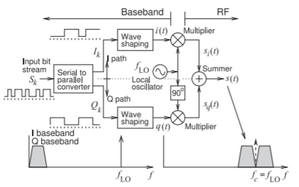
Figure \(\PageIndex{7}\): Digital quadrature modulators with independent binary I and Q channels yielding double sideband, suppressed carrier (DSB-SC) modulation.
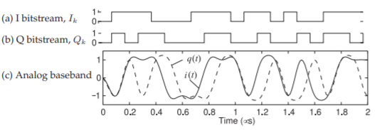
Figure \(\PageIndex{8}\): Baseband signals for a four state binary quadrature modulator. The \(I_{k}\) and \(Q_{k}\) bitstreams are derived from the random bitstream \(S_{k} = \mathsf{00 11 10 11 01 00 10 11 11 00 10 11 00 10 01 00 11 11 10}\) and taken as \((I_{k},Q_{k})\) pairs. The initial setting is \(i(0) = 0 = q(0)\).
left in Figure \(\PageIndex{7}\). The in-phase baseband signal, \(i(t)\), is multiplied by the local oscillator signal having frequency \(f_{\text{LO}}\). Also, the quadrature baseband signal, \(q(t)\), is multiplied by the local oscillator signal having frequency \(f_{\text{LO}}\) but now the LO is delayed by \(90^{\circ}\). Summing \(s_{i}(t)\) and \(s_{q}(t)\), the outputs of the multipliers, yields the double sideband suppressed carrier RF signal \(s(t)\) which has twice the bandwidth of each of the analog baseband signals as indicated in the lower right in Figure \(\PageIndex{7}\).
The modulator of Figure \(\PageIndex{7}\) results in four states of the modulated carrier signal. That is, if the modulated carrier signal \(s(t)\) is sampled at a time indicated by the common clock of \(I_{k}\) and \(Q_{k}\), the sample of the carrier will have a particular amplitude and phase. Since this is QPSK modulation the amplitudes at these multiple sampling instances will be the same but the phases will have four values addressed by the coordinate \((I_{k}, Q_{k})\).
Now consider a particular quadrature multiplier where \(S_{k}\) is a \(20\text{ Mbit/s}\) random bitstream so that \(I_{k}\) and \(Q_{k}\) are the \(10\text{ Mbit/s}\) bit streams shown in Figure \(\PageIndex{8}\)(a and b). The \(I_{k}\) and \(Q_{k}\) bitstreams are then level shifted so that the transitions are between \(−1\) and \(1\) instead of between \(0\) and \(1\). The level-shifted bitstreams are then lowpass filtered to obtain the analog baseband signals \(i(t)\) and \(q(t)\) shown in Figure \(\PageIndex{8}\)(c). The lowpass filter used here is a raised cosine filter which is commonly used in digital modulation rather than a lumped-element lowpass filter and here has an effective corner frequency
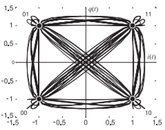
Figure \(\PageIndex{9}\): Constellation diagram for the binary quadrature modulator. This is also the phasor diagram (with appropriate scaling) of the modulated carrier signal with constellation points sampled at \(0.1\:\mu\text{m}\) intervals shown as large dots. There are four constellation points corresponding to four symbols and each symbol represents two bits of information.
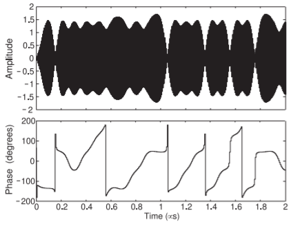
Figure \(\PageIndex{10}\): Amplitude and phase of the modulated carrier signal \(s(t)\) as the output of a binary modulator with a \(20\text{ Mbit/s}\) digital baseband signal. Note that the rapid phase transitions occur when the amplitude of the modulated carrier goes to zero. (The rapid switch between \(180^{\circ}\) and \(−180^{\circ}\) when the amplitude is not zero is a continuous smooth phase change.)
of \(7\text{ MHz}\). In practice the raised cosine filter is implemented in DSP so that the signals \(i(t)\) and \(q(t)\) follow DACs.
One feature of the raised cosine filter is that the filtered response at the clock-derived sampling times is exact. That is, if the filtered analog baseband signals are sampled every \(0.1\:\mu\text{s}\) then the sampled values of \(i(t)\) and \(q(t)\) will be exactly either \(+1.00\) or \(−1.00\) and (after level-shifting by adding one and multiplying by half) the original bitstream is exactly recovered as \(0\) or \(1\). If an analog lowpass filter was used the sampled values would not be exactly right. The raised cosine filter introduces no sampling distortion and also the transitions are minimal, i.e. they have the minimum bandwidth compared to what would be obtained if an analog filter was used for wave-shaping. The bandwidth of the filtered signal obtained using a lumped-element filter would be \(10\text{ MHz}\) or more and even then the carrier samples would never correspond exactly with the constellation points. Plotting \(q(t)\) against \(i(t)\) yields the transitions shown in Figure \(\PageIndex{9}\). Samples of the baseband signal every \(0.1\:\mu\text{s}\) coincides with one of the four states and enables two bits of information to be recovered.
The next stage of the DSB-SC modulator multiplies the \(i(t)\) signal by a \(1\text{ GHz}\) LO and the \(q(t)\) signal is multiplied by a \(90^{\circ}\) phase-shifted LO. Then the outputs of the multipliers are summed to produce the modulated RF signal \(s(t)\) shown in Figure \(\PageIndex{10}\). The LO here is in the middle of the RF bandwidth and so here the carrier frequency is the same as the LO frequency.
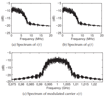
Figure \(\PageIndex{11}\): Spectra of signals in the digital modulator with a \(20\text{ Mbit/s}\) input stream, \(S_{k}\), and a \(1\text{ GHz}\) LO. (\(1024\) symbols, a time duration of \(102.4\:\mu\text{s}\), and using a \(524,288\) point FFT)
Sampling the RF signal \(s(t)\) every \(0.1\:\mu\text{s}\) provides the amplitudes and phases of the carrier with each sample coinciding with one of the constellation points. This modulation scheme is generally called QPSK modulation for quadra-phase shift keying but it is sometimes, but less accurately, called quadrature phase shift keying. In QPSK modulation each constellation point corresponds to one of four phases of the RF signal: \(45^{\circ},\: 135^{\circ},\: −45^{\circ},\) or \(−135^{\circ}\).
QPSK modulation was originally implemented with simpler hardware so the QPSK term is used rather than 4-QAM for four-state quadrature amplitude modulation which more accurately reflects the modulation process described in this section, it does not have to be done this way if only the phase of the carrier is to be adjusted.
Plotting the phasor of the RF carrier signal will result in a phasor diagram identical to the transitions shown in the constellation diagram of Figure \(\PageIndex{9}\) although it may be necessary to scale the amplitude of the phasor signal to match the values in the constellation diagram. Note that the constellation diagram does not change when the average signal level changes. With the sampling clock aligned to the original clock for the \(I_{k}\) and \(Q_{k}\) bitstreams, samples of the RF phasor will precisely coincide with one of the constellation points in Figure \(\PageIndex{9}\) (and hence \(s(t)\) is on the way to being demodulated).
Digital radio sends data in finite length packets and here the packet is \(2048\) bits long. With \(2\) bits per symbol in QPSK modulation there are \(1024\) symbols and with a symbol interval of \(0.1\:\mu\text{s}\), the duration of the packet is \(102.4\:\mu\text{s}\).
The spectra of the baseband and the output RF signals in the modulator are shown in Figure \(\PageIndex{11}\). The spectra of \(i(t)\) and \(q(t)\), Figures \(\PageIndex{11}\)(a and b) respectively, are not identical because each bitstreams is independent. For each bitstream the spectra extends down to DC. It would be possible to use a coding scheme for the bitstreams that ensures that there is not a DC component and this aids automatic carrier recovery in pre-4G cellular systems. Instead 4G and 5G systems use separate mechanisms enabling carrier recovery. The bandwidth of the in-phase and quadrature-phase
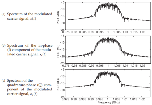
Figure \(\PageIndex{12}\): Spectra of the digitally modulated RF signals for \(1024\) symbols (\(4096\) bits), a time duration of \(102.4\:\mu\text{s}\), and using a \(524,288\) point FFT.
analog baseband signals are slightly less than \(10\text{ MHz}\). The spectrum of the RF output signal is shown in Figure \(\PageIndex{11}\)(c) and the bandwidth of this double-sideband modulated signal is slightly less than \(20\text{ MHz}\). The RF signal has two sidebands, one below \(1\text{ GHz}\) and one above even though there is no clear demarcation such as a dip at \(1\text{ GHz}\). The continuous spectrum through \(1\text{ GHz}\) is a consequence of the baseband spectra extending to DC.
As was noted previously, and in the absence of noise, the constellation points are faithfully replicated if the RF signal is sampled at \(0.1\:\mu\text{s}\) intervals (provided that the phase and the frequency of the carrier has been replicated accurately). The replication of the constellation points is a property of the raised cosine filter which also results in reduced bandwidth baseband analog signals than would be obtained if analog lowpass filtering was used. Also note that (with the DSB-SC quadrature modulation described here) the carrier frequency, the center of the RF signal spectrum, is \(1\text{ GHz}\), the same as the LO frequency.
The spectra of all of the RF signals are shown in Figure \(\PageIndex{12}\). The spectrum of the RF output, Figure \(\PageIndex{12}\)(a), is centered at \(1\text{ GHz}\) and this is the carrier frequency and is also the LO frequency for this DSB-SC transmitter. A curiosity is examining the phases of the RF signals, however little insight is obtained from the phase plots in Figure \(\PageIndex{13}\).
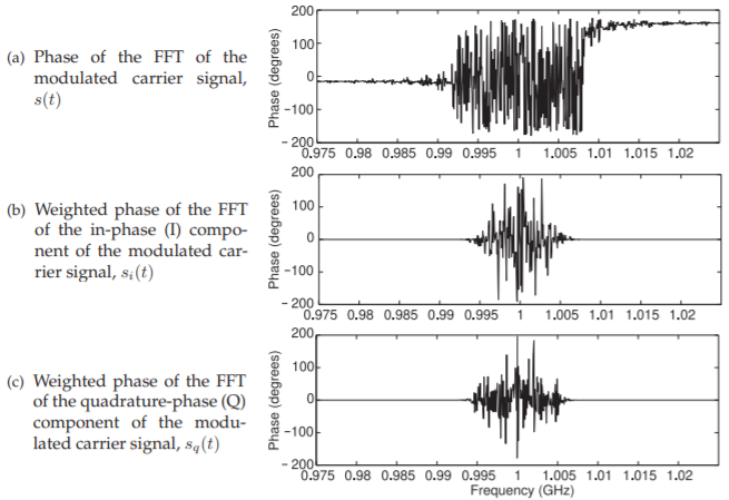
Figure \(\PageIndex{13}\): Phase of the FFT of the digitally modulated RF signal and its components. The phase of the \(s_{i}(t)\) and \(s_{q}(t)\) has been weighted by their spectrum amplitudes as otherwise meaningless numerical noise dominates the plots outside the passband. (Using \(1024\) symbols, \(102.4\:\mu\text{s}\))
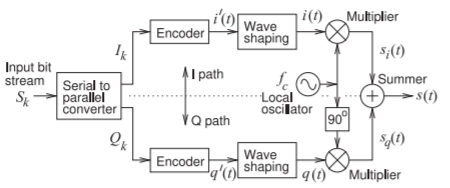
Figure \(\PageIndex{14}\): High-order digital quadrature modulator with independent I and Q paths yielding double sideband, suppressed carrier (DSB-SC) modulation.
3.10.4 QAM Digital Modulation
The QPSK digital modulator considered in the previous section had only four states. This is a consequence of the digital baseband bitstreams, \(I_{k}\) and \(Q_{k}\), being used one bit at a time. If two or more bits are used at a time to address a constellation point, more data can be sent in the same RF bandwidth. Modulation that does this is called higher-order digital modulation. A higher-order quadrature modulator is shown in Figure \(\PageIndex{14}\) where now groups of two or more \(I_{k}\) bits and \(Q_{k}\) bits can be encoded as an analog signal. That is, if there are four possible values of \(i(t)\) at the clock ticks, then pairs of \(I_{k}\) bits are encoded as one of four analog values. Such as the \(I_{k}\)
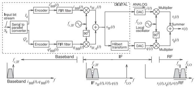
Figure \(\PageIndex{15}\): Complete SDR transmitter with bistream \(S_{k}\) input to an IF quadrature modulator producing a DSB-SC signal, \(s_{\text{IF}}\), with IF carrier of frequency \(f_{c,\text{ IF}}\). Each finite-impulse response (FIR) filter implements raised cosine filtering. Then an analog SSB-SC quadrature modulator upconverts the IF as a DSB-SC RF signal centered at the RF carrier frequency \(f_{c} = f_{\text{LO}} − f_{c,\text{ IF}}\). The Hilbert transform implements a \(90^{\circ}\) phase shift.
bit pair \(\mathsf{00}\) resulting in \(i(t)\) before filtering, i.e. \(i′ (t)\), being encoded as \(−1\text{ V}\), \(\mathsf{01}\) being encoded as \(−\frac{1}{3}\text{ V}\), \(\mathsf{10}\) being encoded as \(+\frac{1}{3}\text{ V}\), and \(\mathsf{11}\) being encoded as \(+1\text{ V}\). \(Q_{k}\) would be encoded the same way. This results in \(16\) possible states and this is called 16-QAM modulation. Operation of this quadrature modulator will be analyzed in the next section in the context of a complete SDR transmitter.
3.10.5 SDR Transmitter Using QAM Digital Modulation
This section describes a 16-QAM modulator as used in modern communications systems (4G and 5G). This reflects the capabilities of baseband DSPs which can perform many of the modulation operations. The architecture of a QAM quadrature-modulator is depicted in block diagram form in Figure \(\PageIndex{5}\). This modulator consists of two quadrature modulators, a DSP-based digital IF quadrature modulator on the left, and an analog RF quadrature modulator on the right. The digital IF quadrature modulator on the left is a DSB-SC quadrature modulator taking an input bitstream and partitioning it by converting from a serial input bit stream, \(S_{k}\), into two parallel but independent bitstreams, \(I_{k}\) and \(Q_{k}\). The output of the IF quadrature modulator, \(s_{\text{IF}}(t)\), is a DSB-SC IF signal centered at the IF carrier frequency \(f_{c,\text{ IF}}\). This is then modulated by the analog RF quadrature modulator to create a SSB-SC RF signal which has the IF signal, \(s_{\text{IF}}(t)\), as its modulating signal. The RF signal however retains the double sidebands of the IF signal so that \(s(t)\) is a DSB-SC signal with carrier frequency \(f_{c} = f_{\text{LO}} − f_{c,\text {IF}}\).
The 16-QAM system has the parameters given in Table \(\PageIndex{1}\). Since pairs of \(I_{k}\) bits and pairs of \(Q_{k}\) bits are used to encode the baseband analog signals \(i_{\text{BB}}′\) and \(q_{\text{BB}}′\) there are \(16\) possible states and 16-QAM modulation is the result. The constellation diagram of 16-QAM modulation is shown in
| Input bitstream \(S_{k}\) | \(40\text{ Mbit/s}\) | ||
| \(I_{k}\) bitstream | \(20\text{ Mbit/s}\) | ||
| \(Q_{k}\) bitstream | \(20\text{ Mbit/s}\) | ||
| Nominal bandwidth \(i_{\text{BB}}'\) | \(10\text{ MHZ}\) (discrete) | Bandwidth \(i(t)\) | \(20\text{ MHZ}\) (analog) |
| Nominal bandwidth \(q_{\text{BB}}'\) | \(10\text{ MHZ}\) (discrete) | Bandwidth \(q(t)\) | \(20\text{ MHz}\) (analog) |
| Intermediate carrier, \(f_{c,\text{ IF}}\) | \(10\text{ MHZ}\) (discrete) | Local oscillator, \(f_{\text{LO}}\) | \(1\text{ GHz}\) |
| Nominal bandwidth \(s_{\text{IF, }i}\) | \(20\text{ MHZ}\) (discrete) | Bandwidth \(s_{i}(t)\) | \(20\text{ MHz}\) (analog) |
| Nominal bandwidth \(s_{\text{IF, }q}\) | \(20\text{ MHZ}\) (discrete) | Bandwidth \(s_{q}(t)\) | \(20\text{ MHz}\) (analog) |
| Nominal bandwidth \(s_{\text{IF}}\) | \(20\text{ MHZ}\) (discrete) | Bandwidth \(s(t)\) | \(20\text{ MHz}\) (analog) |
| IF carrier, \(f_{c,\text{ RF}}\) | \(10\text{ MHZ}\) | RF carrier, \(f_{c,\text{ RF}}\) | \(990\text{ MHz}\) |
Table \(\PageIndex{1}\): Parameters of the SDR transmitter considered in Section 3.10.4.
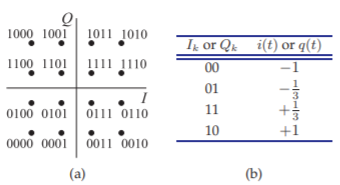
Figure \(\PageIndex{16}\): 16-QAM modulation: (a) constellation diagram; and (b) table translating binary value of \(I\) (or \(Q\)) to an absolute value \(i(t)\) (or \(q(t)\)).
Figure \(\PageIndex{16}\)(a) with the bit-wise addresses of the constellation points. There are \(16\) constellation points each of which indicates a symbol which provides four bits of information. In the case of QAM modulation the constellation diagram corresponds to a phasor diagram with each constellation point indicating the amplitude and phase of the RF signal at a point in time. The difference between the constellation diagram and a phasor diagram is that the constellation diagram does not change when the average power of the RF signal changes. Thus the constellation diagram of QAM corresponds to a phasor diagram that is continuously being re-normalized to the average RF power.
The table in Figure \(\PageIndex{16}\)(b) shows the encoding that enables pairs of \(I_{k}\) bits and pairs of \(Q_{k}\) bits to address a symbol in the constellation diagram. That is, each of these bitstreams is encoded so that two bits are encoded as one analog value. Figure \(\PageIndex{17}\)(a) shows the bits in the input bitstream, \(S_{k}\), which are in groups of four bits with the first and third bits of the group becoming I bits and the second and fourth bits in the group becoming Q bits. The \(I_{k}\) and \(Q_{k}\) bitstreams are shown in Figures \(\PageIndex{17}\)(b) and \(\PageIndex{17}\)(c) respectively. A pair of \(I_{k} (Q_{k})\) bits yields an encoded \(i_{\text{BB}}′ (q_{\text{BB}}′)\) value every \(0.1\:\mu\text{s}\). Here \(I_{k} = I_{1}I_{2}I_{3}I_{4}I_{5}I_{6} = \mathsf{011100}\) so \(i′ (0.1\:\mu\text{s}) = −\frac{1}{3}, i′ (0.2\:\mu\text{s}) = +\frac{1}{3}\), and \(i′ (0.3\:\mu\text{s}) = −1\). Linearly interpolating these yields the \(i_{\text{BB}}′\) and \(q_{\text{BB}}′\) waveforms shown in Figure \(\PageIndex{17}\)(d). In DSP of course these are discrete values but have been plotted as continuous waveforms which is more easily visualized.
FIR filtering of \(i_{\text{BB}}′\) and \(q_{\text{BB}}′\) yields the band-limited waveforms \(i(t)\) and \(q(t)\) shown in Figure \(\PageIndex{17}\)(e). Filtering introduces a delay and here the delay is \(0.2\:\mu\text{s}\). Thus the first encoded value before filtering is established at \(0.1\:\mu\text{s}\), see
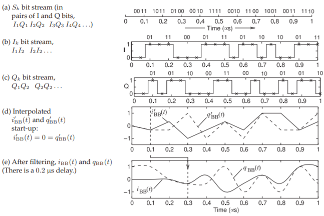
Figure \(\PageIndex{17}\): Baseband signals for 16-QAM modulation with markers showing the baseband bit impulse times. The bit pairs shown above each bit waveform \(0.1\:\mu\text{s}\) intervals.
the vertical dashed line in Figure \(\PageIndex{17}\)(d), and the first symbol (represented by \(i_{\text{BB}}\) and \(q_{\text{BB}}\)) is at \(0.3\:\mu\text{s}\), see the vertical dashed line in Figure \(\PageIndex{17}\)(e). The baseband values are actually discrete samples. With an oversampling factor of \(8\), the \(i_{\text{BB}}′\) samples, the interpolated encoded values, are as shown in Figure \(\PageIndex{18}\)(b) and the interpolated \(q_{\text{BB}}′\) samples in Figure \(\PageIndex{18}\)(d). In this SDR transmitter baseband filtering is a raised cosine filter implemented digitally as a finite impulse response (FIR) filter.
The interpolated encoded samples \(i_{\text{BB}}′\) and \(q_{\text{BB}}′\) are filtered digitally using a finite impulse response (FIR) filter yielding the filtered samples \(i_{\text{BB}}\) and \(q_{\text{BB}}\) shown in Figures \(\PageIndex{8}\)(c and e) respectively. The raised-cosine FIR filter has a span of \(4\) symbols (i.e. \(0.4\:\mu\text{s}\)) and since the oversampling factor is \(8\) the FIR filter’s response is \(33\) samples long, see Figure \(\PageIndex{18}\)(a). (With the \(0\)th and \(33\)rd bins being zero, it could be said to be \(31\) or \(32\) samples long.) (Specification of the raised cosine filter filter is completed with a roll-off factor of \(0.7\) which describes how quickly the impulse response rolls-off around its peak response.) The peak response of the filter is at the \(16\)th sample, after \(0.2\:\mu\text{s}\), and the impulse responses at \(0 (−0.2\:\mu\text{s}), 8 (−0.1\:\mu\text{s}), 24 (0.1\:\mu\text{s}),\) and \(32 (0.2\:\mu\text{s})\) samples are zero. Thus the FIR filter introduces a \(0.2\:\mu\text{s}\) delay. There are other types of FIR filters including two-dimensional FIR filters that operate on the I and Q channels together and can provide even better management of the bandwidth of the modulated IF signal.
The next stage in the transmitter is multiplying \(i_{\text{BB}}\) by the IF LO having
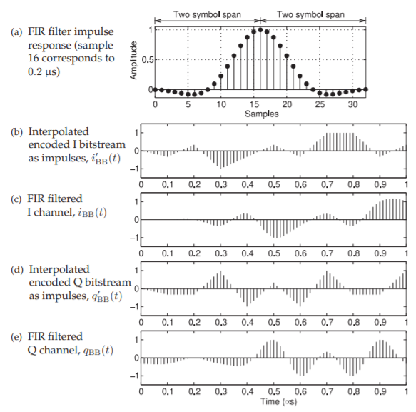
Figure \(\PageIndex{18}\): Sampled baseband signals for 16-QAM modulation corresponding to the analog baseband signals in Figure \(\PageIndex{17}\).
frequency \(f_{c,\text{ IF}}\) and multiplying \(q_{\text{BB}}\) by a \(90^{\circ}\) phase-shifted IF LO. This results in the modulated IF signal, \(s_{\text{IF}}\), shown in Figure \(\PageIndex{19}\)(a).
The procedure of producing a SSB-SC modulated RF signal from the IF signal is to drive the multipliers in the RF quadrature modulator of the second mixing stage with an in-phase IF signal and its quadrature, i.e. \(90^{\circ}\) phase-shifted version. In this case every frequency component of \(s_{\text{IF}}\) must be phase shifted by \(90^{\circ}\). The mathematical procedure that does this is the Hilbert transform operating on a finite number of samples of \(s_{\text{IF}}\) and here \(8192\) symbols with an oversampling factor of \(8\) were considered so that the Hilbert transform operates on \(65,536\) samples. In DSP an FFT can be used so that an FFT of \(s_{\text{IF}}\) yields the amplitude and phase of discrete frequency components of \(s_{\text{IF}}\) and then the individual frequency samples are phase-shifted by \(90^{\circ}\). Then an inverse FFT yields the required Hilbert transform in the time domain. A DAC then converts the digital samples into the analog signals \(i(t)\) and \(q(t)\). Their waveforms are shown in Figures \(\PageIndex{19}\)(a and b).
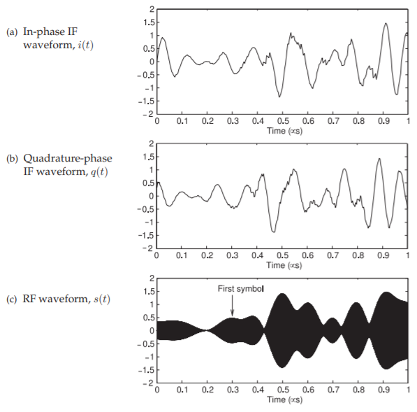
Figure \(\PageIndex{19}\): Waveforms in the RF quadrature modulator where the in-phase IF signal \(i(t)\) is just the output, \(s_{\text{IF}}(t)\) of the IF quadrature multiplier. The first \(0.2\:\mu\text{s}\) can be ignored as the FIR filter output is settling. (The IF sampling interval is \(3.125\text{ ns}\). The Hilbert transform operates on \(2^{16} =65,537\) IF samples or \(204.8\:\mu\text{s}\) of data corresponding to \(2048\) symbols or \(8192\) bits. The RF time step is \(31.25\text{ ps}\). The RF signal spectrum was calculated using a \(2^{22}\) point FFT.
Then these signals are quadrature modulated using an RF LO of \(1\text{ GHz}\) yielding the RF waveform shown in Figure \(\PageIndex{19}\)(c). The SSB-SC RF analog modulator has translated the DSB-SC IF signal to RF to produce a DSB-SC RF signal. Plots of \(i(t),\: q(t)\) and \(s(t)\) over a longer time are shown in Figure \(\PageIndex{20}\).
The spectra of the IF and RF signals are shown in Figure \(\PageIndex{20}\). It is seen that the bandwidth of the IF modulated signal is just under \(20\text{ MHz}\) and the bandwidth of the RF signal is the same. The carrier of the IF signal is \(10\text{ MHz}\), the center of the DSB-SC modulated IF. The RF signal is centered around \(990\text{ MHz}\) and this is the carrier frequency of the radio signal. That is the \(10\text{ MHz}\) carrier frequency, \(f_{c,\text{ IF}}\) has been up-converted to the lower
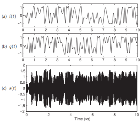
Figure \(\PageIndex{20}\): In-phase and quadrature-phase waveforms and RF waveforms in the RF quadrature modulator.
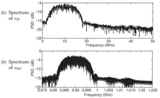
Figure \(\PageIndex{21}\): Spectrum of the IF and RF modulated carriers.
sideband of the \(1\text{ GHz}\) LO.
The constellation diagram together with trajectories of the modulated carrier signal are shown in Figure \(\PageIndex{22}\) for various numbers of symbols. This also corresponds to the phasor diagram of the QAM modulated signal except that the constellation diagram is effectively a phasor diagram that is re-normalized to the average power level so that the constellation diagram does not change with the average RF power changes. A phasor diagram would change of course as the average RF power changed. The trajectories in Figure \(\PageIndex{22}\) go through a constellation point every \(0.1\:\mu\text{s}\). So provided that
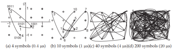
Figure \(\PageIndex{22}\): Constellation diagram with trajectories of the phasor of \(f_{c}\) for various symbol lengths with the first symbol at \(0.3\:\mu\text{s}\). Each symbol has \(4\) bits. In (a) and (b) the first symbol is labeled ’\(\mathsf{1}\)’, etc.
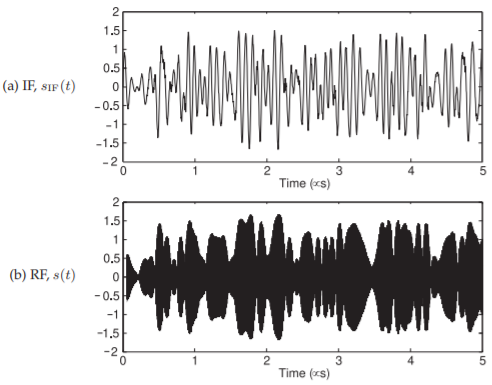
Figure \(\PageIndex{23}\): Comparison of the IF and RF modulated signals.
the clock in a receiver is correctly aligned and samples the RF signal every \(0.1\:\mu\text{s}\), the transmitted symbols will be precisely recovered. This of course is in the absence of noise and circuit non-idealities.
The transmitter described here has two modulation stages. The IF quadrature modulator modulates the baseband signal as a DSB-SC IF signal with a bandwidth of around \(20\text{ MHz}\) on a \(10\text{ MHz}\) carrier. The second stage, the RF quadrature modulator, takes the IF waveform and SSB-SC modulates it on a \(990\text{ MHz}\) carrier and maintains the IF bandwidth. The relationship between the IF and RF waveforms is easier to see by viewing the waveforms over a \(5\:\mu\text{s}\) span corresponding to \(50\) cycles of the \(10\text{ MHz}\) IF carrier and approximately \(5000\) cycles of the RF LO (and \(5051\) cycles of the RF carrier), see Figure \(\PageIndex{23}\).
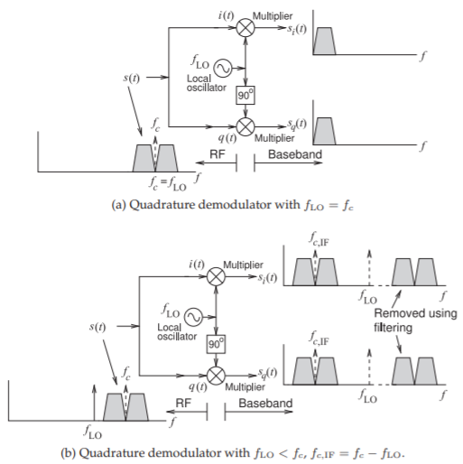
Figure \(\PageIndex{24}\): Quadrature demodulators used to down-convert an I/Q modulated RF signal.
Summary
The SDR transmitter involves many technologies. This interplay was best demonstrated using the specific parameters of the SDR transmitter considered in this section. The main limitation is on the bandwidth of the IF modulated signal as this relates directly to the performance of the DSP unit which in turn impacts battery drain. The advantages of implementing a first stage using DSP are tremendous and nearly any modulation scheme can be supported simply by changing the parameters in the DSP unit. The analog RF unit can support very wide bandwidths as fixed frequency filters are not needed. The most critical performance parameter is balancing the I and Q paths through the entire transmitter chain. With most of the modulation occurring in the DSP unit, balancing of the digital portions of the I and Q paths is achieved precisely. The challenge then falls to balancing the I and Q paths in the analog RF modulator.