
3.3: Case Study- Analysis of a Distributed Amplifier
- Page ID
- 46036
Figure \(\PageIndex{1}\)(a) shows the layout of a monolithically integrated, large signal, distributed, GaAs power amplifier [4], model TGA8220 from Texas Instruments. The schematic of the amplifier is shown in Figure \(\PageIndex{1}\)(b). This amplifier circuit is designed to deliver \(+25\text{ dBm}\) output power at \(1\text{ dB}\) compression when operating from \(2–18\text{ GHz}\). Identical FETs are used in
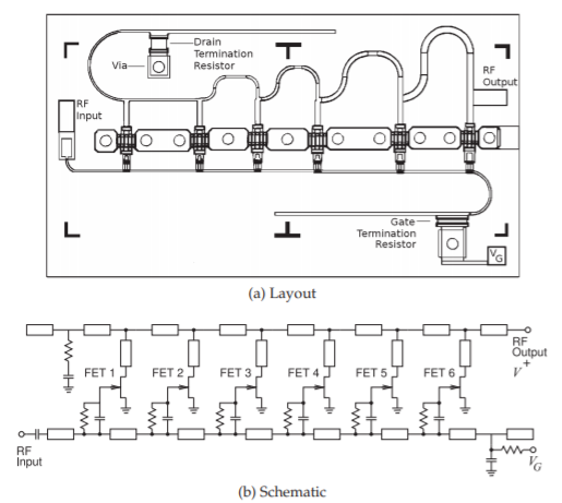
Figure \(\PageIndex{1}\): The TGA8220 MMIC distributed amplifier with six FETs (numbered 1–6 from the RF input). After [4], copyright Microwaves & RF, used with permission.
the six-stage amplifier and have a gate length \(L = 0.5\:\mu\text{m}\) and gate width \(W = 335\:\mu\text{m}\). Models of bends, tee junctions, vias, bond wires, and FET parasitics must be used. After bias and RF sources are defined, the circuit can be simulated in a nonlinear microwave simulator [5].
The small signal gain and the output power and efficiency at \(1\text{ dB}\) gain compression are shown in Figure \(\PageIndex{2}\) with \(V_{DS} = 8\text{ V}\) and \(50\%\) \(I_{DSS}\). The circuit was designed with series-gate capacitors to increase the gate-line cutoff frequency and to tailor the gate voltage excitation to maximize output power. Further gain and power enhancements were achieved with the help of tapered drain lines and a large drain termination resistor. This enables a \(1\text{ dB}\) compressed output power of \(+25\text{ dBm}\) with a power added efficiency of \(10\%\) to be obtained over the \(2–18\text{ GHz}\) band. The small-signal gain of at least \(19\text{ dB}\) also has a small positive slope with frequency.
Nonlinear circuit simulation can also be used to understand the intuitive operation of the nonlinear circuit. This is particularly important for complex circuits such as this one, which uses FETs that are increasingly loaded by distributing them in a systematic manner. One particularly useful form of display that aids in understanding is the I-V phase plane, which is the locus of the I-V trajectory of an individual device’s operating characteristic. The dynamic loadline of each FET in the amplifier at \(18\text{ GHz}\) for \(1\text{ dB}\) gain
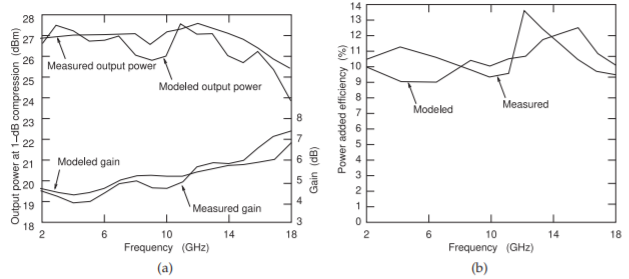
Figure \(\PageIndex{2}\): Gain, power, and efficiency of the TGA8220 MMIC distributed amplifier: (a) small-signal gain and output power at \(1\text{-dB}\) compression; and (b) efficiency at \(1\text{-dB}\) compression. After [4], copyright Microwaves & RF, used with permission.
compression at the output is given in Figure 3.4.1. The DC loadline (not shown) is a single line for each FET. The dynamic loadline opens up because of reactive loading. The match becomes better going from FET 1 to FET 6. Ideally the closed dynamic loadline would be achieved for all FETs, but there are many trade-offs required to achieve good gain, output power, and broad bandwidth. For efficiency, emphasis should be on maximizing the efficiency of the final stage, which operates at the highest power levels. The design here results in optimum output power across the entire bandwidth without unduly degrading the small-signal gain and input and output match for the remaining FETs in this amplifier. The use of series-gate capacitors and tapered drain lines is the mechanism that achieves this in this design [4]. A distributed amplifier delivers maximum output power and efficiency when each FET reaches gate and drain voltage limits for maximum power and efficiency simultaneously over a broad range of frequencies.