
3.4: Negative Image Amplifier Design
- Page ID
- 46037
Design using the negative image method is illustrated in the case study in Section 3.5 but here the philosophy behind the technique will be explained. The method breaks the stages the design in to much simpler steps.
In this section wideband amplifier design using the negative image method will be described for an amplifier having a single transistor. The idea can be applied to amplifier designs with multiple transistors. The basic model of a microwave transistor has shunt input and output capacitances and a feedback capacitance between the output and the input. A good amplifier design strategy would be to first place (ideal) negative capacitances in shunt with each of these capacitors and then attempt to synthesize a circuit that looks like a negative capacitor. This describes the essence of the negative image amplifier design method except that no attempt is made to directly
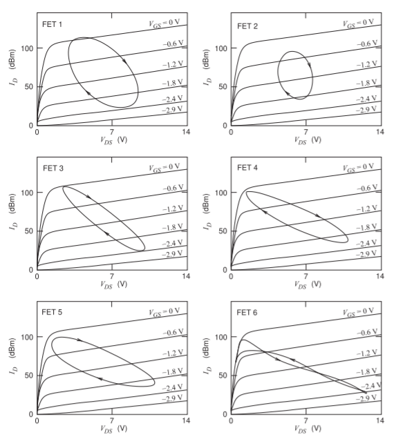
Figure \(\PageIndex{1}\): Dynamic loadlines of each FET in the TGA8220 MMIC distributed amplifier. After [4], copyright Microwaves & RF, used with permission.
cancel the transistor’s feedback capacitor and instead the input and output matching networks are adjusted to account for it.
The negative image amplifier design method achieves high bandwidth by synthesizing input and output matching networks beginning with each network comprising a negative capacitance in parallel with the input and output, respectively, parasitic capacitances of the transistor. Then resistive loads, chosen for maximum power transfer, are put in parallel with the negative capacitances. This circuit is simulated with the actual model of the transistor and this is followed by an optimization step to optimize the broadband gain and noise responses of the amplifier while simultaneously ensuring stability of the amplifier. In this process the effect of the feedback capacitance and the full complexity of the transistor are accounted for. The input and output matching networks are the negative image networks. The next step is to separately synthesize networks that provide the characteristics of the ideal input and output matching networks. This can only be done over a limited bandwidth but usually this is about half an octave. This process indicates the optimum characteristics of the input and output matching networks. The negative image networks can now be synthesized individually and once synthesized can be incorporated with the transistor model to obtain an overall circuit that can further be adjusted but perhaps only a few percent adjustment will be necessary.
The negative image method regularly achieves a half octave bandwidth. What is being done in the matching network design is using a topology that presents what looks like a negative capacitor and also the right impedance transformation (usually to \(50\) ohms). This is where invention comes into play. The impedance looking into the input (or output) of a transistor rotates with respect to frequency in the clockwise direction on a Smith chart. The complex conjugate impedance rotates in the counter-clockwise direction. The designer tries to develop a matching network that tracks the counter-rotating locus but with one capacitor and one inductor the impedance locus (with respect to frequency) looking into the matching network will rotate in the clockwise direction. The only simple circuit that will give you the right characteristics includes two or more transmission lines. The designer is using a topology that someone else discovered. It is not possible to synthesize the best network.
There are some limitations, both the input and output of the transistor will have some series inductance due to bondwires for discrete transistor parts and due to lengths of transmission line for on-chip transistors . The impedance of these inductances will be small compared to the parasitic capacitances and will really only matter if the input resistance of the transistor (in the case of the inductance at the input port) or the output resistance of the transistor (in the case of the inductance at the output port) is also small. Generally it is only necessary to compensate for the output inductance in the negative image model of the output network. and this is done by using use a negative inductance.
At this stage the amplifier design consists of input and output negative image matching networks which are quite simple and contain negative elements. The operation of the amplifier is optimized using these simple matching networks. The transistor is not unilateral so the input and output matching networks must be adjusted iteratively to get the optimum performance. The matching networks are so simple that manual tuning can be used in the circuit simulator.
With the simple matching networks designed, the challenge is now to realize the simple matching networks with real elements. L’s and C’s in a filter-like structure could possibly be used, but the result is rarely very good. The best results are obtained when transmission line structures are used. There is not a way to systematically synthesize these matching networks. The transmission line-based topologies that are used in the case study are inventions. There are very few other structures that work. The design problem is greatly simplified and design can focus on designing first the input matching network and then the output matching network without the transistor included.