
3.6: Differential Amplifiers
- Page ID
- 46041
A significant change in RF and microwave engineering has been the increasing importance of differential circuits such as the amplifier in Figure \(\PageIndex{2}\)(a). In part this is because they are conveniently implemented in silicon technology. It is also a result of the use of monolithic integration and the maturity of semiconductor technologies resulting in repeatable RF active components. Differential amplifiers are the preferred amplifier topology with RFICs. Since substrate noise is common to all nodes of a differential amplifier, there is little differential substrate noise signal. Also, differential circuits lend themselves to current-mode biasing which is preferred onchip. The defining characteristic of a differential amplifier is that there are paired signal paths that are differential. These amplifiers are also (but less commonly) called balanced amplifiers. When the RF signal on one side of the differential path is positive, the RF signal on the other side is negative.
3.6.1 Fully and Pseudo-Differential Amplifiers
Figure \(\PageIndex{2}\)(a) shows a fully differential amplifier (FDA) with resistive biasing in the drain legs. As well as providing biasing current, the resistors load the amplifier. The supply voltage of an RFIC can be quite low (a few volts or less), so choosing circuit topologies that provide for large voltage swings is important, particularly for a driver amplifier being the last
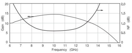
Figure \(\PageIndex{1}\): Final amplifier performance.
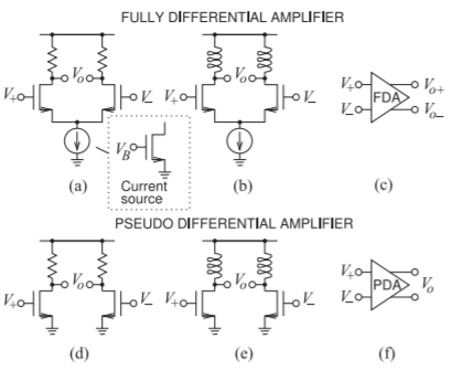
Figure \(\PageIndex{2}\): Differential amplifiers: (a) fully differential amplifier (FDA); (b) FDA with inductive biasing; (c) schematic representation; (d) pseudodifferential amplifier (PDA); (e) PDA with inductive biasing; and (f) schematic representation. The inset in (a) shows the implementation of current source as a single enhancement-mode MOSFET with a bias voltage, \(V_{B}\), at the gate.
amplifier stage in a transmitter RFIC that drives a following power amplifier. Differential topologies lead to an almost doubling of the output voltage swing compared to the output voltage swing of a single-ended amplifier. An FDA includes a common current source that can be implemented quite simply using a single FET, as shown in the inset in Figure \(\PageIndex{2}\)(a). Here the gate-source voltage is the bias voltage, \(V_{B}\), which, from Figure 2.5.2(b), establishes a nearly constant drain current as long as there is sufficient drain-source voltage across the current source transistor.
Common-Mode Rejection
One of the attributes that makes FDAs attractive is that they are relatively immune to substrate noise (noise in the substrate produced by other circuits). The signal applied to the inputs of a differential amplifier have differential-and common-mode components. Referring to the differential amplifier in Figure \(\PageIndex{2}\)(c), the differential-mode input signal is
\[\label{eq:1}V_{id}=V_{+}-V_{-} \]
and the common-mode input signal is
\[\label{eq:2}V_{ic}=\frac{1}{2}(V_{+}+V_{-}) \]
Similarly the differential- and common-mode output signals are
\[\label{eq:3}V_{od}=V_{o+}-V_{o-}\quad\text{and}\quad V_{oc}=\frac{1}{2}(V_{o+}+V_{o-}) \]
respectively. The differential-mode voltage gain is
\[\label{eq:4}A_{d}=\frac{V_{od}}{V_{id}} \]
and the common-mode gain is
\[\label{eq:5}A_{c}=\frac{V_{oc}}{V_{ic}} \]
For good noise immunity, the common-mode gain should be low and the differential-mode gain should be high. The figure of merit that describes this is the common-mode rejection ratio (CMRR):
\[\label{eq:6}\text{CMRR}=\frac{A_{d}}{A_{c}} \]
and the larger this is, the better. CMRR is usually expressed in decibels, and since CMRR is a voltage gain ratio, CMRR in decibels is \(20 \log(A_{d}/A_{c})\). The current source at the source of the differential pair of the FDA has a large effect on the CMRR by suppressing the output common-mode voltage. Then the current source results in a large CMRR. Without the current source, the CMRR of the FDA of Figure \(\PageIndex{2}\)(a) would be one.
Output Voltage Swing
Single-ended amplifiers were discussed in Section 2.5.1, where it was shown that inductive biasing enables higher output voltage swings than possible with resistive biasing. A similar enhancement can be obtained with a differential amplifier. The inductively biased FDA of Figure \(\PageIndex{2}\)(b) has a higher voltage swing than the resistively biased FDA of Figure \(\PageIndex{2}\)(a). More can be achieved, however. The current sources at the common source point of the FDAs in Figure \(\PageIndex{2}\)(a and b) limit the voltage swing, as there is a minimum drain-source voltage drop required across the current source for it to maintain constant current. When larger output voltage swings are required, the current source is eliminated and the resulting amplifier is called a pseudo-differential amplifier (PDA), as shown in Figure \(\PageIndex{2}\)(d). Again, inductive biasing (see Figure \(\PageIndex{2}\)(e)) almost doubles the possible voltage swing. The performance cost with the PDA circuit is that the CMRR is one.
The output voltage waveforms for single-ended and differential amplifiers with and without inductive biasing are shown in Figure \(\PageIndex{3}\). The inductively biased PDA, shown in Figure \(\PageIndex{3}\)(d), has an output voltage swing that is about \(4\) times the voltage swing (or about \(16\) times the power into the same load) of the single-ended resistively biased Class A amplifier in Figure \(\PageIndex{3}\)(a) (the actual factors depend on the supply voltage and \(V_{DS\text{ ,min}}\)).
Example \(\PageIndex{1}\): Calculation of Common-Mode Rejection Ratio
Determine the CMRR of the FET differential amplifier shown in Figure \(\PageIndex{4}\)(a).
Solution
The strategy for solving this problem is to develop the common-mode and differential-mode equivalent circuits and solve for the gain of each. The first step is to develop the small-signal model shown in Figure \(\PageIndex{4}\)(b). The differential input signal is \(V_{id}\) and the common input signal is \(V_{ic}\) so that the input voltage signals are
\[\label{eq:7}V_{i+}=\frac{1}{2}(V_{id}+V_{ic})\quad\text{and}\quad V_{i-}=-\frac{1}{2}(V_{id}+V_{ic}) \]
The expressions are similar for the output differential- and common-mode signals \(V_{od}\) and \(V_{oc}\). This leads to the small signal differential-mode model of Figure \(\PageIndex{4}\)(c) and the small signal common-mode model of Figure \(\PageIndex{4}\)(d). From Figure \(\PageIndex{4}\)(c), the output differential signal is
\[\label{eq:8}V_{od}=\frac{V_{id}}{2}[-g_{m}(r_{d}//R_{L})]-\frac{-V_{id}}{2}[-g_{m}(r_{d}//R_{L})]=\frac{-V_{id}g_{m}r_{d}R_{L}}{r_{d}+R_{L}} \]
so the differential gain is
\[\label{eq:9}A_{d}=\frac{V_{od}}{V_{id}}=\frac{-g_{m}r_{d}R_{L}}{r_{d}+R_{L}} \]
If, as usual, \(r_{d} ≫ R_{L}\), this becomes
\[\label{eq:10}A_{d}=-g_{m}R_{L} \]
Focusing on the small signal common-mode model of Figure \(\PageIndex{4}\)(d) yields the output common-mode signal. The two halves of the circuit are now identical. The sum of the currents at \(\mathsf{X}\) is zero, so
\[\label{eq:11}\frac{V_{S}}{2R_{S}}+\frac{V_{S}-V_{oc}}{r_{d}}-g_{m}(V_{ic}-V_{S})=0 \]
and the sum of the currents at the output terminal is zero, so
\[\label{eq:12}\frac{V_{oc}}{R_{L}}+\frac{V_{oc}-V_{S}}{r_{d}}+g_{m}(V_{ic}-V_{S})=0 \]
Eliminating \(V_{S}\) from these equations leads to
\[\label{eq:13}V_{oc}=\frac{-g_{m}r_{d}R_{L}V_{ic}}{(1+g_{m}r_{d})2R_{S}+r_{d}+R_{L}} \]
so the common-mode gain is
\[\label{eq:14}A_{c}=\frac{V_{oc}}{V_{ic}}=\frac{-g_{m}r_{d}R_{L}}{(1+g_{m}r_{d})2R_{S}+r_{d}+R_{L}} \]
If, as usual, \(r_{d} ≫ R_{L}\), this becomes
\[\label{eq:15}A_{c}=\frac{-g_{m}R_{L}}{1+2g_{m}R_{S}} \]
The CMRR (when \(r_{d} ≫ R_{L}\)) is
\[\label{eq:16}\text{CMRR}=\frac{A_{d}}{A_{c}}=\frac{-g_{m}R_{L}(1+2g_{m}R_{S})}{-g_{m}R_{L}}=(1+2g_{m}R_{S}) \]
So the CMRR depends on the value of \(R_{S}\). If there is no resistor at the common-mode source point, as in a pseudo-differential amplifier, \(R_{S} = 0\) and so
\[\label{eq:17}\text{CMRR}|_{R_{S}=0}=1 \]
If there is an ideal current source at the source node, then \(R_{S}\) is effectively infinite, and so
\[\label{eq:18}\text{CMRR}|_{\text{current source}}=\infty \]
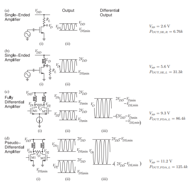
Figure \(\PageIndex{3}\): Class A MOSFET amplifiers with output voltage waveforms: (a) single-ended amplifier with resistive biasing; (b) single-ended amplifier with inductive biasing; (c) fully differential amplifier with inductive biasing; and (d) pseudo-differential amplifier. Schematic is shown in (i), drain voltage waveforms in (ii), and differential output in (iii). The final column gives the output voltage swing, \(V_{pp}\), and the output power with \(V_{DD} = 3\text{ V},\) \(V_{D,\text{ min}} = 0.95\text{ V}\), \(V_{DS\text{ ,min}} = 0.4\text{ V}\), and \(k\) is a proportionality constant dependent on loading that is assumed to be the same for all amplifiers. \(V_{D\text{ ,min}}\) is the minimum voltage at the drain of the current-source MOSFET. The resistively biased single-ended amplifier has an output power proportional to \(6.76\) while the inductively biased PDA in (d) has an output power proportional to \(125.4,\) \(18.6\) times larger.
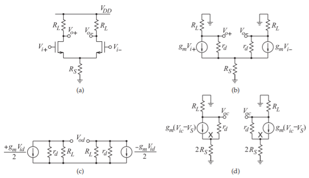
Figure \(\PageIndex{4}\): Differential amplifier: (a) schematic; (b) small signal model; (c) small signal model for calculating differential gain; and (d) small signal model for calculating common-mode gain.
3.6.2 Even, Common, Odd, and Differential Modes
The difference between even- and common-mode current, voltages and impedances comes down to bookkeeping as to how the voltages and currents are defined. The same is true for the odd- and differential-mode quantities. The reason both sets of definitions are used is because the even-/odd-mode set usage is preferred with transmission line structures and the common- /differential-mode set usage is preferred with complementary transistor circuits such as differential amplifiers.
Consider the amplifier shown in Figure \(\PageIndex{5}\)(a) with two inputs and two outputs. The input and output voltages in the various modes are defined as follows:
Odd-mode input voltage, \(V_{io}\), and current, \(I_{io}\) (with the second subscript indicating the mode):
\[\label{eq:19}V_{io}=\frac{1}{2}(V_{i1}-V_{i2})\quad\text{and}\quad I_{io}=\frac{1}{2}(I_{i1}-I_{i2}) \]
Differential-mode input voltage, \(V_{id}\), and current, \(I_{id}\):
\[\label{eq:20}V_{id}=(V_{i1}-V_{i2})\quad\text{and}\quad I_{id}=\frac{1}{2}(I_{i1}-I_{i2}) \]
Even-mode input voltage, \(V_{ie}\), and current, \(I_{ie}\):
\[\label{eq:21}V_{ie}=\frac{1}{2}(V_{i1}+V_{i2})\quad\text{and}\quad I_{ie}=\frac{1}{2}(I_{i1}+I_{i2}) \]
Common-mode input voltage, \(V_{ic}\), and current, \(I_{ic}\):
\[\label{eq:22}V_{ic}=\frac{1}{2}(V_{i1}+V_{i2})\quad\text{and}\quad I_{ic}=(I_{i1}+I_{i2}) \]
Reversing the definitions, if there is no common-/even-mode input signal:
\[\label{eq:23}\begin{array}{lll}{V_{i1}=\frac{1}{2}V_{id}=V_{io}}&{}&{V_{i2}=-\frac{1}{2}V_{id}=-V_{io}}\\{I_{i1}=I_{id}=I_{io}}&{\text{and}}&{I_{i2}=-I_{id}=-I_{io}}\end{array} \]
The output voltages and currents are similarly related. Figures \(\PageIndex{5}\)(b)–\(\PageIndex{5}\)(e) show the conceptual even-, odd-, common- and differential- mode load definitions. In switching between definitions, say between the differential load and the odd-mode load, the actual resistor in the circuit does not change.
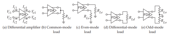
Figure \(\PageIndex{5}\): Differential amplifiers and various loads. \(R_{Lc}\) is the common-mode load, \(R_{Le}\) is the even-mode load, \(R_{Ld}\) is the differential-mode load (often the term differential load is used), and \(R_{Lo}\) is the odd-mode load.
Example \(\PageIndex{2}\): Odd-Mode Load
The differential amplifier to the right has a differential load of \(100\:\Omega\). What is the odd-mode load?
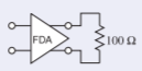
Figure \(\PageIndex{6}\)
Solution
The circuit is put into the odd-mode form to the right. Comparing this to the load definitions shown in Figure \(\PageIndex{4}\)(d), it is seen that the odd-mode load impedance is \(50\:\Omega\).
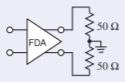
Figure \(\PageIndex{7}\)
3.6.3 Asymmetrical Loading
It is simple enough to determine the common and differential loads, or similarly the even- and odd-mode loads, when the loading of a differential amplifier is symmetrical. However when loading is asymmetrical, details of the driving differential amplifier are required to determine the coupling between the common and differential signals. The situation is similar to that with a terminated coupled line, see Section 5.7 of [7], where the Thevenin equivalent impedance of the source is required to determine the circuit conditions.
With an asymmetrical load there will be coupling between the even and odd modes. So even if the driving differential amplifier produces a differential output current and has zero common mode current, there could still be a common mode voltage. This is important as transistors operate as voltage-controlled current sources and many differential amplifiers are actually transconductance amplifiers as this gives the widest bandwidths, simplest biasing, and good noise immunity. The output stage of a differential amplifier appears as differential voltage-controlled current sources and in an RFIC adaptive mechanisms usually ensure that there is no common-mode current. But the differential current can induce a common-mode voltage which drives following stages. The design strategy then is to ensure that a differential amplifier produces minimal common-mode current, and loading is symmetrical. The following examples are illustrative.
Example \(\PageIndex{3}\): Asymmetrical Loading of a Differential Amplifier
A differential amplifier has two output terminals with one of the outputs connected to a \(60\:\Omega\) resistor and the other terminated in a \(100\:\Omega\) resistor, as shown in Figure \(\PageIndex{8}\)(a). The output stage of the differential amplifier is modeled as two controlled current sources \(I_{o1}\) and \(I_{o2}\) and the output common-mode current is zero.
- What is the common-mode voltage, \(V_{c}\), at the load if the differential current is \(1\text{ mA}\)? This problem will first be solved using the general loads shown in Figure \(\PageIndex{8}\)(b). The voltages at the load are \(V_{o1} = V_{c}+ \frac{1}{2}V_{d}\) and \(V_{o2} = V_{c}− \frac{1}{2} V_{d}\) where \(V_{d}\) is the differential output voltage. The output currents are \(I_{o1} = \frac{1}{2}I_{c} + I_{d} = I_{d}\) and \(I_{o2} = \frac{1}{2}I_{c} − I_{d} = −I_{d}\). Then
\[\begin{align}\label{eq:24}V_{o1}&=V_{c}+\frac{1}{2}V_{d}=I_{o1}R_{1}=+I_{d}R_{1}\\ \label{eq:25}V_{o2}&=V_{c}-\frac{1}{2}V_{d}=I_{o2}R_{2}=-I_{d}R_{2}\end{align} \]
combining these
\[\label{eq:26}2V_{c}=I_{d}(R_{1}-R_{2})\quad\text{and so}\quad V_{c}=\frac{1}{2}(1\text{ mA}(60\:\Omega - 100\:\Omega)=40\text{ mV} \]
The common mode voltage at the output is \(40\text{ mV}\). - What is the differential-mode load resistance, \(R_{Ld}\)?
The differential-mode load \(R_{Ld}\) is defined in Figure \(\PageIndex{8}\)(d) so that \(R_{Ld} = V_{d}/I_{d}\).
Taking the difference of Equations \(\eqref{eq:24}\) and \(\eqref{eq:25}\) and eliminating \(V_{c}\) leads to
\[\label{eq:27}V_{d}=I_{d}(R_{1}+R_{2})+\frac{1}{2}I_{c}(R_{1}-R_{2})\quad\text{and}\quad R_{Ld}=\frac{V_{d}}{I_{d}}=(R_{1}+R_{2})=160\:\Omega \]
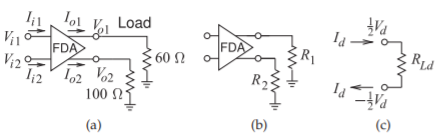
Figure \(\PageIndex{8}\): Terminated differential amplifier: (a) asymmetrical loading; (b) general representation of loading; and (c) definition of voltages and currents for the differential-mode load impedance \(R_{Ld}\).
Example \(\PageIndex{4}\): Differential- and Odd-Mode Loads
A differential amplifier is shown in Figure \(\PageIndex{9}\)(a) with resistive loading. Find the differential- and odd-mode load resistances if the common-mode current is zero.
Solution
Nodal analysis yields the circuit equations
\[\label{eq:28}I_{1}=\frac{V_{1}}{10}+\frac{V_{1}-V_{2}}{5}\quad\text{and}\quad I_{2}=\frac{V_{2}}{20}+\frac{V_{2}-V_{1}}{5} \]
That is
\[\label{eq:29}V_{1}=(50I_{1}+40I_{2})/7\quad\text{and}\quad V_{2}=(40I_{1}+60I_{2})/7 \]
- What is the differential-mode load resistance \(R_{Ld}\)?
The differential-mode current \(I_{d} = \frac{1}{2}(I_{1} − I_{2})\), so, since the common-mode current is zero, set \(I_{1} = I_{d}\) and \(I_{2} = −I_{d}\) and Equation \(\eqref{eq:29}\) becomes
\[\label{eq:30}V_{1}=\frac{10}{7}I_{d}\quad\text{and}\quad V_{2}=-\frac{20}{7}I_{d} \]
The differential-mode voltage is
\[\label{eq:31}V_{d}=(V_{1}-V_{2})=\frac{30}{7}I_{d} \]
Thus
\[\label{eq:32}R_{Ld}=\frac{V_{d}}{I_{d}}=\frac{30}{7}=4.286\:\Omega \] - What is the odd-mode load resistance \(R_{Lo}\)?
The odd-mode current \(I_{o} = \frac{1}{2} (I_{1} − I_{2})\), so set \(I_{1} = I_{o}\) and \(I_{2} = −I_{o}\) since the common-mode, and hence even-mode, current is zero and Equation \(\eqref{eq:29}\) becomes
\[\label{eq:33}V_{1}=\frac{10}{7}I_{o}\quad\text{and}\quad V_{2}=\frac{-20}{7}I_{o} \]
The odd-mode voltage is
\[\label{eq:34}V_{o}=\frac{1}{2}(V_{1}-V_{2})=\frac{30}{14}I_{o} \]
Thus
\[\label{eq:35}R_{Lo}=\frac{V_{o}}{I_{o}}=\frac{30}{14}=2.143\:\Omega \]
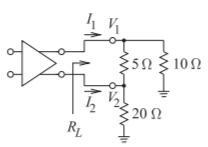
Figure \(\PageIndex{9}\): A differential amplifier with asymmetrical terminating resistors.
3.6.4 Hybrids and Differential Amplifiers
RFICs use both fully differential and pseudo-differential signal paths. If signal swing is not a concern, a fully-differential signal path is preferred, particularly because of its immunity to noise and its bias stability. The additional transistors involved in realizing a differential circuit (e.g., the current source) reduce the available voltage swing, and hence the powerhandling capability. Pseudo-differential signaling uses, in effect, two parallel paths, each referred to ground, but of opposite polarity. The signal on one of the parallel paths is the mirror image of the signal on the other (i.e., the signal is not truly differential, which would imply that it was floating or independent of ground). Each of the parallel paths is unbalanced, but together their RF signal appears to be balanced, or pseudo-balanced. Another consideration is that in working with RFICs it is necessary to interface (unbalanced) microstrip circuits with the inputs and outputs of RFICs. The functionality here requires that signals be split and combined, and converted between balanced and unbalanced signals.
An FDA is shown in Figure \(\PageIndex{10}\)(a). Both the input voltage, \(V_{i} = V_{+} − V_{−}\), and the output voltage, \(V_{o}\), are differential. Figure \(\PageIndex{10}\)(b and c) show a transformer being used to convert the differential output of the amplifier to an unbalanced signal that, for example, can be connected to a microstrip circuit. The output of many RFICs is pseudo-differential, as this signaling provides large voltage swings. A pseudo-differential amplifier is shown in Figure \(\PageIndex{10}\)(d), but before dealing with manipulation of the signal path, first consider the hybrid on its own.
Figure \(\PageIndex{11}\)(a) shows how two pseudo-balanced signals can be combined to yield a single balanced signal. This \(180^{\circ}\) hybrid function is realized by a center-tapped transformer. The signal at Terminal 2 is referenced to ground, and these two terminals are Port 2. The image component of the pseudo-differential signal is applied to Port 3, comprising Terminal 3 and ground. The balanced signal at Port 1 can be directly connected to a microstrip line that is, of course, unbalanced. Most implementations of hybrids at microwave frequencies have ports that are referenced to ground. This is emphasized in Figure \(\PageIndex{11}\)(b), making it easier to see how a \(180^{\circ}\) hybrid can be used to combine a pseudo-differential signal, as shown in Figure \(\PageIndex{11}\)(c). This pseudo-differential-to-unbalanced interface is shown in Figure \(\PageIndex{10}\)(e– g) with a pseudo-differential amplifier.
Hybrids can be used at the input and output terminals of an RFIC pseudo-differential amplifier so that an unbalanced source can efficiently drive the RFIC and then the output of the RFIC can be converted to an unbalanced port to interface with unbalanced circuitry, such as filters and transmission lines. In the RFIC-based system in Figure \(\PageIndex{12}\), a \(180^{\circ}\) hybrid is first used as a splitter and then at the output as a combiner.
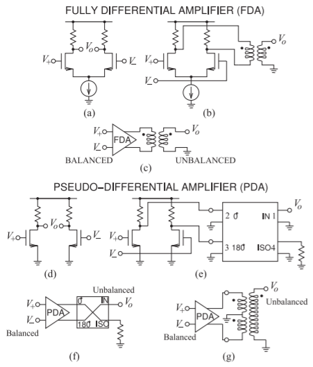
Figure \(\PageIndex{10}\): Configurations providing an unbalanced output from a differential amplifier: (a) FDA; (b) FDA configured with a balun; (c) schematic; (d) PDA; (e) PDA configured with a \(180^{\circ}\) hybrid to provide an unbalanced output; (f) schematic; and (g) PDA with a transformer connection yielding an unbalanced output.
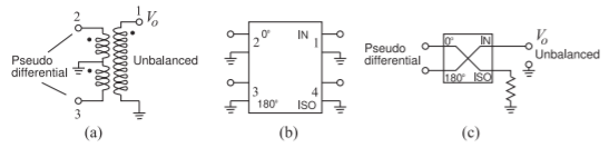
Figure \(\PageIndex{11}\): Equivalent representations of a \(180^{\circ}\) hybrid connected to provide an interface between a pseudo-differential balanced port and an unbalanced port: (a) a transformer configured as a \(180^{\circ}\) hybrid with pseudo-unbalanced-to-balanced configuration; (b) hybrid showing two terminal representation of ports; and (c) schematic of a \(180^{\circ}\) hybrid with the isolation port terminated in a matched load.
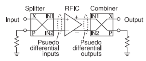
Figure \(\PageIndex{12}\): An RFIC with differential inputs and outputs driven by a \(180^{\circ}\) hybrid used as a splitter and followed by another \(180^{\circ}\) hybrid used as a combiner.