
1.3: Transistor Technology
- Page ID
- 46017

Transistors are semiconductor devices with three (and sometimes more) terminals. The third terminal enables output current to be controlled by a relatively small and low-power input signal. In amplifiers, transistors are used to achieve current gain, voltage gain, or power gain. Most often power gain is the objective in RF and microwave design. Most transistors are fabricated using silicon (Si) or compound semiconductors such as galliumarsenide (GaAs), indium phosphide (InP), or gallium-nitride (GaN). The overwhelming trend is to use silicon technology because of the much higher integration density that is possible, with compound semiconductor technology used only when it provides a unique advantage such as high power, superior noise performance, or high efficiency. Germanium is used as a dopant in silicon and then silicon is referred to as silicon germanium but usually germanium is in a very small proportion to silicon so SiGe as described here is silicon with a dopant. With comparable concentrations of silicon and germanium SiGe is a compound semiconductor and this is used as a compound semiconductor at times.
There are three fundamental types of microwave transistors [5, 6]: bipolar junction transistors, (BJTs); junction field effect transistors, (JFETs); and insulated gate FETs, (IGFETs), with the metal-oxide-semiconductor FETs, (MOSFETs), being the most common type of IGFET. The schematics and terminal definitions of the three fundamental types of transistors are shown in Figure \(\PageIndex{1}\). The three fundamental types of transistors are considered in the following subsections.
1.3.1 BJT and HBT Fundamentals
A bipolar transistor has three semiconductor regions called the collector (C), base (B), and emitter (E), as shown in the BJT cross section of Figure \(\PageIndex{2}\)(a). An npn BJT has n-type semiconductor at the emitter and collector, and p-type semiconductor forms the base. In this transistor, the positive sense of current flow is from the collector through the base to the emitter (see Figure \(\PageIndex{2}\)(a)) and the dominant carriers in the p-type base region are electrons, and so this is called a minority carrier device. The collector current is dependent on the number of carriers injected into the base region from the base terminal. In a pnp BJT the collector, base, and emitter are p-type, n-type, and p-type, respectively, and the majority carriers in the base are holes. Current flow is then from the emitter through the base to the collector. If the base region is thin and the emitter is doped at a higher concentration than the base, then the collector current, \(I_{C}\), is much greater than \(I_{B}\), with \(I_{C} = \beta_{F}I_{B}\), where \(\beta_{F}\) is called the forward current gain and commonly has a value of several hundred. The key to high performance is a thin base region.
When realized in silicon, a bipolar transistor is called a bipolar junction transistor, (BJT); and in compound semiconductor technology it is a heterostructure bipolar transistor, (HBT). In a silicon germanium (SiGe) BJT transistor, germanium is normally used to increase the hole and electron mobility and the device is not regarded as a compound semiconductor transistor.
The fundamental operation of a BJT transistor was described by Gummel and Poon [7] using equations that are now implemented in circuit simulators and known as the Gummel–Poon model. The circuit schematic of the Gummel–Poon model is shown in Figure \(\PageIndex{2}\)(c). It is the basis for more
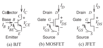
Figure \(\PageIndex{1}\): Transistor schematics: (a) pnp bipolar transistor with B for the base terminal, C for the collector terminal, and E for the emitter terminal; (b) n-type MOSFET (nMOS); and (c) n-type JFET (nJFET) with G for the gate terminal, D for the drain terminal, and S for the source terminal. The schematic symbol for a BJT is used for HBTs; and the schematic symbol for a JFET is used for MESFETs, HEMTS, and pHEMTs.
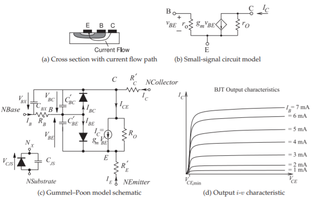
Figure \(\PageIndex{2}\): BJT details.
sophisticated BJT and HBT models that capture parasitic and other second-order effects. Both hole and electron charge carriers are involved in current conduction, hence the term bipolar. The Gummel–Poon model is described in Section 1.A.3 and the fundamental operation is described by Equations (1.A.52)–(1.A.62). Summarizing, the base-emitter current is
\[\label{eq:1}I_{BE}=I_{BF}/\beta_{F}+I_{LE} \]
and the base-collector current is
\[\label{eq:2}I_{BC}=I_{BR}/\beta_{R}+I_{LC} \]
where \(\beta_{R}\) is the reverse current gain. The collector-emitter current is
\[\label{eq:3}I_{CE}=I_{BF}-I_{BR}/K_{QB} \]
The forward diffusion current is
\[\label{eq:4}I_{BF}=I_{S}\left(\text{e}^{V_{BE}/(N_{F}V_{TH})}-1\right) \]
the nonideal base-emitter current is
\[\label{eq:5}I_{LE}=I_{SE}\left(\text{e}^{V_{BE}/(N_{E}V_{TH})}-1\right) \]
the reverse diffusion current is
\[\label{eq:6}I_{BR}=I_{S}\left(\text{e}^{V_{BC}/(N_{R}V_{TH})}-1\right) \]
the nonideal base-collector current is
\[\label{eq:7}I_{LC}=I_{SC}\left(\text{e}^{V_{BC}/(N_{C}V_{TH})}-1\right) \]
and the base charge factor is
\[\label{eq:8}K_{QB}=\frac{1}{2}\left[1-\frac{V_{BC}}{V_{AF}}-\frac{V_{BE}}{V_{AB}}\right]^{-1}\left[1+\sqrt{1+4\left(\frac{I_{BF}}{I_{KF}}+\frac{I_{BR}}{I_{KR}}\right)}\right] \]
Thus the conductive current flowing into the base is
\[\label{eq:9} I_{B}=I_{BE}+I_{BC} \]
the conductive current flowing into the collector is
\[\label{eq:10}I_{C}=I_{CE}-I_{BC} \]
and the conductive current flowing into the emitter is
\[\label{eq:11}I_{E}=I_{BE}+I_{CE} \]
The forward current gain, \(\beta_{F}\), is much greater than the reverse current gain, \(\beta_{R}\), and the nonideal base-emitter and base-collector currents are small. Equations \(\eqref{eq:1}\)-\(\eqref{eq:11}\) can then be reduced so that the base current is approximately
\[\label{eq:12}I_{B}=\frac{I_{S}}{\beta_{F}}\left(\text{e}^{V_{BE}/(N_{F}V_{TH})}-1\right) \]
the conductive current flowing into the collector is
\[\label{eq:13}I_{C}=\beta_{F}I_{B} \]
and the conductive current flowing into the emitter is
\[\label{eq:14}I_{E}=I_{B}+I_{C} \]
From Equations \(\eqref{eq:12}\) and \(\eqref{eq:13}\) it is seen that the fundamental operation of a BJT is as a voltage-controlled current source. This leads to the small-signal circuit model of a BJT, biased in its fundamental mode of operation, shown in Figure \(\PageIndex{2}\)(b).
The schematic symbols used for BJTs are shown in Table \(\PageIndex{1}\) with the arrow pointing to the n-type semiconductor. The BJT symbol is also the symbol for a HBT.
1.3.2 MOSFET Fundamentals
There are several types of FETs, with the MOSFET being the most common. With all FETs there is a channel between two terminals, the source and drain, and an applied field produced by a voltage at a third terminal, the gate, controls the cross section of the channel and the number of carriers in the channel. Hence the gate voltage controls the current flow between the drain and the source. With some FETs, the channel does not exist until a gate field is applied and pulls carriers from the bulk into the channel, and this
| Transistor | IEEE Symbol | Commonly used symbol |
|---|---|---|
| BJT, pnp |  |
 |
| BJT, npn |  |
 |
Table \(\PageIndex{1}\): IEEE standard schematic symbols for bipolar junction transistors (BJTs and HBTs) [8] and commonly used symbols in layouts [9]. The letters indicate terminals: \(\mathsf{B}\) (base), \(\mathsf{C}\) (collector), \(\mathsf{E}\) (emitter). These symbols are used for silicon BJTs and compound semiconductor HBTs.
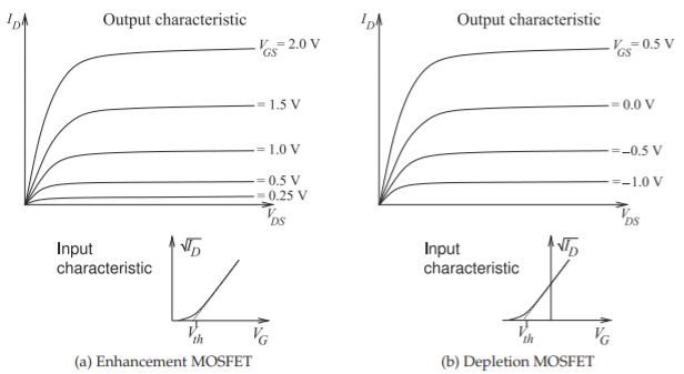
Figure \(\PageIndex{3}\): Current-voltage characteristics of depletion- and enhancement-mode MOSFETs.
is called an enhancement-mode FET. The input and output characteristics of the enhancement-mode FET are shown in Figure \(\PageIndex{3}\)(a). With some MOSFETs with a particular doping profile, carriers are in the channel even without an applied field and a gate voltage either enhances the cross section of the channel or closes it off. Most often the gate voltage is used to reduce current conduction, and this type of FET is called a depletion-mode FET. The input and output characteristics of the depletion-mode FET are shown in Figure \(\PageIndex{3}\)(b). The enhancement-mode MOSFET is much more common than the depletion-mode.
The enhancement MOSFET is a relatively simple device to fabricate and is the smallest of the semiconductor transistors. It is the preferred technology for high-density integration. The three-dimensional view and cross sections of a MOSFET are shown in Figure \(\PageIndex{4}\)(a–c). The cross-section of an nMOS transistor is shown in Figure \(\PageIndex{4}\)(b) where there is a p-type substrate and an n-type channel is created when there is sufficient voltage at the gate. As well as the source and drain connection, there is a fourth terminal call the body connection denoted as \(\mathsf{U}\) in Figure \(\PageIndex{4}\)(b) but \(\mathsf{B}\) is also used and this can be confused with the base of a BJT transistor. The body is typically
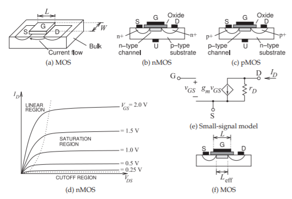
Figure \(\PageIndex{4}\): MOSFET details: (a) three-dimensional view of a MOSFET; (b) cross section of an nMOS transistor with metal or polysilicon contacts indicated by the black blocks; (c)the corresponding cross section of a pMOS transistor; (d) current-voltage characteristics of an enhancement-mode MOSFET; (e) circuit model of fundamental operation; and (f) cross section showing the effective gate length, \(L_{\text{EFF}}\). The linear region is sometimes (but less often) called the triode region because of similarity to the characteristics of the triode vacuum tube device. Similarly the saturation region is sometimes called the pentode region.
connected to the most negative voltage in the circuit so that the substrate-to-channel interface is a reverse-biased diode. A similar situation occurs with the pMOS transistor with the cross-section of Figure \(\PageIndex{4}\)(c). Now there is a p-type channel and an n-type substrate so that the body (\(\mathsf{U}\)) must typically be connected to the most positive voltage in the circuit to ensure a reverse-biased junction between the substrate and the channel.
A MOSFET has metal or polysilicon (a reasonable conductor [5, 6, 10]) connections at the drain (\(\mathsf{D}\)), source (\(\mathsf{S}\)) and gate (\(\mathsf{G}\)). The MOSFET is nearly always silicon, but possibly (GaN!MOSFET [11, 12]. The source and drain connections are highly doped (n+ for nMOS and p+ for pMOS) semiconductor regions providing a good ohmic contact rather than forming a Schottky barrier.\(^{1}\) The gate is not in direct contact with the semiconductor, but separated by a thin layer of oxide. With no voltage applied at the gate, there are no carriers below the gate oxide that can conduct current between the source and drain. A gate voltage is necessary to draw carriers to the channel region, forming a conducting channel. That is, a voltage applied to the gate creates an electric field that induces electrons (the n carriers for an nMOSFET) to form a conducting channel immediately under the oxide.\(^{2}\) This process is called inversion. The length of the channel is denoted \(L_{\text{eff}}\) (the effective gate length), which is less than the actual gate length \(L\) as the highly doped source and drain regions must extend under the gate to ensure good contact to the induced channel. This is indicated in Figure \(\PageIndex{4}\)(e). The number of carriers in the channel is controlled by the gate voltage. A higher frequency of operation is obtained by reducing \(L_{\text{eff}}\).
Three distinct regions of operation, identified in Figure \(\PageIndex{4}\)(d), are recognized for a MOSFET. In the linear region the drain-source current, \(I_{DS}\), continues to increase as the drain-source voltage, \(V_{DS}\), increases. \(I_{DS}\) depends on both the drain-source and gate-source voltage, \(V_{DS}\) and \(V_{GS}\), so the linear region is sometimes exploited in mixers. In the saturation region, \(I_{DS}\) is almost independent of \(V_{DS}\) and almost solely controlled by \(V_{GS}\). MOSFET amplifiers operate in the saturation region. The cutoff region is when there is negligible drain current, and a FET is particularly effective at shutting off conduction and so makes a good voltage-controlled switch.
In initial design the mode of fundamental operation must be intuitively understood and simple models and equations are needed. In contrast, a circuit simulator requires a detailed model capturing subtle physical effects. A model of a MOSFET that can be used in a circuit simulator is presented in Section 1.A.1. The model presented is known as the Level 3 MOSFET model and captures the fundamental operation of MOSFETs as well as capacitive parasitic effects. Models are developed using physical insight into semiconductor operation. All semiconductor device models, not just MOSFETs, require extensive fitting to measured data and have limited accuracy. Consequently the design, fabrication, and test cycle are critically important to realizing transistor circuits.
In the saturation region (see Figure \(\PageIndex{4}\)(d)) the fundamental operation of a MOSFET is described by Equation (1.A.27), which is repeated here:
\[\label{eq:15}I_{DS}=\frac{W_{\text{eff}}}{L_{\text{eff}}}\mu_{\text{eff}}C_{ox}\left[(V_{GS}-V_{th})-1+\frac{F_{B}}{2}V_{d\text{sat}}\right]V_{d\text{sat}} \]
Here \(C_{ox}\) is the capacitance of the gate oxide, \(W_{\text{eff}}\) is the effective gate width, which is the gate width \(W\) modified by fringing and related effects, \(V_{th}\) is the threshold voltage, and \(\mu_{\text{eff}}\) is the effective mobility\(^{3}\) of the carriers in the channel (electrons for an nMOSFET and holes for a pMOSFET). \(V_{d\text{sat}}\) is the drain saturation voltage and is the drain source voltage at which the device enters the saturation region from the linear region. \(F_{B}\) is due to the charge in the bulk semiconductor (below the channel) on which the gate-induced electric field terminates. \(L_{\text{eff}}\) is the effective gate length and this is modulated by the drain-source voltage so that [5, 6, 10]
\[\label{eq:16}L_{\text{eff}}=\frac{L}{1+\lambda V_{DS}} \]
Accounting for channel length modulation, described by Equation \(\eqref{eq:16}\), and simplifying [5, 6, 10], Equation \(\eqref{eq:15}\) becomes
\[\label{eq:17}I_{DS}=\frac{W}{L}\frac{\mu_{\text{eff}}C_{ox}}{2}(V_{GS}-V_{th})^{2}(1+\lambda V_{DS}) \]
This equation embodies the fundamental operation needed in developing initial designs. The key is that the MOSFET can be modeled (at least in the saturation region) as a voltage-controlled current source as shown in the model of Figure \(\PageIndex{4}\)(e). The transconductance, \(g_{m}\) (in saturation), is obtained by differentiating Equation \(\eqref{eq:17}\) so that (ignoring channel length modulation)
\[\label{eq:18}g_{m}=\frac{\partial I_{DS}}{\partial V_{GS}}=\frac{W}{L}\mu_{\text{eff}}C_{ox}(V_{GS}-V_{th}) \]
This can also be written as
\[\label{eq:19}g_{m}=\sqrt{\frac{W}{L}2\mu_{\text{eff}}C_{ox}I_{DS}} \]
Generally the gate length \(L\) is fixed at the minimum supported by a particular process, as this provides the highest frequency of operation. However, both \(L\) and \(W\) can be selected to control the current, \(I_{DS}\). For example, if \(V_{GS}\) is fixed, then the MOSFET acts as a current source, with the value of the current adjusted in design by setting \(L\) and \(W\) provided that there is sufficient \(V_{DS}\).
The current-voltage characteristics shown in Figure \(\PageIndex{4}\)(d) are those of an enhancement-mode MOSFET, which requires the simplest processing. Applying a gate-source voltage enhances the channel and increases \(I_{DS}\). With additional processing [5, 6, 10, 13] a depletion-mode MOSFET can be fabricated so that the channel exists even without an applied gate voltage. The same equations are used to describe operation with the threshold voltage changed. \(I_{DS}\) increases as the gate-source voltage increases, and it reduces as the gate-voltage becomes negative. The contrast between enhancement-mode and depletion-mode MOSFETs is illustrated in Figure \(\PageIndex{3}\).
The voltage of the bulk semiconductor affects the operation of a MOSFET and is a fourth terminal controlling drain-source conduction, but has a much smaller effect than the gate does. Most often the bulk is connected electrically to the most negative voltage in a circuit for an nMOSFET and to the most positive voltage for a pMOSFET. The standard schematic symbols of MOSFETs are shown in Table \(\PageIndex{2}\).
1.3.3 MESFET, HEMT, and JFET Fundamentals
The MESFETand HEMT are types of JFETs fabricated using compound semiconductors, with JFET most commonly referring to silicon devices only. The cross section of a JFET is shown in Figure \(\PageIndex{5}\)(a), where the depth (cross section) of the conducting channel is varied by the thickness of the depletion region of a reverse-biased junction. With the silicon JFET, the voltage applied to the gate terminal changes the amount of reverse bias and hence the depletion region thickness. Increased reverse bias reduces the cross section of the current-carrying channel. Thus a JFET looks like a variable conductance. The controlling field of the FET is created at the reverse-biased pn junction at
| Transistor | IEEE Symbol | Commonly used symbol (3 terminal) | Commonly used symbol (4 terminal) |
|---|---|---|---|
| FET, nMOS, depletion |  |
 |
 |
| FET, pMOS, depletion |  |
 |
 |
| FET, nMOS, enhancement |  |
 |
 |
| FET, pMOS, enhancement |  |
 |
 |
Table \(\PageIndex{2}\): IEEE standard schematic symbols for MOSFET transistors [8] and symbols more commonly used in schematics [9]. The MOSFET symbols are for enhancement- and depletion-mode transistors. The letters indicate terminals: \(\mathsf{G}\) (gate), \(\mathsf{D}\) (drain), \(\mathsf{S}\) (source), \(\mathsf{U}\) (bulk). The three-terminal nMOSFET symbol is most often used when the bulk is connected to the most negative connection in the circuit, and the three-terminal pMOSFET symbol is used when the bulk is tied to \(V_{DD}\) (the most positive connection).
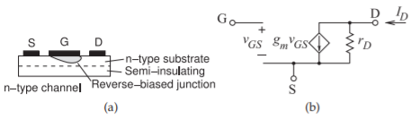
Figure \(\PageIndex{5}\): JFET details: (a) cross section; and (b) circuit model of fundamental operation.
the gate terminal. The term JFET most commonly refers to a silicon junction FET. With compound semiconductors such as GaAs, the pn junction of a silicon JFET is replaced by a Schottky barrier junction and the transistor is called a metal-epitaxy-semiconductor FET (MESFET). A device similar to the MESFET is the high electron mobility transistor (HEMT), where the field is established at the junction of two compound semiconductor materials having different band gaps, called a heterojunction. The channel is formed at the heterojunction. The HEMT is also called the heterostructure FET (HFET). A MESFET with a graded junction is called a modulation-doped FET (MODFET). A pseudomorphic HEMT (pHEMT) has an extremely thin layer establishing the channel so that the crystal structure stretches and a very high bandgap is established. Enhancement-mode and depletion-mode JFETs are contrasted in Figure \(\PageIndex{6}\).
The Materka-Kacprzak transistor model was developed for GaAs MESFET transistors [14] but is used to model silicon JFET and HEMT transistors as well. The model is described in Section 1.A.2 and the fundamental operation is described by Equation (1.A.44), which is repeated here without the area
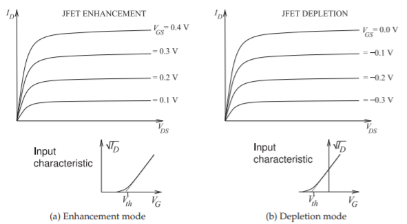
Figure \(\PageIndex{6}\): Current-voltage characteristics of depletion-mode and enhancement-mode JFETs.
multiplier:
\[\label{eq:20}I_{DS}=I_{DSS}\left[1+S_{S}\frac{V_{DS}}{I_{DSS}}\right]\left[1-\frac{V_{GS}(t-\tau )}{V_{P0}+\gamma V_{DS}}\right]^{(E+K_{E}V_{GS}(t-\tau ))}\times\tanh\left[\frac{S_{L}V_{DS}}{I_{DSS}(1-K_{G}V_{GS}(t-\tau ))}\right] \]
Here \(I_{DSS}\) is the drain saturation current, and this, along with all quantities in Equation \(\eqref{eq:20}\) other than \(V_{DS},\: V_{GS}\), and \(I_{DS}\) are constants and specified as inputs by the user. Equation \(\eqref{eq:20}\) indicates that the fundamental operation of a JFET is that of a voltage-controlled current source. Thus the small-signal circuit model of fundamental operation is as shown in Figure \(\PageIndex{5}\)(b).
The schematic symbols used for the MESFET, HEMT, and JFET are shown in Table \(\PageIndex{3}\). The only MESFET type used, however, is the n-type, as the ptype MESFET has poor performance due to the low mobility of holes.
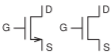
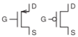
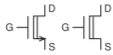
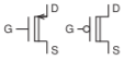
| Transistor | IEEE symbol | Commonly used symbol |
|---|---|---|
| FET, pJFET |  |
 |
| FET, nJFET, MESFET, HEMT |  |
 |
Table \(\PageIndex{3}\): IEEE standard schematic symbols for JFETs (MESFET, HEMT, JFET) [8] and symbols more commonly used in schematics. The letters indicate terminals: \(\mathsf{G}\) (gate), \(\mathsf{D}\) (drain), \(\mathsf{S}\) (source).
Footnotes
[1] A Schottky barrier occurs at the abrupt interface between a metal and a doped semiconductor.
[2] The discussion is similar for a pMOSFET, but with holes (p-type carriers) forming the channel.
[3] Mobility, \(\mu\), is the proportionality of the velocity of carriers to the applied electric field, \(v_{d} = \mu E\), where \(v_{d}\) is the average drift velocity of carriers and \(E\) is the applied electric field. Mobility has the units \(\text{m}^{2}/(\text{V}\cdot\text{s})\), i.e. \(\text{m}^{2}\cdot\text{V}^{−1}\cdot\text{s}^{−1}\).