
2.5: Class A, AB, B, and C Amplifiers
- Page ID
- 46027
Transistor amplifiers use several different biasing strategies. The strategies are identified as classes of amplifiers ranging from Class A to Class G. In this section Class A, AB, B, and C amplifiers are considered and these have the basic topologies of Figure 2.4.1, where input and output matching networks have been omitted. Class A–C amplifiers have the same impedance presented to the output of the amplifier at the operating frequency and at
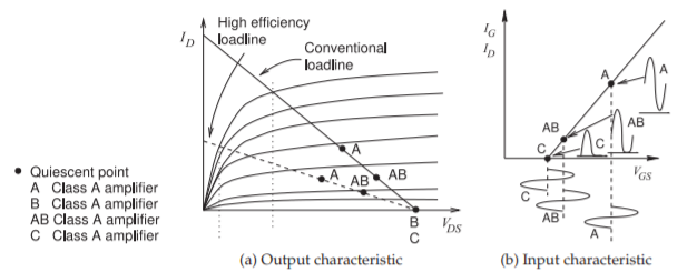
Figure \(\PageIndex{1}\): Current-voltage characteristics of a transistor used in an amplifier showing the quiescent points of various amplifier classes.
harmonics. Figure \(\PageIndex{1}\)(a) is the output characteristic of a transistor and shows the distinguishing quiescent points for the various classes of amplifier. The input characteristics are shown in Figure \(\PageIndex{1}\)(b), where the input (\(I_{G}\)) and output (\(I_{D}\)) current waveforms are shown for a sinusoidal input waveform (\(V_{GS}\)).
Amplifier design consists of both design for low-power linear operation, requiring maximum power transfer at the input and output of the amplifier, and a trade-off of acceptable distortion and efficiency. In practice, a certain level of distortion must be tolerated, and what is acceptable is embedded in the specifications of the various wireless systems.
For low distortion, the peaks of the RF signal must be amplified linearly, however, the DC power consumed depends on the amplifier class. With Class A amplifiers, the DC power must be sufficient to provide low-level distortion of the largest RF signal so that the DC power is proportional to the peak AC power.
The situation is similar for Class AB amplifiers, with the difference being that the intent is to accept some distortion of the peak signal so that the relationship between peak power and DC power still exists, but the direct proportionality no longer holds. For Class C and higher class amplifiers, the DC power is mostly proportional to the average RF power. So for Class A and Class AB amplifiers, the average operating point must be “backed off” to allow for manageable distortion of the peaks of a signal, with the level of back-off required being proportional to the PMEPR of the modulated signal. For Class C and higher classes, the back-off required comes from experience and experimentation. The characteristics of the signal also determine how much distortion can be tolerated.
The PMEPR of the signal is an indication of the type and amount of distortion that can be tolerated. The PMEPR of the two-tone signal is \(3\text{ dB}\), and digitally modulated signals can have PMEPRs ranging from \(0\text{ dB}\) to \(20\text{ dB}\) or more. A signal with a higher PMEPR results in lower efficiency, as more back-off is required. Putting this another way, the DC bias must be set so that there is minimum distortion when the signal is at its peak, but
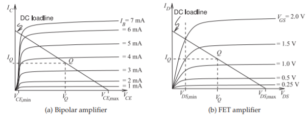
Figure \(\PageIndex{2}\): Current-voltage characteristics of transistor amplifiers shown with a Class A amplifier loadline: (a) bipolar amplifier; and (b) FET amplifier.
the average RF power produced can be much less than the peak RF power. (The average RF power is approximately an amount PMEPR below the peak RF power.) Thus for a high-PMEPR signal, generally a higher DC power is required to produce the same RF power. This is especially true for Class A amplifiers.
2.5.1 Class A Amplifier
The Class A amplifier has limited efficiency because there is always substantial quiescent current flowing whether or not RF current is flowing. Higher-order classes of amplifiers achieve higher efficiency, but distort the RF signal. The current and voltage loci of Class A, B, AB, and C amplifiers have a similar trajectory on the output current-voltage characteristics of a transistor. The output characteristics of a transistor are shown in Figure \(\PageIndex{1}\)(a), showing what is called the linear or DC loadline and the bias points for the various amplifier classes. The loadline is the locus of the DC current and voltage as the DC input voltage is varied.
With the Class A amplifier, the transistor is biased in the middle of the transistor characteristics, where the response has the highest linearity. That is, when the gate voltage varies due to an applied signal, the output voltage and current variations are nearly linearly proportional to the applied input. The drawback is that there is always considerable DC current flowing, even when the input signal is very small. That is, there is DC power consumption whether or not RF power is being generated at the output of the transistor. This is not of concern if small RF signals are to be amplified, as then a small transistor can be chosen so that the DC current levels are small. It is a problem if an amplifier must handle both large and small signals.
The Class A amplifier is defined by its ability to amplify small to medium and even large signals with minimal distortion. This is achieved by biasing a transistor in the middle of its \(I-V\) (i.e., current-voltage) characteristics. Figure \(\PageIndex{2}\) shows the \(I-V\) characteristics of the bipolar and FET transistors shown in Figure 2.4.1, together with the DC loadline. The loadline is the locus of the output current and voltage. For the Class A amplifiers in Figure 2.4.1(a and b)
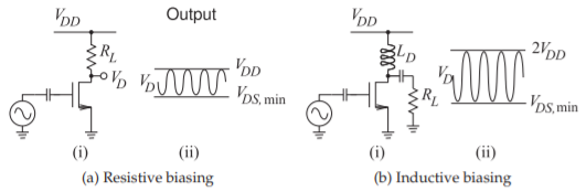
Figure \(\PageIndex{3}\): Single-ended Class A MOSFET amplifiers: (i) schematic; and (ii) drain voltage waveforms.
the loadlines are defined by
\[\label{eq:1}I_{C}=(V_{CC}-V_{CE})/R_{L}\quad\text{and}\quad I_{D}=(V_{DD}-V_{DS})/R_{L} \]
respectively. These are called single-ended amplifiers, as the input and output voltages are referred to ground. An amplifier using a bipolar transistor (either a BJT or an HBT), as shown in Figure 2.4.1(a), has the output characteristics shown in Figure \(\PageIndex{2}\)(a). Here the output voltage of the bipolar amplifier is \(V_{CE}\), and this swings from a maximum value of \(V_{CE\text{,max}}\) to a minimum of \(V_{CE\text{,min}}\). For a bipolar transistor \(V_{CE\text{,min}}\) is approximately \(0.2\text{ V}\), while \(V_{CE\text{,max}}\) for a resistively biased circuit is just the supply voltage, \(V_{CC}\). The quiescent or bias point is shown with collector-emitter voltage \(V_{Q}\) and quiescent current \(I_{Q}\). For a Class A amplifier, the quiescent point is just the bias point, and this is in the middle of the output voltage swing and the slope of the loadline is established by the load resistor, \(R_{L}\).
The output \(I-V\) characteristic of a FET amplifier is shown in Figure \(\PageIndex{2}\)(b). The notable difference between these characteristics and those of the bipolar transistor is that the curves are less abrupt at low output voltage (i.e., low \(V_{DS}\)). This results in the FET amplifier’s minimum output voltage, \(V_{DS\text{,min}}\), being larger than that of a BJT-based amplifier, \(V_{CE\text{,min}}\). For a typical RF FET amplifier, \(V_{DS\text{,min}}\) is \(0.5\text{ V}\).
The bipolar and FET amplifiers of Figure 2.4.1 use resistive biasing so that the maximum output voltage swing is limited. As well, the bias resistor is also the load resistor. Various alternative topologies have been developed yielding a range of output voltage swings. The common variations are shown in Figure \(\PageIndex{3}\) for a FET amplifier. Figure \(\PageIndex{3}\)(a) is a resistively biased Class A amplifier with the output voltage swing between \(V_{DS\text{,min}}\) and \(V_{DD}\). The quiescent drain-source voltage is halfway between these extremes. The load, \(R_{L}\), also provides correct biasing. A more efficient Class A amplifier uses inductive biasing, as shown in Figure \(\PageIndex{3}\)(b). Bias current is now provided via the drain inductor, and the load, \(R_{L}\), is not part of the bias circuit. With the inductively loaded Class A amplifier, the quiescent voltage is \(V_{DD}\) and the output voltage swing is between \(V_{DS\text{,min}}\) and \(2V_{DD}\), slightly more than twice the voltage swing of the resistively loaded amplifier.
A Class A amplifier can be designed using the \(S\) parameters of the transistor in a specific configuration. Ideally the effect of bias circuitry would be included in the \(S\) parameters of the transistor, but bias circuit
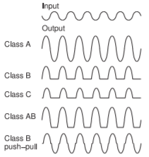
Figure \(\PageIndex{4}\): Input and output waveforms for various classes of amplifier.
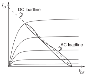
Figure \(\PageIndex{5}\): DC and RF loadlines of Class A, B, and C amplifiers. The AC loadline is also called the dynamic loadline.
design attempts to present RF open or short circuits as required to minimize impact on RF performance. Generally design begins with the transistor’s \(S\) parameters and assuming no bias circuit impact.
2.5.2 Amplifier Efficiency
Since the Class A amplifier is always drawing DC current, its efficiency is near zero when the input signal is very small. The maximum efficiency of Class A amplifiers is \(25\%\) if resistive biasing is used and \(50\%\) when inductive biasing is used. Efficiency is improved by reducing the DC power, and this is achieved by moving the bias point further down the DC loadline, as in the Class B, AB, and C amplifiers shown in Figure \(\PageIndex{1}\). Reducing the bias results in signal distortion for large RF signals. This can be seen in the various output waveforms shown in Figure \(\PageIndex{4}\). Class A amplifiers have the highest linearity and Class B and C amplifiers result in considerable distortion. As a compromise, Class AB amplifiers are used in many cellular applications, although Class C amplifiers are used with constant envelope modulation schemes, as in GSM. Nearly all small-signal amplifiers are Class A.
The effect of parasitic capacitances and delay effects (such as those due to the time it takes carriers to move across a base for a BJT or under the gate for a FET) result in the current-voltage locus for RF signals differing from the DC situation. This effect is captured by the dynamic or AC loadline, which is shown in Figure \(\PageIndex{5}\).
The Class A amplifier is a low-efficiency, but highly linear class. The other amplifier classes have higher efficiencies but varying degrees of distortion, as seen in Figure \(\PageIndex{4}\). The output of the Class B amplifier contains an amplified version of only half of the input signal but draws just a small leakage current when no signal is applied. With the Class C amplifier there must be some positive RF input signal before there is an output: there is more distortion but no current flows, not even leakage current, when there is no RF input signal. The Class AB amplifier is a compromise between Class A and Class B amplifiers. Less DC current flows than with Class A when there is negligible input signal, and the distortion is less than with Class B. Filtering, often provided by matching networks, eliminates harmonics from the output of the amplifier, but in-band distortion of finite bandwidth signals remains.
Class C amplifiers are biased so that there is almost no drain-source (or collector-emitter) current when no RF signal is applied, so the output waveform has considerable distortion, as shown in Figure \(\PageIndex{4}\). This distortion is important only if there is information in the amplitude of the signal. FM, PM, and to a lesser extent GMSK schemes result in signals with constant (or for GMSK near constant) RF envelopes, thus there is no information contained in the amplitude of the signal. Therefore errors introduced into the amplitude of a signal are of lesser significance and efficient saturating mode amplifiers such as a Class C amplifier can be used. In contrast, PSK and QAM modulation schemes do not result in signals with constant RF envelopes and so some information is contained in the amplitude of the RF signal. For these modulation techniques, reasonably linear amplifiers are required.
The Class A amplifier presents input and output impedances that are almost independent of the level of the signal. However, a Class B, AB, or C amplifier presents input and output impedances that vary depending on the level of the RF signal. Thus design requires more care, as the chances of instability are higher and it is more likely that an oscillation condition will be met. Also, Class B, AB, and C amplifiers are generally not used in broadband applications or at high frequencies (say above \(20\text{ GHz}\)) mainly because of the problem of maintaining stability. Class A amplifiers are then the preferred solution as design is simpler and the amplifier is more tolerant of parasitic effects and variations.
Example \(\PageIndex{1}\): Efficiency of a Class A Amplifier
Determine the efficiency of a Class A FET amplifier with resistive biasing using the FET characteristics shown in Figure \(\PageIndex{2}\)(b).
Solution
For maximum output voltage swing, the quiescent point should be halfway between the maximum and minimum drain source voltages,
\[\label{eq:2}V_{O}=V_{DS,\text{min}}+\left(\frac{V_{DS,\text{max}}-V_{DS,\text{min}}}{2}\right)=\left(\frac{V_{DD}+V_{DS,\text{min}}}{2}\right) \]
since \(V_{DS\text{,max}} = V_{DD}\). The quiescent (DC) current through \(R_{L}\) is
\[\label{eq:3}I_{Q}=\frac{V_{DD}-V_{O}}{R_{L}}=\left(V_{DD}-\frac{V_{DD}+V_{DS,\text{min}}}{2}\right)\frac{1}{R_{L}}=\frac{V_{DD}-V_{DS,\text{min}}}{2R_{L}} \]
and the quiescent (DC) power consumed is
\[\label{eq:4}P_{DC}=V_{DD}I_{Q}=V_{DD}\left(\frac{V_{DD}-V_{DS,\text{min}}}{2R_{L}}\right)=\frac{V_{DD}^{2}}{2R_{L}}\left(1-\frac{V_{DS,\text{min}}}{V_{DD}}\right) \]
The peak voltage of the AC output is
\[\label{eq:5}V_{p}=(V_{DD}-V_{DS,\text{min}})/2 \]
so that the RF output power in the load is
\[\label{eq:6}P_{RF,\text{out}}=\frac{1}{2}\left(\frac{V_{DD}-V_{DS,\text{min}}}{2}\right)^{2}\frac{1}{R_{L}}=\frac{V_{DD}^{2}}{8R_{L}}\left(1-\frac{V_{DS,\text{min}}}{V_{DD}}\right)^{2} \]
Thus the efficiency of the amplifier is
\[\label{eq:7}\eta=\frac{P_{RF,\text{out}}}{P_{DC}}=\frac{1}{4}\left(1-\frac{V_{DS,\text{min}}}{V_{DD}}\right) \]
If the minimum drain voltage is ignored (\(V_{DS\text{,min}} = 0\)), then \(\eta = 1/4 = 25\%\). This is the maximum efficiency of a resistively biased Class A amplifier.
Figure \(\PageIndex{6}\): A two-port network with inputs at the source and load used in defining stability measures: (a) network; (b) input signal flow graph; and (c) output signal flow graph.