
2.9: Case Study- Narrowband Linear Amplifier Design
- Page ID
- 46031
The design procedure for linear amplifiers is well developed and the strategy forms the basis for all amplifier design. An amplifier has three major components: an input matching network, an active device, and an output matching network (see Figure \(\PageIndex{1}\)). There are a number of design choices to be made and these will be illustrated by considering the design of an amplifier for maximum gain using the discrete pHEMT transistor examined previously (see Table 2.3.1). The design specifications are
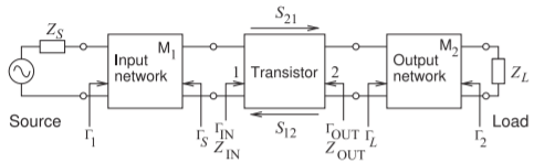
Figure \(\PageIndex{1}\): Linear amplifier comprising input and output matching networks and an active device in a specific configuration forming a two-port.
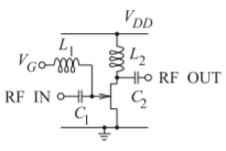
Figure \(\PageIndex{2}\): Bias configuration for pHEMT amplifier. \(L_{1}\) and \(L_{2}\) are RF chokes and large enough to block RF. \(C_{1}\) and \(C_{2}\) are DC blocking capacitors that block DC but allow RF to pass with negligible impedance.
\[\begin{array}{ll}{\text{Gain:}}&{\text{maximum gain at }8\text{ GHz}} \\ {\text{Topology:}}&{\text{three two-ports (input and output matching}}\\{}&{\text{networks, and the active device)}}\\{\text{Stability:}}&{\text{broadband stability}}\\{\text{Bandwidth:}}&{\text{maximum that can be achieved using two-}}\\{}&{\text{element matching networks}}\\{\text{Source impedance:}}&{Z_{S}=50\:\Omega}\\{\text{Load impedance:}}&{Z_{L}=50\:\Omega}\end{array}\nonumber \]
2.9.1 Bias Circuit Topology
The first design step is to choose a biasing configuration, and this is directly related to the output voltage swing supported. The inductively biased configuration in Figure \(\PageIndex{2}\) will be used. Here \(L_{1}\) and \(L_{2}\) are RF chokes and large enough to block RF. \(C_{1}\) and \(C_{2}\) are DC blocking capacitors that block DC but allow RF to pass with negligible impedance. The input matching network is attached to the RF IN terminal and the output matching network is attached to the RF OUT terminal. \(V_{DD}\) is the supply voltage and \(V_{G}\) is the DC gate voltage typically provided by an analog integrated circuit available in conjunction with most RF designs. An additional design objective is to absorb the biasing circuit into the matching networks.
2.9.2 Stability Considerations
It is not sufficient to consider a single frequency in design, as stability must be ensured at low and high frequencies. The stability factor of the active device was given in Table 2.6.2. This indicates that the device is unconditionally stable from \(5\) to \(11\text{ GHz}\) and from \(22\) to \(26\text{ GHz}\). At the high-frequency end, the gain of the device reduces rapidly with increasing frequency as the capacitive parasitics begin dominating transmission through the device. Therefore it is reasonable to assume that the device is unconditionally stable above \(22\text{ GHz}\).
Design nearly always commences with the output matching network. The first design step is to choose a matching network that will provide the appropriate impedances to ensure stability below \(5\text{ GHz}\) and above \(11\text{ GHz}\). To do this the stability circles must be considered, as the device is only conditionally stable at these frequencies. The center and radius of the input and output stability circles are listed in Table 2.6.1. These are plotted in Figure \(\PageIndex{3}\) for selected frequencies.
2.9.3 Output Matching Network Design
The output stability circle at \(1\text{ GHz}\) (see Figure \(\PageIndex{3}\)(a)) indicates that for stable, low-frequency amplification, the output matching network, as seen from the transistor, could look like a short circuit, a matched load, or a capacitor at low frequencies. Figure \(\PageIndex{3}\)(c), the output stability circle at
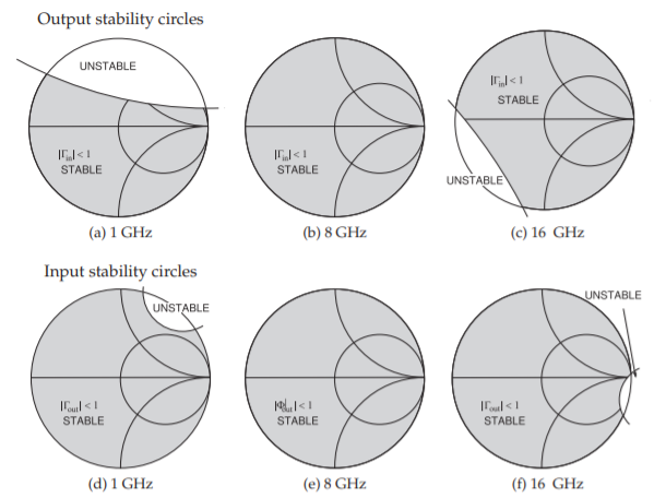
Figure \(\PageIndex{3}\): Input and output stability circles on the complex reflection coefficient planes for \(|S_{11}| < 1\) and \(|S_{22}| < 1\).
Figure \(\PageIndex{4}\): Output matching network candidates required for out-of-band stability. The active device is on the left.
\(16\text{ GHz}\), indicates that for stable, high-frequency amplification the output matching network, as seen from the transistor, could look like an open circuit or a matched load at high frequencies. As expected, the output stability circle at \(8\text{ GHz}\) (see Figure \(\PageIndex{3}\)(b)) indicates unconditional stability. Examining the two-element matching networks in Figure 6-7 of [2], there are three candidate output matching networks that are shown in Figure \(\PageIndex{4}\).
From Table 2.3.1, the device \(S\) parameters at \(8\text{ GHz}\) are as follows:
\[\begin{array}{ll}{S_{11}=0.486\angle 140.4^{\circ}}&{S_{21}=3.784\angle 11.2^{\circ}} \\{S_{12}=0.057\angle 6.4^{\circ}}&{S_{22}=0.340\angle -99.1^{\circ}}\end{array}\nonumber \]
To start, ignore \(S_{12}\) so that \(\Gamma_{\text{OUT}} = S_{22} = 0.340\angle −99.1\). There is little choice here as \(\Gamma_{\text{OUT}}\) depends on the input matching network that has not yet been designed. It would have been possible to begin with the input matching network and make this approximation for \(\Gamma_{\text{IN}}\). However, experience is that the error introduced by starting with the output matching network is less. Once the output matching network has been designed, \(\Gamma_{\text{IN}}\) can be calculated without approximation. A thorough design would complete the first pass of the design and then make one more pass without the approximation that ignores \(S_{12}\). Now, with \(\Gamma_{\text{OUT}} = S_{22}\), the output impedance of the active device is
\[\begin{align}Z_{\text{OUT}}&=Z_{0}\frac{1+\Gamma_{\text{OUT}}}{1-\Gamma_{\text{OUT}}}=Z_{0}\frac{1+S_{22}}{1-S_{22}}\nonumber \\ &=(50\:\Omega )\frac{1+(0.340\angle -99.1^{\circ})}{1-(0.340\angle -99.1^{\circ})}=(50\:\Omega)\frac{1+(-0.053774-\jmath 0.335721)}{1-(-0.053774 - \jmath 0.335721)}\nonumber \\ \label{eq:1}&=36.153-\jmath 27.447\:\Omega\end{align} \]
or \(Y_{\text{OUT}} = 1/Z_{\text{OUT}} = 0.017547 + \jmath 0.013322\text{ S}\). The output of the active device looks like a \(56.99\:\Omega\) resistor in parallel with a capacitor with a reactance of \(−75.064\:\Omega\). So taking into account the bias objectives and the available output matching networks in Figure \(\PageIndex{4}\), the matching network topology of Figure \(\PageIndex{4}\)(c) will be used where the source in the matching network is the active device. So the output matching network problem is as shown in Figure \(\PageIndex{5}\). This choice enables the inductor to be used to apply bias.
The complete output matching problem is shown in Figure \(\PageIndex{5}\)(a). In part, the parallel configuration of the active device output impedance was chosen, as this is closer to reality since there is a capacitance at the output of the transistor. Resonance, as shown in Figure \(\PageIndex{5}\)(b), will be used to cancel the effect of the active device capacitance, so that the matching problem reduces to that shown in Figure \(\PageIndex{5}\)(c). Using the procedure outlined in Section 6.4.2 of [2],
\[\label{eq:2}|Q_{S}|=|Q_{P}|=\sqrt{\frac{R_{S}}{R_{L}}-1}=\sqrt{\frac{56.99}{50}-1}=0.3739 \]
\[\label{eq:3}Q_{S}=\left|\frac{X_{S}}{R_{L}}\right| = \left|\frac{X_{S}}{50\:\Omega}\right|=0.3739\text{ and }Q_{P}=\left|\frac{R_{S}}{X_{P}}\right|=\left|\frac{56.99\:\Omega}{X_{P}}\right|=0.3739 \]
so
\[\label{eq:4}X_{S}=-18.70\:\Omega\quad\text{and}\quad X_{P}=152.4\:\Omega \]
Now \(X_{x} = −75.064\:\Omega\), so \(75.064\:\Omega\) must be added to \(X_{P}\) in parallel, and the reactance of \(L_{o}\) is \(50.29\:\Omega\), thus (at \(8\text{ GHz}\))
\[\label{eq:5}L_{o}=1.00\text{ nH}\quad\text{and}\quad C_{o}=1.064\text{ pF} \]
The final output matching network design is shown in Figure \(\PageIndex{5}\)(d).
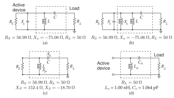
Figure \(\PageIndex{5}\): Steps in the design of the output matching network: (a) active device presents itself as a resistance in parallel with a capacitive reactance to the output matching network; (b) with inductor to resonate out active device reactance; (c) simplified matching network problem; and (d) final output matching network design.
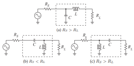
Figure \(\PageIndex{6}\): Input matching network candidates required for out-of-band stability. The active device is on the right.)
2.9.4 Input Matching Network Design
The input stability circle at \(1\text{ GHz}\) (Figure \(\PageIndex{3}\)(d)) indicates that at \(1\text{ GHz}\), the input matching network, as seen from the transistor, could look like a short circuit, a matched load, or a capacitor at low frequencies. Figure \(\PageIndex{3}\)(f), the input stability circle at \(16\text{ GHz}\), indicates that the input matching network, as seen from the transistor, could look like a short circuit or a matched load at high frequencies. Examining the two-element matching networks in Figure 6-7 of [2], there are three candidate input matching networks as shown in Figure \(\PageIndex{6}\).
The reflection coefficient looking into the output matching network from the active device is \(\Gamma_{L} = S_{22}^{\ast} = 0.340\angle 99.1^{\circ}\) because of the design decision to ignore \(S_{12}\) for the output matching network. Now that the output matching
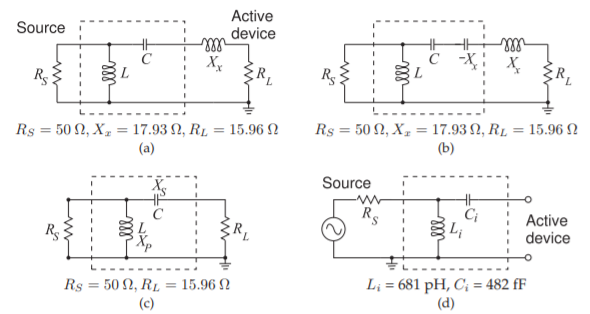
Figure \(\PageIndex{7}\): Steps in the design of the input matching network: (a) active device presents itself as a resistance in series with an inductive reactance to the input matching network; (b) with a capacitor to resonate out the active device reactance; (c) simplified matching network problem; and (d) final output matching network design.
network has been designed, the feedback parameter need no longer be ignored. So
\[\begin{align}\label{eq:6}\Gamma_{\text{IN}}&=S_{11}+\frac{S_{12}S_{21}\Gamma_{L}}{1-S_{22}\Gamma_{L}} \\ \label{eq:7}&=(0.486\angle 140.4^{\circ})+\frac{(0.057\angle 6.4^{\circ})(3.784\angle 11.2^{\circ})(0.340\angle 99.1^{\circ})}{1− (0.340\angle −99.1^{\circ})(0.340\angle 99.1^{\circ})} \\ \label{eq:8}&=-0.4117+\jmath 0.3839\end{align} \]
That is, \(Z_{\text{IN}} = 15.959 +\jmath 17.935\:\Omega\). So taking into account the bias objectives and the output matching networks shown in Figure \(\PageIndex{6}\), the matching network topology of Figure \(\PageIndex{6}\)(c) will be used (where the load is the active device). The input matching network problem is as shown in Figure \(\PageIndex{7}\)(c). (Biasing cannot be incorporated into this matching network.) Now
\[\begin{align}\label{eq:9}|Q_{S}|&=|Q_{P}|=\sqrt{\frac{R_{S}}{R_{L}}-1}=\sqrt{\frac{50}{15.959}-1}=1.4605 \\ \label{eq:10}Q_{S}&=\left|\frac{X_{S}}{R_{L}}\right|=\left|\frac{X_{S}}{15.959\:\Omega}\right|=1.4605\quad\text{and}\quad Q_{P}=\left|\frac{R_{S}}{X_{P}}\right|=\left|\frac{50\:\Omega}{X_{P}}\right|=1.4605\end{align} \]
So
\[\label{eq:11}X_{S}=-23.31\:\Omega\quad\text{and}\quad X_{P}=34.23\:\Omega \]
Since \(X_{x} = 17.935\:\Omega\), \(−17.935\:\Omega\) must be added to \(X_{S}\), and the reactance of \(C_{i}\) is \(41.24\:\Omega\), thus (at \(8\text{ GHz}\)),
\[\label{eq:12}L_{i}=681\text{ pH}\quad\text{and}\quad C_{i}=482\text{ fF} \]
The final input matching network design is shown in Figure \(\PageIndex{5}\)(d).
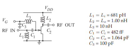
Figure \(\PageIndex{8}\): Final amplifier schematic.
2.9.5 Bias Network Design
The final schematic of the linear amplifier design is shown in Figure \(\PageIndex{8}\). The output matching network, \(L_{2}\) and \(C_{2}\), enabled the biasing inductor to be replaced by \(L_{2}\). So the output bias circuitry is absorbed into the output matching network. A similar result is not obtained with the input matching network, \(L_{1}\) and \(C_{1}\). A separate gate bias network is still required. \(L_{3}\) should be a large enough value for it to act as an RF choke. A value of \(10\text{ nH}\) provides a reactance of approximately \(500\:\Omega\) at \(8\text{ GHz}\). The value of \(C_{3} = 100\text{ pF}\) is chosen large enough to provide an RF short and stabilize the DC bias, \(V_{G}\). This is a surprisingly simple circuit that provides maximum gain at \(8\text{ GHz}\), ensures out-of-band stability, and provides DC bias. Another design iteration with a more sophisticated input matching network may enable the separate bias inductor \(L_{3}\) to be eliminated. As it is, the gate bias circuit further ensures stability at low frequencies, as then the gate tends to be shorted out. The amplifier has a calculated transducer gain of \(13.2\text{ dB}\), which can be compared to the gains reported in Table 2.3.3, where gain metrics were determined with \(S_{12}\) ignored.
Linear amplifier design for a specific gain is also possible. Now the errors involved in ignoring \(S_{12}\) during the design process are significant and a full bilateral treatment is required. This design approach is described in references [11, 27, 28].