3.7: Case Study- Distributed Biasing of Differential Amplifiers
- Page ID
- 46043
\( \newcommand{\vecs}[1]{\overset { \scriptstyle \rightharpoonup} {\mathbf{#1}} } \)
\( \newcommand{\vecd}[1]{\overset{-\!-\!\rightharpoonup}{\vphantom{a}\smash {#1}}} \)
\( \newcommand{\id}{\mathrm{id}}\) \( \newcommand{\Span}{\mathrm{span}}\)
( \newcommand{\kernel}{\mathrm{null}\,}\) \( \newcommand{\range}{\mathrm{range}\,}\)
\( \newcommand{\RealPart}{\mathrm{Re}}\) \( \newcommand{\ImaginaryPart}{\mathrm{Im}}\)
\( \newcommand{\Argument}{\mathrm{Arg}}\) \( \newcommand{\norm}[1]{\| #1 \|}\)
\( \newcommand{\inner}[2]{\langle #1, #2 \rangle}\)
\( \newcommand{\Span}{\mathrm{span}}\)
\( \newcommand{\id}{\mathrm{id}}\)
\( \newcommand{\Span}{\mathrm{span}}\)
\( \newcommand{\kernel}{\mathrm{null}\,}\)
\( \newcommand{\range}{\mathrm{range}\,}\)
\( \newcommand{\RealPart}{\mathrm{Re}}\)
\( \newcommand{\ImaginaryPart}{\mathrm{Im}}\)
\( \newcommand{\Argument}{\mathrm{Arg}}\)
\( \newcommand{\norm}[1]{\| #1 \|}\)
\( \newcommand{\inner}[2]{\langle #1, #2 \rangle}\)
\( \newcommand{\Span}{\mathrm{span}}\) \( \newcommand{\AA}{\unicode[.8,0]{x212B}}\)
\( \newcommand{\vectorA}[1]{\vec{#1}} % arrow\)
\( \newcommand{\vectorAt}[1]{\vec{\text{#1}}} % arrow\)
\( \newcommand{\vectorB}[1]{\overset { \scriptstyle \rightharpoonup} {\mathbf{#1}} } \)
\( \newcommand{\vectorC}[1]{\textbf{#1}} \)
\( \newcommand{\vectorD}[1]{\overrightarrow{#1}} \)
\( \newcommand{\vectorDt}[1]{\overrightarrow{\text{#1}}} \)
\( \newcommand{\vectE}[1]{\overset{-\!-\!\rightharpoonup}{\vphantom{a}\smash{\mathbf {#1}}}} \)
\( \newcommand{\vecs}[1]{\overset { \scriptstyle \rightharpoonup} {\mathbf{#1}} } \)
\( \newcommand{\vecd}[1]{\overset{-\!-\!\rightharpoonup}{\vphantom{a}\smash {#1}}} \)
\(\newcommand{\avec}{\mathbf a}\) \(\newcommand{\bvec}{\mathbf b}\) \(\newcommand{\cvec}{\mathbf c}\) \(\newcommand{\dvec}{\mathbf d}\) \(\newcommand{\dtil}{\widetilde{\mathbf d}}\) \(\newcommand{\evec}{\mathbf e}\) \(\newcommand{\fvec}{\mathbf f}\) \(\newcommand{\nvec}{\mathbf n}\) \(\newcommand{\pvec}{\mathbf p}\) \(\newcommand{\qvec}{\mathbf q}\) \(\newcommand{\svec}{\mathbf s}\) \(\newcommand{\tvec}{\mathbf t}\) \(\newcommand{\uvec}{\mathbf u}\) \(\newcommand{\vvec}{\mathbf v}\) \(\newcommand{\wvec}{\mathbf w}\) \(\newcommand{\xvec}{\mathbf x}\) \(\newcommand{\yvec}{\mathbf y}\) \(\newcommand{\zvec}{\mathbf z}\) \(\newcommand{\rvec}{\mathbf r}\) \(\newcommand{\mvec}{\mathbf m}\) \(\newcommand{\zerovec}{\mathbf 0}\) \(\newcommand{\onevec}{\mathbf 1}\) \(\newcommand{\real}{\mathbb R}\) \(\newcommand{\twovec}[2]{\left[\begin{array}{r}#1 \\ #2 \end{array}\right]}\) \(\newcommand{\ctwovec}[2]{\left[\begin{array}{c}#1 \\ #2 \end{array}\right]}\) \(\newcommand{\threevec}[3]{\left[\begin{array}{r}#1 \\ #2 \\ #3 \end{array}\right]}\) \(\newcommand{\cthreevec}[3]{\left[\begin{array}{c}#1 \\ #2 \\ #3 \end{array}\right]}\) \(\newcommand{\fourvec}[4]{\left[\begin{array}{r}#1 \\ #2 \\ #3 \\ #4 \end{array}\right]}\) \(\newcommand{\cfourvec}[4]{\left[\begin{array}{c}#1 \\ #2 \\ #3 \\ #4 \end{array}\right]}\) \(\newcommand{\fivevec}[5]{\left[\begin{array}{r}#1 \\ #2 \\ #3 \\ #4 \\ #5 \\ \end{array}\right]}\) \(\newcommand{\cfivevec}[5]{\left[\begin{array}{c}#1 \\ #2 \\ #3 \\ #4 \\ #5 \\ \end{array}\right]}\) \(\newcommand{\mattwo}[4]{\left[\begin{array}{rr}#1 \amp #2 \\ #3 \amp #4 \\ \end{array}\right]}\) \(\newcommand{\laspan}[1]{\text{Span}\{#1\}}\) \(\newcommand{\bcal}{\cal B}\) \(\newcommand{\ccal}{\cal C}\) \(\newcommand{\scal}{\cal S}\) \(\newcommand{\wcal}{\cal W}\) \(\newcommand{\ecal}{\cal E}\) \(\newcommand{\coords}[2]{\left\{#1\right\}_{#2}}\) \(\newcommand{\gray}[1]{\color{gray}{#1}}\) \(\newcommand{\lgray}[1]{\color{lightgray}{#1}}\) \(\newcommand{\rank}{\operatorname{rank}}\) \(\newcommand{\row}{\text{Row}}\) \(\newcommand{\col}{\text{Col}}\) \(\renewcommand{\row}{\text{Row}}\) \(\newcommand{\nul}{\text{Nul}}\) \(\newcommand{\var}{\text{Var}}\) \(\newcommand{\corr}{\text{corr}}\) \(\newcommand{\len}[1]{\left|#1\right|}\) \(\newcommand{\bbar}{\overline{\bvec}}\) \(\newcommand{\bhat}{\widehat{\bvec}}\) \(\newcommand{\bperp}{\bvec^\perp}\) \(\newcommand{\xhat}{\widehat{\xvec}}\) \(\newcommand{\vhat}{\widehat{\vvec}}\) \(\newcommand{\uhat}{\widehat{\uvec}}\) \(\newcommand{\what}{\widehat{\wvec}}\) \(\newcommand{\Sighat}{\widehat{\Sigma}}\) \(\newcommand{\lt}{<}\) \(\newcommand{\gt}{>}\) \(\newcommand{\amp}{&}\) \(\definecolor{fillinmathshade}{gray}{0.9}\)In this case study a broadband distributed balun-like section is presented as an alternative to inductor-biasing of a pseudo-differential amplifier (PDA). The distributed biasing circuit discriminates between differential-and common-mode signals, resulting in rejection of common-mode signals. A PDA is shown in Figure \(\PageIndex{1}\), where the inductors present high RF impedances to the transistors while providing low-impedance paths for bias currents. However, inductive biasing of pseudo-differential circuits presents the same environment to common- and differential-mode signals so that the CMRR is \(1\).
Differential amplifiers have large differential gain, \(A_{d}\). At the same time it is desirable to minimize the common-mode gain, \(A_{c}\), as the resulting high CMRR provides immunity to substrate-induced noise. Considering that each transistor has transconductance, \(g_{m}\), and that even- and odd-mode impedances, \(Z_{\text{EVEN}}\) and \(Z_{\text{ODD}}\), are presented to the drains of the transistors, then the gains are approximately
\[\label{eq:1}A_{d}=g_{m}Z_{\text{ODD}}\quad\text{and}\quad A_{c}=g_{m}Z_{\text{EVEN}} \]
and so
\[\label{eq:2}\text{CMRR}=A_{d}/A_{c}=Z_{\text{ODD}}/Z_{\text{EVEN}} \]
The desired amplifier characteristics are thus obtained by synthesizing the even- and odd-mode impedances.
First consider the inductively biased circuit in Figure \(\PageIndex{1}\). Modal analysis of the inductor biasing circuit results in the circuit model shown in Figure \(\PageIndex{2}\), from which the total even-mode impedance is
\[\label{eq:3}Z_{\text{EVEN}}(s)=(s_{L}+R_{DD}/2)//R_{L} \]
where \(//\) indicates a parallel connection, and the total odd-mode impedance is
\[\label{eq:4}Z_{\text{ODD}}(s)=sL//R_{L} \]
Since \(R_{DD}\) is usually negligible and \(L\) is a bias or choke inductor so that \(sL\) is very large, \(Z_{\text{ODD}}\approx R_{D}\approx Z_{\text{EVEN}}\) and so the CMRR is \(1\). However, a coupled-line network can provide different model impedances.
Now consider the Marchand balun-like structure in Figure \(\PageIndex{3}\) that replaces the drain bias circuit in Figure \(\PageIndex{1}\). The Marchand Balun structure
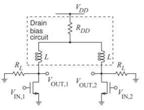
Figure \(\PageIndex{1}\): A PDA amplifier with bias inductors, \(L\), at the drains, parasitic supply resistance, \(R_{DD}\), and single-ended load impedance, \(R_{L}\). \(L\) is also known as a choke inductor chosen so that its impedance is very large at the maximum operating frequency, i.e. \(|sL| ≫ R_{L}\).
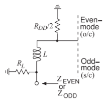
Figure \(\PageIndex{2}\): Modal subcircuits of the inductor-based biasing circuit of Figure \(\PageIndex{1}\), including single-ended load resistance \(R_{L}\).
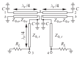
Figure \(\PageIndex{3}\): Marchand balun-like biasing circuit with single-ended load resistance \(R_{L}\). External DC bias is applied at Ports \(b\) using decoupling capacitors to ensure RF ground.
presents different impedances for common- and differential-mode signals. The synthesis of this biasing circuit is described in [8, 9] and follows a procedure similar to that for filter design. So high CMRR performance is the result of presenting different even- and odd-mode impedances to the active devices. The final results of the design are shown in Figure 3.8.1, first for inductive-biasing of the PDA and then for the coupled-line balun-like biasing circuit.