
3.11: Exercises
- Page ID
- 46033
\( \newcommand{\vecs}[1]{\overset { \scriptstyle \rightharpoonup} {\mathbf{#1}} } \) \( \newcommand{\vecd}[1]{\overset{-\!-\!\rightharpoonup}{\vphantom{a}\smash {#1}}} \)\(\newcommand{\id}{\mathrm{id}}\) \( \newcommand{\Span}{\mathrm{span}}\) \( \newcommand{\kernel}{\mathrm{null}\,}\) \( \newcommand{\range}{\mathrm{range}\,}\) \( \newcommand{\RealPart}{\mathrm{Re}}\) \( \newcommand{\ImaginaryPart}{\mathrm{Im}}\) \( \newcommand{\Argument}{\mathrm{Arg}}\) \( \newcommand{\norm}[1]{\| #1 \|}\) \( \newcommand{\inner}[2]{\langle #1, #2 \rangle}\) \( \newcommand{\Span}{\mathrm{span}}\) \(\newcommand{\id}{\mathrm{id}}\) \( \newcommand{\Span}{\mathrm{span}}\) \( \newcommand{\kernel}{\mathrm{null}\,}\) \( \newcommand{\range}{\mathrm{range}\,}\) \( \newcommand{\RealPart}{\mathrm{Re}}\) \( \newcommand{\ImaginaryPart}{\mathrm{Im}}\) \( \newcommand{\Argument}{\mathrm{Arg}}\) \( \newcommand{\norm}[1]{\| #1 \|}\) \( \newcommand{\inner}[2]{\langle #1, #2 \rangle}\) \( \newcommand{\Span}{\mathrm{span}}\)\(\newcommand{\AA}{\unicode[.8,0]{x212B}}\)
- Consider a \(Z_{0} = 50\:\Omega\) transmission line of length \(\lambda /10\) at \(30\text{ GHz}\).
- Calculate the \(ABCD\) parameters of the transmission line at \(30\text{ GHz}\)?
- With the transmission line shunted by \(0.05\text{ pF}\) capacitors at each end, calculate the \(ABCD\) parameters of the augmented transmission line.
- At \(30\text{ GHz}\) the augmented transmission line is equivalent to a single transmission line with characteristic impedance \(Z_{01}\) and length \(\ell_{1}\). What is \(\ell_{1}\) in terms of wavelengths?
- What is \(Z_{01}\)?
- A four-stage distributed FET amplifier as shown in Figure 3.2.1 has \(R_{S} = R_{L} = 50\:\Omega\). If the capacitive and resistive loading of the transistors are ignored, what are the optimum values of \(R_{1}\) and \(R_{2}\)? Provide your reasoning.
- The four-stage distributed FET amplifier shown in Figure 3.2.1 has \(R_{S} = 80\:\Omega\) and \(R_{L} = 25\:\Omega\). If the capacitive and resistive loading of the transistors are ignored, what are the optimum values of \(R_{1}\) and \(R_{2}\)? Provide your reasoning.
- The input matching network of the wideband amplifier considered in Section 3.5 is shown in Figure 3.5.9(b). (Note that Port 2 of the input network is connected to the transistor.) Typically the complex conjugate of \(S_{22}\) of the input network would match the input reflection coefficient, \(\Gamma_{\text{in}}\), of the transistor. Put your answers in magnitude-angle form.
- Draw the input matching network showing where \(S_{22}\) is determined. Also draw the transistor terminated by the output matching network and indicate where \(\Gamma_{\text{in}}\) is calculated.
- Use a microwave simulator to calculate the \(S_{22}\) of the input matching network at \(8, 9, ..., 12\text{ GHz}\).
- Determine \(S_{22}^{\ast}\) of the input matching network at \(8, 9, ..., 12\text{ GHz}\).
- Determine \(S_{11}\) of the transistor at \(8, 9, ..., 12\text{ GHz}\).
- Determine \(\Gamma_{\text{in}}\) of the transistor (terminated in the output matching network) at \(8, 9, ..., 12\text{ GHz}\).
- On a Smith chart plot \(S_{22}^{\ast}\) of the input network, \(S_{11}\) of the transistor, and \(\Gamma_{\text{in}}\) of the transistor.
- Describe the input matching network condition for maximum power transfer used in narrowband amplifier design.
- Discuss the mismatch of \(\Gamma_{\text{in}}\) of the transistor and \(S_{22}^{\ast}\) of the input matching network. Describe the effect that this has on the broadband response of the amplifier.
- The output matching network of the wideband amplifier considered in Section 3.5 is shown in Figure 3.5.10(b). (Note that Port 2 of the input network is connected to the transistor.) Typically the complex conjugate of \(S_{22}\) of the output network would match the input reflection coefficient, \(\Gamma_{\text{out}}\), of the transistor. Put your answers in magnitude-angle form.
- Draw the output matching network showing where \(S_{22}\) is determined. Also draw the transistor terminated by the input matching network and indicate where \(\Gamma_{\text{out}}\) is calculated.
- Use a microwave simulator to calculate the \(S_{22}\) of the output matching network at \(8, 9, ..., 12\text{ GHz}\).
- Determine \(S_{22}^{\ast}\) of the output matching network at \(8, 9, ..., 12\text{ GHz}\).
- Determine \(S_{22}\) of the transistor at \(8, 9, ..., 12\text{ GHz}\).
- Determine \(\Gamma_{\text{out}}\) of the transistor (terminated in the output matching network) at \(8, 9, ..., 12\text{ GHz}\).
- On a Smith chart plot \(S_{22}^{\ast}\) of the output network, \(S_{22}\) of the transistor, and \(\Gamma_{\text{out}}\) of the transistor.
- Describe the output matching network condition for maximum power transfer used in narrowband amplifier design.
- Discuss the mismatch of \(\Gamma_{\text{out}}\) of the transistor and \(S_{22}^{\ast}\) of the output matching network. Describe the effect that this has on the broadband response of the amplifier. You will want to consider the \(S_{21}\) of the transistor.
- Plot the \(50\:\Omega\:S_{11}\) and \(S_{22}\) parameters from \(8\text{ GHz}\) to \(12\text{ GHz}\) of the wideband amplifier considered in Section 3.5. It will be seen that the amplifier is not matched across the band. Discuss the reason why there is a mismatch even though the gain and noise figure of the amplifier, shown in Figure 3.6.1, are relatively flat from from \(8\text{ GHz}\) to \(12\text{ GHz}\). Note that Port 1 is the input port of the amplifier and Port 2 is the output Port.
- The output of a transistor is modeled as the shunt connection of a current source, a \(20\:\Omega\) resistor, a \(0.35\text{ pF}\) capacitor, and a \(0.7\text{ nH}\) inductor.
- What is the admittance of the transistor output at \(8,\: 10,\) and \(12\text{ GHz}\)?
- How does the susceptance vary with frequency?
- What is the shunt reactive element required to resonate the output admittance of the transistor at \(8,\: 10,\) and \(12\text{ GHz}\)?
- What are the equivalent inductances required to resonate the output admittance of the transistor at \(8,\: 10,\) and \(12\text{ GHz}\)?
- How does the inductance calculated in (d) vary with frequency?
- Describe a two-element circuit that has the characteristic identified in (e). (Note that this circuit would only be able to achieve the required characteristic over a smaller bandwidth than that required for a match from \(8\text{ GHz}\) to \(12\text{ GHz}\).)
- The output of a transistor is modeled as the shunt connection of a current source, a \(68\:\Omega\) resistor, a \(0.35\text{ pF}\) capacitor, and a \(0.7\text{ nH}\) inductor.
- What is the output admittance of the transistor at \(8,\: 10\) and \(12\text{ GHz}\)?
- How does the admittance vary with frequency?
- Design a lumped-element matching network with two elements to match the transistor output at \(10\text{ GHz}\) to a \(50\:\Omega\) source.
- Calculate the input admittance of the matching network, looking from the transistor, at \(8,\: 10,\) and \(12\text{ GHz}\).
- What is the input admittance of an ideal matching network, looking from the transistor, at \(8,\: 10,\) and \(12\text{ GHz}\)? Plot the actual and ideal admittance loci on a Smith chart using markers at \(8,\: 10,\) and \(12\text{ GHz}\) and indicating the direction of increasing frequency with arrows.
- Consider a transistor having the \(S\) parameters shown in Table 3.5.1 and Figure 3.5.2(a). Ignore feedback effects and consider that the reflection coefficient looking into the output of the transistor is \(S_{22}^{\ast}\).
- Draw and describe the two-port input matching network problem with Port 1 at the output of the transistor and a \(50\:\Omega\) termination at Port 2.
- What is the ideal \(S_{11}\) of the input matching two-port at \(8\text{ GHz}\)?
- What is the ideal \(S_{11}\) of the input matching two-port at \(10\text{ GHz}\)?
- What is the ideal \(S_{11}\) of the input matching two-port at \(12\text{ GHz}\)?
- Plot the locus from \(8\text{ GHz}\) to \(12\text{ GHz}\) of \(S_{11}\) of the input matching two-port on a Smith chart.
- Assume that the locus plotted in (e) from \(8\text{ GHz}\) to \(12\text{ GHz}\) can be realized using a lumped-element network. Comment on the difficulty of the design and the design approach.
- At \(10\text{ GHz}\) a capacitor, \(C_{1}\), has a reactance of \(−50\:\Omega\).
- What is the impedance of \(C_{1}\) at \(8,\: 10,\) and \(12\text{ GHz}\)?
- How does the impedance of \(C_{1}\) vary with frequency?
- What is the inductance required to resonate the capacitance at \(8,\: 10,\) and \(12\text{ GHz}\)?
- How does the inductance calculated in (b) vary with frequency?
- The input of a transistor is modeled as a \(20\:\Omega\) resistor in series with a \(0.3\text{ pF}\) capacitor.
- What is the impedance of the transistor input at \(8,\: 10,\) and \(12\text{ GHz}\)?
- How does the impedance vary with frequency?
- What is the series inductance required to resonate out the transistor capacitance at \(8,\: 10,\) and \(12\text{ GHz}\)?
- Comment on whether a wideband match of a resistive source to the input of a transistor can be achieved using a frequency-independent inductor.
- The input of a transistor is modeled as a \(20\:\Omega\) resistor in series with a \(0.3\text{ pF}\) capacitor. The transistor is part of an amplifier operating in a \(50\:\Omega\) system.
- Design a lumped-element matching network with two elements (inductors and/or capacitors) to match the transistor input at \(10\text{ GHz}\) to a \(50\:\Omega\) source.
- Calculate the return loss (looking into the matching network from the source) at \(8,\: 9,\: 10,\: 11,\) and \(12\text{ GHz}\).
- Calculate the fraction of the available input power, expressed in decibels, delivered to the transistor at \(8,\: 9,\: 10,\: 11,\) and \(12\text{ GHz}\) and indicate the direction of increasing frequency with arrows.
- Comment on the variation in amplifier gain solely due to mismatch at the transistor input.
- Consider the input of a transistor having the \(S\) parameters shown in Table 3.5.1 and Figure 3.5.2(a). Ignore feedback effects so that for the active device \(\Gamma_{\text{in}} = S_{11}\). Also an input matching network terminated in \(50\:\Omega\) at Port 1 and the active device at Port 2.
- What is the ideal \(50\:\Omega\: S_{22}\) of the input matching network (i.e., seen from the transistor input) at \(8\text{ GHz}\)?
- What is the ideal \(50\:\Omega\: S_{22}\) of the input matching network (i.e., seen from the transistor input) at \(10\text{ GHz}\)?
- What is the ideal \(50\:\Omega\: S_{22}\) of the input matching network (i.e., seen from the transistor input) at \(12\text{ GHz}\)?
- Consider matching the input of a transistor having the \(S\) parameters shown in Table 3.5.1 and Figure 3.5.2(a). Ignore feedback effects and consider that the input reflection coefficient of the transistor \(\Gamma_{\text{in}} = S_{11}\). Curve B in Figure 3.5.2(a) is the locus of the impedance looking into the matching network from the transistor. What two-element network has this locus? (One of the elements may be a resistor).
- Consider synthesizing a two-port matching network terminated in a \(50\:\Omega\) load and with an input reflection coefficient \(\Gamma_{1}\) shown as Curve B in Figure 3.5.2(a). Draw and describe the two-port matching network problem.
- Consider synthesizing a two-port matching network terminated in a \(50\:\Omega\) load and with an input reflection coefficient \(\Gamma_{1}\) shown as Curve B in Figure 3.5.2(a). Can a broadband match be obtained using a two-element matching network? Explain your answer in terms of rotations on a Smith chart.
- Consider the inductively biased differential Class A amplifier shown below. \(L_{D}\) is a choke inductor so \(|sL| ≫ R_{L}\).[Parallels Example 3.6.1.]
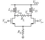
Figure \(\PageIndex{1}\)
What is the CMRR when \(R_{S} = 20\text{ k}\Omega,\: R_{L} = 10\text{ k}\Omega\), the transistor transconductance, \(g_{m} = 50\text{ mS}\), and the drain-source resistance, \(r_{d}\) is \(100\text{ k}\Omega\)?
- Consider the inductively biased differential Class A amplifier shown below. The capacitors can be treated as RF short circuits. \(L_{D}\) is a choke inductor so \(|sL| ≫ R_{L}\). [Parallels Example 3.6.1]
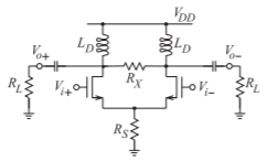
Figure \(\PageIndex{2}\)
- Derive a symbolic expression for the CMRR of the amplifier assuming that the drain-source resistance of the transistors, \(r_{0}\) or \(r_{d}\), is much greater than both \(R_{L}\) and \(R_{X}\), and so can be ignored.
- What is the CMRR when \(R_{S} = 10\text{ k}\Omega,\) \(R_{X} = 30\text{ k}\Omega\), \(R_{L} = 10\text{ k}\Omega\), and the transistor transconductance, \(g_{m}\) is \(10\text{ mS}\).
- Consider the inductively-biased differential Class A amplifier shown below. \(L_{D}\) is a choke inductor so \(|sL| ≫ R_{L}\). [Parallels Example 3.6.1]
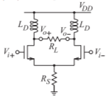
Figure \(\PageIndex{3}\)
- Derive a symbolic expression for the differential mode gain of the amplifier.
- Derive a symbolic expression for the CMRR of the amplifier.
- What is CMRR when \(R_{S} = 10\text{ k}\Omega\), \(R_{L} = 10\text{ k}\Omega\), the transistor transconductance, \(g_{m}\) is \(15\text{ mS}\), and the transistors’ drain-source resistance, \(r_{d}\), is \(100\text{ k}\Omega\)?
- A differential amplifier has a differential-mode gain of \(20\text{ dB}\) and a common-mode gain of \(−3\text{ dB}\).
- What is the the odd-mode gain?
- What is the the even-mode gain?
- Consider the differential amplifier below. [Parallels Example 3.6.1]
Figure \(\PageIndex{4}\)
- What is the differential load impedance?
- What is the odd-mode load impedance?
- What is the common-mode load impedance?
- What is the even-mode load impedance?
- Consider the differential amplifier below. [Parallels Example 3.6.1]
Figure \(\PageIndex{5}\)
- What is the differential load impedance?
- What is the odd-mode load impedance?
- What is the common-mode load impedance?
- What is the even-mode load impedance?
- Consider the differential amplifier below. [Parallels Example 3.6.1]
Figure \(\PageIndex{6}\)
- What is the differential load impedance?
- What is the odd-mode load impedance?
- What is the common-mode load impedance?
- What is the even-mode load impedance?
- If the differential-mode gain of the amplifier is \(20\text{ dB}\) and the common-mode gain is \(2\text{ dB}\), what is the odd-mode gain?
- Consider the differential amplifier below. \(L_{D}\) is a choke inductor so \(|sL| ≫ R_{L}\). [Parallels Example 3.6.1]

Figure \(\PageIndex{7}\)
- What is the differential load impedance?
- What is the odd-mode load impedance?
- What is the common-mode load impedance?
- What is the even-mode load impedance?
- A pseudo-differential amplifier is shown in Figure 3.7.3. Distributed biasing of this amplifier (replacing the inductors and \(R_{DD}\)), presents a common-mode impedance of \(5\:\Omega\) and a differential-mode impedance of \(1\text{ k}\Omega\) to the drain terminals of the transistors in the middle of the amplifier band. The transconductance of each transistor is \(g_{m} = 1\text{ S}\), and the internal parasitics of the transistors can be ignored.
- Draw the common-mode amplifier schematic without the biasing elements. Include the common-mode load resistance \(R_{Lc}\).
- Draw the odd-mode amplifier schematic without the biasing elements. Include the odd-mode load resistance \(R_{Lo}\).
- Draw the even-mode amplifier schematic without the biasing elements. Include the odd-mode load resistance \(R_{Lo}\).
- Draw the differential-mode amplifier schematic without the biasing elements. Include the common-mode load resistance \(R_{Lc}\).
- What is the common-mode gain?
- What is the differential-mode gain?
- What is the common-mode rejection ratio in decibels?
- A pseudo-differential amplifier is shown in Figure 3.7.3. Distributed biasing of this amplifier (replacing the inductors and \(R_{DD}\)), presents a common-mode impedance of \(5\:\Omega\) and an odd-mode impedance of \(1\text{ k}\Omega\) to the drain terminals of the transistors in the middle of the amplifier band. The transconductance of each transistor is \(g_{m} = 100\text{ mS}\) and the internal parasitics of the transistors can be ignored.
- Draw the common-mode amplifier schematic without the biasing elements. Include the common-mode load resistance \(R_{Lc}\).
- Draw the odd-mode amplifier schematic without the biasing elements. Include the odd-mode load resistance \(R_{Lo}\).
- Draw the even-mode amplifier schematic without the biasing elements. Include the odd-mode load resistance \(R_{Lo}\).
- Draw the differential-mode amplifier schematic without the biasing elements. Include the common-mode load resistance \(R_{Lc}\).
- What is the even-mode impedance presented to the amplifier?
- What is the differential-mode impedance presented to the amplifier?
- What is the even-mode voltage gain?
- What is the differential-mode voltage gain?
- What is the common-mode voltage gain?
- What is the odd-mode voltage gain?
- What is the common-mode rejection ratio?
3.11.1 Exercises By Section
\(†\)challenging, \(‡\)very challenging
\(§3.2\: 1†, 2, 3\)
\(§3.5\: 4‡, 5‡, 6†, 7†, 8†, 9†\)
\(§3.6\: 10, 11, 12, 13, 14, 15, 16†, 17†, 18†, 19†, 20, 21, 22, 23†, 24†\)
\(§3.7\: 25†, 26†\)
3.11.2 Answers to Selected Exercises
- (d) \(34.7\:\Omega\)
- (b) \(121\)
- (d) \(1/f^{2}\)
- (c)
\(\begin{array}{l}{8\text{ GHz}, -2.77\text{ dB}}\\{9\text{ GHz}, -0.57\text{ dB}} \\ {10\text{ GHz}, 0\text{ dB}}\\{11\text{ GHz}, -0.33\text{ dB}}\\{12\text{ GHz}, -1.03\text{ dB}}\end{array}\)
- (h) \(-100\)
- (b) \(-3\text{ dB}\)
- \(37.5\:\Omega\)
- (a)

Figure \(\PageIndex{8}\)