
4.6: Case Study- Design of a WiMAX Power Amplifier
- Page ID
- 46071
In this section the design and simulation of a \(10\text{ W}\) power amplifier module using a GaN HEMT transistor, here a Eudyna EGN010MK device, is examined.\(^{1}\) A GaN (gallium nitride) transistor can have a very large drain-source voltage and can produce substantial output power. The amplifier schematic is shown in Figure 4.5.2. The amplifier is targeted for use in a WiMAX data communication system operating from \(3.4\) to \(3.8\text{ GHz}\).
4.6.1 Input and Output Matching Networks
The harmonic balance simulation employed in design uses a large-signal transistor model supplied by the manufacturer of the transistor and, as is usual, it is proprietary and cannot be viewed in the simulator. A
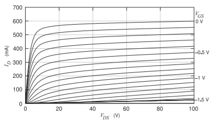
Figure \(\PageIndex{1}\): Output current-voltage characteristics of the active device in the WiMAX amplifier.
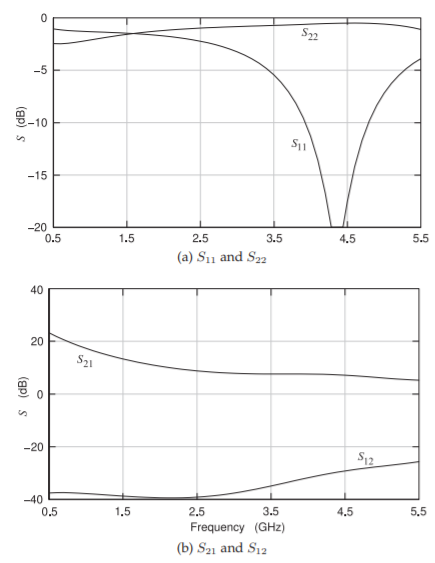
Figure \(\PageIndex{2}\): Small signal scattering parameters of the active device of the WiMAX amplifier.
designer must initially work with the transistor’s output current-voltage characteristic, as shown in Figure \(\PageIndex{1}\). The transistor is biased with a gate-source voltage of \(−1.115\text{ V}\), a drain-source voltage of \(50\text{ V}\), and a drain current of \(100\text{ mA}\). At this bias point the input and output \(50\:\Omega\: S\) parameters of the transistor are as shown in Figure \(\PageIndex{2}\). Examination of \(S_{11}\) in Figure \(\PageIndex{2}\)(a) indicates that the input impedance of the GaN transistor is approximately
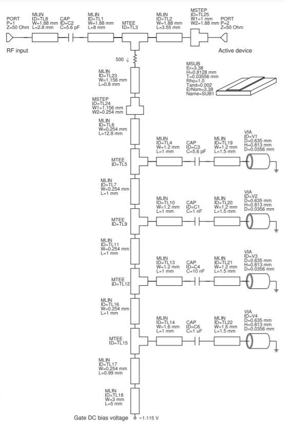
Figure \(\PageIndex{3}\): Input matching network of the WiMAX amplifier.
\(50\:\Omega\) over the WiMAX frequency range of \(3.4–3.8\text{ GHz}\). As a result, very little input matching is required. The circuit model of the input network is shown in Figure \(\PageIndex{3}\). The input network is shown with \(50\:\Omega\) ports at Ports \(1\) and \(2\). These are used in evaluating the \(S\) parameters of the network but are removed when the network is incorporated in the complete amplifier shown
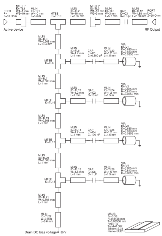
Figure \(\PageIndex{4}\): Output matching network of the WiMAX amplifier.
in Figure 4.5.2.
Examination of the output reflection coefficient of the transistor indicates that it can be approximately modeled by a current source in parallel with a \(33\:\Omega\) resistor and a \(4.4\text{ pF}\) capacitor (an impedance of \(2.5 −\jmath 11\:\Omega\) at \(3.6\text{ GHz}\)) and so output matching is required to transition to \(50\:\Omega\). The circuit model of the output network is shown in Figure \(\PageIndex{4}\). The main component of the output matching network is an approximate one-quarter wavelength long
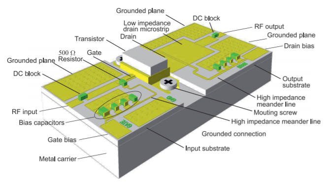
Figure \(\PageIndex{5}\): WiMAX amplifier operating from \(3.4\) to \(3.8\text{ GHz}\).
impedance transformer implemented by the microstrip transmission lines (MLIN) TL1 and TL2. This is the basis of the output network design and other components complete the network.
The complete power amplifier module is shown in Figure \(\PageIndex{5}\). A major consideration in the mechanical assembly is management of the heat produced by the active device. The semiconductor is valence-bonded by the transistor foundry to a metal plate which is secured to the metal carrier using mounting screws and thermal paste between the metal carrier and the metal backing of the transistor. The metal carrier is typically mounted on a heat sink.
The input and output networks are on separate substrates, as this enables the transistor to be mounted directly on the metal carrier. The input substrate supports a microstrip circuit with a \(50\:\Omega\) RF input connected through a DC blocking capacitor to a microstrip line that drives the gate. Near the transistor, the gate microstrip line is connected through a \(500\:\Omega\) resistor to a DC bias network. The \(500\:\Omega\) resistor provides part of the RF isolation between the gate line and the gate bias network. The gate current drawn by the transistor is \(11\:\mu\text{A}\) so that there is a \(0.06\text{ V}\) DC voltage drop across the \(500\:\Omega\) resistor. From the \(500\:\Omega\) isolation resistor, a high-impedance (i.e., narrow) microstrip meander line continues to a sequence of RF shorting capacitors of increasing capacitance ranging from \(5.6\text{ pF}\) next to the meander line to \(1\:\mu\text{F}\) at the gate bias pad from which wirebonds lead to an external source. This arrangement minimizes the impact of the increasing parasitic series inductances of the capacitors as their capacitance values increase. Together, the \(500\:\Omega\) resistor and the high-impedance line provide significant RF isolation from the external bias network. Note that
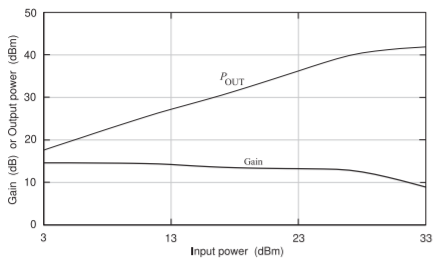
Figure \(\PageIndex{6}\): WiMAX amplifier simulated output power, \(P_{\text{OUT}}\), and gain at \(3.5\text{ GHz}\).
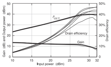
Figure \(\PageIndex{7}\): WiMAX amplifier simulated output power, gain, and drain efficiency at \(3.4,\: 3.5,\: 3.6,\: 3.7,\) and \(3.8\text{ GHz}\).
areas of the input network without microstrip elements are grounded planes. These are regularly shorted by vias to the metal backing of the microstrip substrate, which is in turn connected to the metal carrier. This arrangement suppresses substrate modes.
The output network is similarly arranged, but now the bias resistance is omitted, as the voltage drop across it would be too great since the DC drain bias current is \(100\text{ mA}\). The output impedance of the active device two-port is very low, so the first microstrip line is wide and so has low characteristic impedance. Now RF isolation from the drain bias network is provided by the high-impedance meander line and there is a high-impedance contrast to the low-impedance drain line.
The nonlinear performance of the amplifier is characterized using one-tone and two-tone tests. The one-tone test results are shown in Figure \(\PageIndex{6}\), where the input power of a single input tone, a sinewave, at \(3.5\text{ GHz}\) is swept from \(3\text{ dBm}\) to \(33\text{ dBm}\). The output power at first increases linearly but then begins to saturate and the gain of the device drops. The small-signal gain is \(13.3\text{ dB}\) and the output power at \(1\text{ dB}\) gain compression is \(28.2\text{ dBm}\) while the gain of the amplifier is \(12.3\text{ dB}\). While the gain and output power vary slightly over the WiMAX frequency range of \(3.4\) to \(3.8\text{ GHz}\) (see Figure \(\PageIndex{7}\)), the drain efficiency is more sensitive.
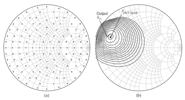
Figure \(\PageIndex{8}\): Simulated output load-pull characterization of the WiMAX amplifier: (a) load-pull points used; and (b) load-pull \(0.1\text{ dB}\) contours of the amplifier at \(3.5\text{ GHz}\) showing the locus of the reflection coefficient looking from the transistor into the output matching network as contours of constant output power. The family of contours begins with the point of maximum output power, \(P_{\text{OUT, MAX}} = 42.6\text{ dBm}\). The output power for the first contour surrounding \(P_{\text{OUT, MAX}}\) is \(42.5\text{ dBm}\) and the powers of the contours then reduce in \(0.5\text{ dB}\) steps. Also shown is the \(S_{11}\) of the final output matching network design from \(3.4\) to \(3.8\text{ GHz}\). The ’Output \(S_{11}\)’ is the reflection coefficient from \(3.4\) to \(3.8\text{ GHz}\) of the output matching network looking from the active device indicating the simulated output power is between \(42.4\text{ dB}\) and \(42.5\text{ dB}\) (approximately). (A complete determination would require load-pull contours at several frequencies.)
4.6.2 Load-Pull
Optimum design of a power amplifier requires load-pull characterization in which, often, the input matching network is already designed, and in simulation a special load-pull element is used for the output matching network. This element can present a range of matching transformations between the output of the active device and the output load. An array of transformations is specified in terms of reflection coefficients such as that shown in Figure \(\PageIndex{8}\)(a). At each of the points, the output power, \(P_{\text{OUT}}\), is calculated and contours of constant output power are interpolated from these data, yielding the load-pull contours shown in Figure \(\PageIndex{8}\)(b). The frequency locus (from \(3.4\) to \(3.8\text{ GHz}\)) of \(S_{11}\) of the output matching network (looking from the active device) is also shown in Figure \(\PageIndex{8}\)(b). The design choice made for the output matching network is for its \(S_{11}\) to be tangential to one of the load-pull contours so that the output power is constant across the frequency band. So rather than designing for maximum power transfer, which practically could only be achieved at one frequency, the design choice is to achieve flat gain across the band. Other quantities can also be plotted in the load-pull test. These include efficiency, the level of harmonics, and distortion terms.
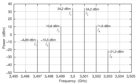
Figure \(\PageIndex{9}\): Simulated output spectrum with a two-tone input signal comprising tones at \(3.500\text{ GHz}\) and \(3.501\text{ GHz}\) each being \(23\text{ dBm}\).
4.6.3 Two-Tone Characterization
The second test used to quantify the nonlinear performance of a power amplifier is the two-tone test in which two closely spaced tones of equal power are applied at the input of the amplifier. The output spectrum is then calculated and tabulated for a range of input powers. The output spectrum under one condition is shown in Figure \(\PageIndex{9}\). The output spectrum consists of amplified versions of the two input tones at \(f_{1} = 3.500\text{ GHz}\) and \(f_{2} = 3.501\text{ GHz}\) as well as intermodulation products separated by multiples of the input tone spacing. The tones at \(f_{3} = 3.499\text{ GHz}\) and \(f_{4} = 3.502\text{ GHz}\) are called third-order intermodulation components, abbreviated as IM3, where \(f_{3} = 2f_{1} − f_{2}\) and \(f_{4} = 2f_{2} − f_{1}\). More specifically, the tone at \(f_{3}\) is called the lower IM3 tone (IM3\(_{\text{L}}\)) and the tone at \(f_{4}\) is called the upper IM3 tone (IM3\(_{\text{U}}\)). The next tones spaced one further interval out, the \(f_{5}\) and \(f_{6}\) tones, are called the fifth-order intermodulation distortion tones, the IM5 tones. Only one of the IM7 tones, \(f_{7}\), has sufficient amplitude to be seen on the scale in the figure. The amplitudes of the output tones are not symmetrical around \(f_{1}\) and \(f_{2}\) and this effect is attributed to the impedance of the baseband circuit, as some of the input signal power is converted to baseband before being converted back up again [39, 40, 41, 42, 43]. The thermal modulation of the transistor characteristics, especially mobility, due to temperature variations at or slower than the rate at which the envelope varies, can also produce this effect. Minimizing temperature variations is an additional reason for very good heat-sinking of power devices.
In Figure \(\PageIndex{10}\) the output power at both the fundamental and IM3\(_{\text{U}}\) are plotted versus the input power in a two-tone test. The output power at the fundamental increases linearly with the input power until saturation is reached. The IM3\(_{\text{U}}\) signal initially increases with the third power of the input signal level, which corresponds to the model of the active device around the bias point at low signal levels being a cubic power series. As the power increases, high-order nonlinearities become significant and the IM3 behavior is less predictable.
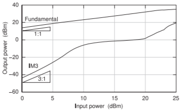
Figure \(\PageIndex{10}\): Response to a two-tone input signal: output power at the fundamental and at IM3\(_{\text{U}}\) versus input power. The two input tones are at \(3.500\text{ GHz}\) and \(3.501\text{ GHz}\) and the fundamental plotted is at \(3.501\text{ GHz}\).
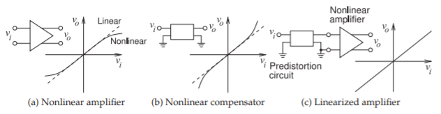
Figure \(\PageIndex{11}\): Predistortion linearizer concept.
4.6.4 Summary
Design of power amplifiers considers discrete tones and in particular uses two tones to characterize distortion. Discrete tones are required in simulation and two-tone characterization is convenient in a laboratory. Of course, digitally modulated signals are not discrete tones, but designers have found that the nonlinear responses to one tone and to two tones are good indications of the behavior with digitally modulated signals which are not convenient to use in simulation [6, 44].
Footnotes
[1]  Design Environment Project File: WiMAX amp.emp.