
4.10: RFIC Power Amplifiers
- Page ID
- 46053
One of the distinguishing features of RFIC design is the synthesis of a circuit that intrinsically has the desired attributes. For an RFIC power amplifier the synthesized circuit must produce low levels of distortion while achieving high efficiency. The fundamental distortion mechanism in an RFIC is the near quadratic \(i-v\) characteristic of a MOS transistor and the tanh-like transfer characteristic of a MOS amplifier. This section has three examples of analytic and circuit techniques for calculating and managing distortion in MOS circuits.
4.10.1 Distortion in a MOSFET Enhancement-Depletion Amplifier Stage
In this section, power series analysis is applied to the MOS enhancement-depletion amplifier stage shown in Figure \(\PageIndex{2}\)(a). This circuit is a Class A amplifier with a common-source enhancement gain stage and a depletion transistor as an active load. Recall that with a MOSFET, the voltage of the substrate has an important effect on operation of the transistor. With enhancement-mode transistors the substrate or body is typically connected
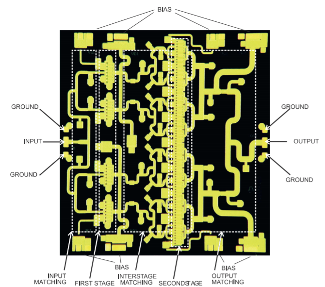
Figure \(\PageIndex{1}\): An \(8–12\text{ GHz}\) MMIC amplifier producing approximately \(1\text{ W}\) of output power with key networks identified. (Courtesy Filtronic, PLC, used with permission.)
to the most negative voltage in the circuit, in this case ground. So, since \(M_{1}\) has the body connected to the source, there is no body effect for \(M_{1}\). However, for \(M_{2}\) the body effect must be considered. Using a simple MOSFET quadratic input-output relationship,
\[\label{eq:1}I_{D1}=\frac{K_{1}}{2}(V_{A}+V_{X}-V_{T0E})^{2}=I_{D2}=\frac{K_{2}}{2}\left(-V_{TD}^{2}\right) \]
where the threshold voltage of \(M_{2}\), with the body effect, is
\[\begin{align}V_{TD}&=V_{T0D}+\gamma\left(\sqrt{2\phi_{F}+V_{B}+V_{Y}}-\sqrt{2\phi_{Y}}\right)\nonumber \\ \label{eq:2}&=V_{1}+\gamma\left(\sqrt{2\phi{F}+V_{B}+V_{Y}}\right)\end{align} \]
(These equations are given in slightly different form in Section 1.A.1. The quantities \(\phi_{F}\) and \(\phi_{Y}\) are built-in inversion potentials.) Also \(K\) is proportional to \(W/L\), where \(W\) is the width of the transistor’s channel and \(L\) is its length. The variable \(V_{1} = V_{T0D} − \gamma\sqrt{2\phi_{Y}}\) has been introduced, but as will be seen it will be canceled during the derivation.
The aim here is to develop a relationship between the input signal \(V_{X}\) and the output signal \(V_{Y}\). The first step in developing a simple relationship that can be used in initial design is to relate the operating point voltage levels. Rearranging Equation \(\eqref{eq:1}\),
\[\label{eq:3}\sqrt{\frac{K_{1}}{K_{2}}}(V_{A}+V_{X}-V_{TOE})=-V_{TD} \]
with the appropriate sign choice made. Combining Equations \(\eqref{eq:1}\) and \(\eqref{eq:2}\) yields
\[\begin{align}\label{eq:4}\sqrt{\frac{K_{1}}{K_{2}}}(V_{A}+V_{X}-V_{TOE})&=-\left(V_{1}+\gamma\sqrt{2\phi_{F}+V_{B}+V_{Y}}\right) \\ \label{eq:5}\text{and }\sqrt{\frac{K_{1}}{K_{2}}}(V_{X})+\sqrt{\frac{K_{1}}{K_{2}}}(V_{A}-V_{TOE})&=-\left(V_{1}+\gamma\sqrt{2\phi_{F}+V_{B}+V_{Y}}\right)\end{align} \]
Now when \(V_{X} =0= V_{Y}\), that is, when there is no AC signal, Equation \(\eqref{eq:5}\) becomes
\[\label{eq:6}\sqrt{\frac{K_{1}}{K_{2}}}(V_{A}-V_{TOE})=-\left(V_{1}+\gamma\sqrt{2\phi_{F}+V_{B}}\right) \]
Substituting Equation \(\eqref{eq:6}\) into Equation \(\eqref{eq:5}\) yields
\[\begin{align}\label{eq:7}\sqrt{\frac{K_{1}}{K_{2}}}V_{X}&=\gamma\sqrt{2\phi_{F}+V_{B}}-\gamma\sqrt{2\phi_{F}+V_{B}+V_{Y}}\\ \label{eq:8}\left(\sqrt{\frac{K_{1}}{K_{2}}}V_{X}-\gamma\sqrt{2\phi_{F}+V_{B}}\right)^{2}&=\gamma^{2}(2\phi_{F}+V_{B}+V_{Y}) \\ \label{eq:9}\frac{K_{1}}{K_{2}}V_{X}^{2}-\left(2\gamma\sqrt{\frac{K_{1}}{K_{2}}}\sqrt{2\phi_{F}+V_{B}}\right)V_{X}+\gamma^{2}(2\phi_{F}+V_{B})&=\gamma^{2}V_{Y}+\gamma^{2}(2\phi_{F}+V_{B})\end{align} \]
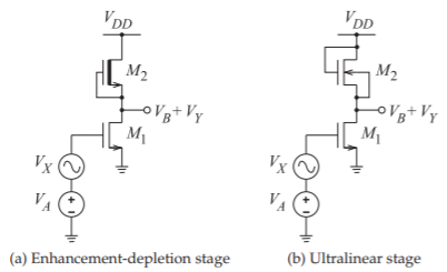
Figure \(\PageIndex{2}\): MOS amplifier stages.
and finally
\[\label{eq:10}\left(\frac{K_{1}}{K_{2}}\right)V_{X}^{2}-\left(2\gamma\sqrt{\frac{K_{1}}{K_{2}}}\sqrt{2\phi_{F}+V_{B}}\right)V_{X}=\gamma^{2}V_{Y} \]
Therefore the component of the output that differs from the quiescent point is
\[\label{eq:11}V_{Y}=\frac{-2}{\gamma}\sqrt{\frac{K_{1}}{K_{2}}}\sqrt{2\phi_{F}+V_{B}}V_{X}+\frac{1}{\gamma^{2}}\frac{K_{1}}{K_{2}}V_{X}^{2} \]
For a sinusoidal input \(V_{X} = |V_{X}| \cos(\omega t)\), \(V_{X}^{2} =\frac{1}{2}|V_{X}|^{2} +\frac{1}{2} |V_{X}|^{2} \cos(2\omega t)\), which contains the second harmonic of the input signal.
So the second-harmonic distortion level, HD\(_{2}\), the ratio of the second-harmonic component of \(V_{Y}\) to the fundamental component, is
\[\begin{align}\text{HD}_{2}&=\left(\left|\frac{1}{2}\frac{K_{1}}{K_{2}}\frac{1}{\gamma^{2}}V_{X}^{2}\right|\right)\left(\left|\frac{-2\sqrt{2\phi_{F}+V_{B}}}{\gamma}\sqrt{\frac{K_{1}}{K_{2}}}V_{X}\right|\right)^{-1}\nonumber \\ \label{eq:12}&=\frac{1}{4\gamma\sqrt{2\phi_{F}+V_{B}}}\sqrt{\frac{K_{1}}{K_{2}}}|V_{X}|\end{align} \]
Examination of Equations \(\eqref{eq:11}\) and \(\eqref{eq:12}\) leads to the following conclusions. If there is a lot of voltage gain (\(∝\sqrt{K_{1}/K_{2}}\)), then the input signal level must be small to keep the harmonic distortion down. Other design considerations that have the same effect are to use a wider device, which increases the transconductance (since \(g_{m}\approx K ∝ W/L\)) of the transistor so that the drain current will be maintained for the lower input voltage levels. Of course, making the device wider increases capacitive parasitics, which will reduce the maximum operating frequency. Making the channel of the device shorter also increases the transconductance while not affecting the frequency performance. The important point is that there are trade-offs in modifying the performance of the circuit and these are only made apparent using the type of analysis presented here. The use of analysis and the optimization of design through synthesis is one of the cornerstones of RFIC design. In large part this is possible because of the (soft) quadratic-like current-voltage characteristics of MOSFETs.
4.10.2 Distortion in the Ultralinear MOS Connection
The circuit in Figure \(\PageIndex{2}\)(b) is an enhancement-mode gain stage with an enhancement-mode load. Transistor \(M_{2}\) is the n-channel enhancement load with its well tied to its source. That is, in the fabrication of \(M_{2}\), a well is formed and the transistor is constructed in the well. The well now serves as the substrate for \(M_{2}\). Since the well and the source of \(M_{2}\) are connected together, \(M_{2}\) is not subject to the body effect. One important property of this circuit is that the characteristics of \(M_{1}\) and \(M_{2}\) are matched. Using a similar approach to that used in the previous section, the input/output relationship of the circuit can be developed. Equating drain currents,
\[\label{eq:13}I_{D1}=\frac{K_{1}}{2}(V_{A}+V_{X}-V_{T0E})^{2}=I_{D2}=\frac{K_{2}}{2}(V_{DD}-V_{B}-V_{Y}-V_{T0E})^{2} \]
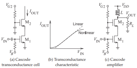
Figure \(\PageIndex{3}\): A MOS cascode amplifier. \(L\) is a choke inductor and is an RF open circuit. \(V_{B}\) and \(V_{G2}\) are bias voltages. The cascode transconductance cell is used in this section as a tanh cascode cell (TCC).
With
\[\label{eq:14}V_{X}=V_{Y}=0,\qquad\sqrt{\frac{K_{1}}{K_{2}}}(V_{A}-V_{T0E})=V_{DD}-V_{B}-V_{T0E} \]
Therefore
\[\label{eq:15}\sqrt{\frac{K_{1}}{K_{2}}}V_{X}+(V_{DD}-V_{B}-V_{T0E})=(V_{DD}-V_{B}-V_{Y}-V_{T0E}) \]
and so
\[\label{eq:16}V_{Y}=-\sqrt{\frac{K_{1}}{K_{2}}}V_{X} \]
The result is that, provided the transistors are matched, the amplifier is inherently linear. So within the approximations of the drain current expressions there is no distortion, and this includes no third-order intermodulation distortion or spectral regrowth.
4.10.3 RFIC Power Amplifiers with Minimal Distortion
The most widely used linear-by-design strategy for linear RFIC amplifier design is to use what is called the multi-tanh method [66]. The idea is to scale several parallel amplifier stages to obtain an overall linear characteristic. Consider the MOS cascode amplifier shown in Figure \(\PageIndex{3}\)(c), which is based on the transconductance cell shown in Figure \(\PageIndex{3}\)(a). Applying an input voltage, \(V_{\text{IN}}\), produces an output current, \(I_{\text{OUT}}\), with the tanh-like characteristic shown in Figure \(\PageIndex{3}\)(b). This characteristic is the dominant cause of amplitude distortion in a FET amplifier. The design strategy for linearizing the output characteristic of a FET amplifier is to put multiple amplifier stages in parallel so that the overall current-voltage characteristic optimally combines the tanh-like characteristic of each stage.
Figure \(\PageIndex{4}\) shows two circuits that exploit the multi-tanh strategy. Figure \(\PageIndex{4}\)(a) is a three-stage multi-tanh differential amplifier transconductance cell in which the bias currents \(I_{B1},\: I_{B2},\) and \(I_{B3}\) are adjusted so that the overall input-output characteristic, \(I_{\text{OUT}}\) versus \(V_{\text{IN}}\), has greater linearity than that of the individual stages [66]. A similar concept is used to combine the output of multiple cascode stages (see Figure \(\PageIndex{4}\)(b)) and this is a topology more suited to the development of RFIC power amplifiers [67].
As an example of the use of the multi-tanh design approach, consider the multiple tanh cascode amplifier in Figure \(\PageIndex{4}\)(b) with three tanh cascode cells (TCCs). This amplifier has both amplitude and phase distortion. The amplitude distortion largely results from the tanh-like current-voltage
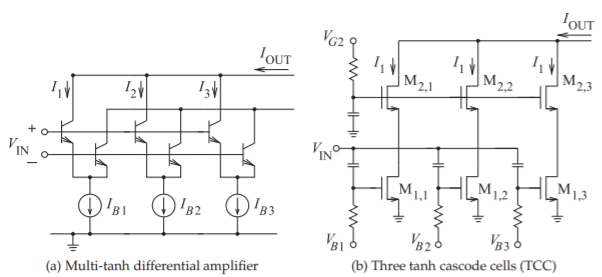
Figure \(\PageIndex{4}\): Combining the output from multiple stages to obtain a highly linear overall transconductance characteristic.
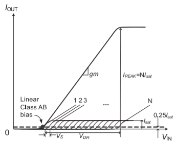
Figure \(\PageIndex{5}\): Combining the output from \(N\) Class AB cascode stages to obtain a highly linear overall transconductance characteristic. Shown are the individual \(I_{\text{OUT}}\) versus \(V_{\text{IN}}\) characteristics of each of \(N\) transistors each biased differently. The combined \(I_{\text{OUT}}\) versus \(V_{\text{IN}}\) characteristic is the sum of the individual transistor’s \(I_{\text{OUT}}\) After [67].
characteristic of the individual cascode stages. Phase distortion largely results from the nonlinearity of the gate capacitance of the FETs. The tanh characteristic of each tanh cascode cell in Figure \(\PageIndex{4}\)(b) is adjusted by scaling the transistors \(M_{1,1},\: M_{1,2},\) and \(M_{1,3}\), and changing their bias voltages \(V_{B1},\: V_{B2},\) and \(V_{B3}\). The design approach is illustrated in Figure \(\PageIndex{5}\) and a synthesis approach is presented in references [68] and [67]. Each tanh cascode stage operates in high Class AB mode and with appropriate biasing the tanh characteristics are staggered. Note that for small input signals only one or a few stages are active. The currents from each stage are summed to yield an overall linearized transconductance response.
Phase distortion is reduced by using an analog predistortion circuit that realizes a nonlinear capacitance network that cancels the combined nonlinear gate capacitance of the cascode stages. The complete CMOS RF power amplifier topology is shown in Figure \(\PageIndex{6}\), where NCN is the nonlinear capacitor network. The die micrograph of this amplifier is shown in Figure
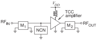
Figure \(\PageIndex{6}\): Complete RFIC power amplifier with a TCC amplifier with 12 Class AB TCC cells and a nonlinear capacitor network (NCN) and input and output matching networks (\(\text{M}_{1}\) and \(\text{M}_{2}\)). After [67].
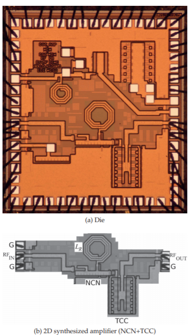
Figure \(\PageIndex{7}\): Die micrograph of the 2D synthesized amplifier with tanh cascode cell (TCC) amplifier stage and nonlinear capacitor network (NCN) stage. (There are two operating at different frequencies, one at the top of the die and one at the bottom. The bottom one is being referred to here.) The die also contains a TCC amplifier, an NCN network, and a conventional RF CMOS Class AB amplifier. The supply is \(3.6\text{ V}\) and the ground connection is identified by \(\mathsf{G}\). The die is shown in (a) and the 2D synthesized amplifier in (b). The inductor \(L_{R}\) resonates out the linear component of the NCN capacitance and the linear component of the gate capacitance of the TCC amplifier. The matching networks and the coke inductor from \(V_{DD}\) are off-chip.
\(\PageIndex{7}\)(a) together with test circuits. The TCC amplifier with the nonlinear capacitor network is broken out in Figure \(\PageIndex{7}\)(b). The performance of the RFIC power amplifier has excellent performance, as shown in Figure \(\PageIndex{8}\), and achieves an output power of \(25\text{ dBm}\) with an efficiency of \(42\%\) and an ACPR of \(−22\text{ dBc}\).
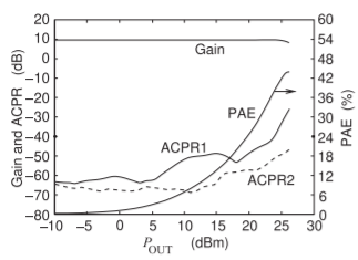
Figure \(\PageIndex{8}\): Performance of the TCC amplifier with the nonlinear capacitor predistortion circuit at \(960\text{ MHz}\) with a WCDMA test signal. A gain of \(9.4\text{ dB}\) with power-added efficiency of \(41.6\%\) is achieved with an output power of \(24.9\text{ dBm}\) and meeting the 3G ACPR1 specifications of \(−33\text{ dBc}\) and an ACPR2 of \(−43\text{ dBc}\). After [67].