
5.4: Case Study- Reflection Oscillator
- Page ID
- 46090
In this case study\(^{1}\) the design of the reflection oscillator shown in Figure \(\PageIndex{1}\)(a) is examined. This is an \(18\text{ GHz}\) common-gate oscillator with series inductive feedback provided by the transmission line TL\(_{1}\). This circuit is derived from the Colpitts oscillator configuration. The resonator is resonant considerably below the oscillation frequency, and so presents a capacitance to the source of the transistor at the oscillation frequency.
5.4.1 Design Procedure
The circuit in Figure \(\PageIndex{1}\)(a) is a modified common-base Colpitts oscillator and the RF equivalent circuit required to understand oscillator operation, and how the circuit corresponds to the standard Colpitts oscillator, are shown in Figure \(\PageIndex{2}\). This is the most common fixed-frequency microwave oscillator topology.
The Colpitts feedback network is shown in Figure \(\PageIndex{2}\)(a) where an inductor provides feedback from the output to the input of the active device. Returning to the modified Colpitts oscillator of Figure \(\PageIndex{1}\), \(L_{1}\) is a large choke inductor presenting an RF open circuit and \(C_{1}\) is a large DC blocking capacitor presenting an RF short circuit. The gate transmission line, TL\(_{1}\), presents a small inductance and most importantly provides inductive feedback from the output to the input of the active device and closely corresponds to \(L_{3}\) in the Colpitts feedback network of Figure \(\PageIndex{2}\)(a). The gate-source and drain-source parasitic capacitances of the transistor, \(C_{GS}\) and \(C_{DS}\), correspond approximately to capacitors \(C_{1}\) and \(C_{2}\) in the Colpitts feedback network. This results in the RF equivalent circuit shown in Figure \(\PageIndex{2}\)(b). In Figure \(\PageIndex{2}\)(b) \(X_{R}\) is the reactance of the resonator and compensates for the nonideal nature of the modified Colpitts oscillator. Stable operation of this oscillator requires that \(X_{R}\) be capacitive but have a variation with frequency substantially less than that of a capacitor. This is accomplished by having the oscillation frequency above the resonant frequency of the resonator.
In Figure \(\PageIndex{1}\) the reflection oscillator is composed of two networks, the active device network and the resonator network. The third network shown, the OscProbe network, is a probe used to control oscillator analysis using the harmonic balance method. The design approach here is to develop a topology incorporating the active device that presents a negative resistance at the interface, \(\mathsf{X}\), between the active device network and the resonator network. Since the active device and the resonator are each best modeled as parallel circuits, it is best to refer to admittance and so the active device network presents a negative conductance to the resonator. In addition, the small-signal admittances of the active network, \(Y_{d} = G_{d} +\jmath B_{d}\), and of the resonator network, \(Y_{r} = G_{r} + \jmath B_{r}\), are shown in Figure \(\PageIndex{3}\). Here the active network has a small-signal conductance that is negative and a small-signal
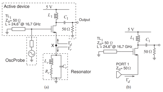
Figure \(\PageIndex{1}\): Reflection oscillator: (a) complete oscillator circuit used in simulation; and (b) configuration for measuring the large-signal reflection coefficient of the active device. \(L_{r} = 5.6\text{ nH}\), \(R_{r} = 10\:\Omega\), \(C_{r} = 445\text{ fF}\), \(L_{1} = 15\text{ nH}\), and \(C_{1} = 10\text{ pF}\). The resonant frequency of the resonator is \(3.19\text{ GHz}\), but this is not the oscillation frequency. It presents the required slope of susceptance with respect to frequency at the oscillator frequency of \(17.76\text{ GHz}\).
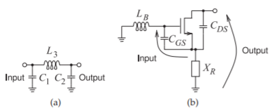
Figure \(\PageIndex{2}\): Operation of the modified Colpitts oscillator: (a) Colpitts feedback network; (b) the essential RF equivalent circuit of the Modified Colpitts oscillator of Figure \(\PageIndex{1}\).
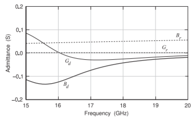
Figure \(\PageIndex{3}\): Small-signal admittance of the active device, \(Y_{d} = G_{d}+\jmath B_{d}\), and admittance of the resonator, \(Y_{r} = G_{r} + \jmath B_{r}\). \(B_{d}\) varies with frequency largely because of the frequency-dependent feedback provided by TL\(_{1}\).
susceptance that is inductive. The resonator has negligible conductance and a capacitive susceptance.
The admittance looking into the source of the active network depends on the level of the signal at \(\mathsf{X}\) in Figure \(\PageIndex{1}\). However, the admittance of the resonator is independent of the signal level since the resonator is a linear network. The design strategy is then to develop a feedback network, here the transmission line, TL\(_{1}\), in the gate of the FET, that then presents a negative conductance to a frequency-selective structure, the resonator network.
The effect of the signal level is examined using the active network test circuit shown in Figure \(\PageIndex{1}\)(b). Here a \(50\:\Omega\) generator, at Port \(\mathsf{1}\), drives the source of the active device. The power of the signal at the port is varied and it is found that the negative conductance varies from \(−0.0274\text{ S}\) at a small applied signal, to \(−0.0224\text{ S}\) at an applied signal level of \(−10\text{ dBm}\), to \(−0.004\text{ S}\) at \(−7\text{ dBm}\), and to \(0.001\text{ S}\) at \(−6\text{ dBm}\). Oscillation will occur when the conductance looking into the source terminal of the active device is approximately zero (since the conductance of the resonator is negligible) and the susceptances of the active network and the resonator network cancel.
Unfortunately the susceptance of the active network changes as the signal level varies since the active device capacitances are nonlinear. The effect of this will now be examined. It is instructive to view the effect of signal level on the oscillation condition by considering the reflection coefficients \(\Gamma_{d}\) for the active device network and \(\Gamma_{r}\) for the resonator network. This is shown in Figure \(\PageIndex{4}\), where a polar plot is used since \(|\Gamma_{d}| > 1\) (except for a very large signal at \(\mathsf{X}\)). \(\Gamma_{r}\) is approximately on the unit circle and is capacitive being in the lower half plane. \(\Gamma_{d}\) is shown for several signal levels, with a signal level of \(−20\text{ dBm}\) corresponding to the small-signal condition. As the signal level increases eventually to \(−6\text{ dBm}\), both the conductance and susceptance of the active device change. The device conductance becomes positive as \(\Gamma_{d}\) crosses inside the unit circle. Resonance occurs when \(\Gamma_{d}\Gamma_{r} = 1\). Since \(G_{r} \approx 0\), this is when \(\Gamma_{d}\approx 1/\Gamma_{r}\). That is, resonance will occur at the frequency where the locus of \(\Gamma_{d}\) intersects with \(1/\Gamma_{r}\).
The results presented in Figure \(\PageIndex{4}\) for the reflection coefficient of the active network in Figure \(\PageIndex{1}\)(b) are derived from a large-signal solution calculated using harmonic balance analysis. In most harmonic balance analyses it is only necessary to consider a few harmonics to obtain good results. In the simulation here, five harmonics are considered, with the fundamental frequency set by the frequency of the source at the driven port. The fundamental frequency was stepped from \(15\text{ GHz}\) to \(20\text{ GHz}\). Oscillator
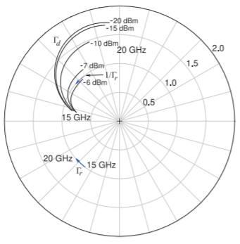
Figure \(\PageIndex{4}\): Reflection coefficient of the resonator, \(\Gamma_{r}\), and of the active device, \(\Gamma_{d}\), at various signal levels. \(\Gamma\) is plotted on a polar plot with the outer circle corresponding to \(|\Gamma| = 2\). As desired, the locus of \(1/\Gamma_{r}\) is parallel to \(\Gamma_{d}\) at a fixed signal level (here about \(−6\text{ dB}\)), and the direction of \(1/\Gamma_{r}\) with increasing frequency is opposite that of \(\Gamma_{d}\). The close parallel match is ensured by adjusting the susceptance-versus-frequency slope of the resonator. Considering the intersection of \(1/\Gamma_{r}\) and \(\Gamma_{d}\) is equivalent to considering the intersection of \(1/\Gamma_{d}\) and \(\Gamma_{r}\).
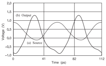
Figure \(\PageIndex{5}\): Voltage waveforms at the output of the oscillator (Curve (b)), and at the source terminal of the active device, Terminal \(\mathsf{x}\), which is the interface between the active device and the resonator (Curve (a)).
simulation also uses harmonic balance analysis, but now the frequency of oscillation is not known ahead of time. It is necessary to introduce another condition to enable the simulator to find the oscillation frequency. One of the techniques used in harmonic balance simulators is the introduction of an oscillator probe element such as the \(\mathsf{OscProbe}\) element shown in Figure \(\PageIndex{1}\)(a). The frequency of the source, \(F_{\text{OSC}}\), in the \(\mathsf{OscProbe}\) element is initially guessed by the simulator and the series impedance of the \(\mathsf{OscProbe}\) element is a short circuit at the oscillation frequency and an open circuit at the harmonics. This extra condition is included in the harmonic balance equations and \(F_{\text{OSC}}\) is allowed to vary as well as the amplitude of the source. The oscillation solution is obtained when the current through the impedance in the \(\mathsf{OscProbe}\) element is zero. The oscillation frequency is found to be \(17.76\text{ GHz}\). Note that this is not the resonant frequency of the resonator, as here the active device presents an inductance to the resonator. The resonator must present an effective capacitance that has the required susceptance-versus-frequency slope so that the frequency locus of \(1/\Gamma_{r} (f)\) is parallel but oppositely directed to that of \(\Gamma_{d} (f)\) (see Figure \(\PageIndex{4}\)).
Figure \(\PageIndex{5}\) shows the waveforms at the output of the oscillator (Curve (b)) and at the interface (\(\mathsf{X}\)) between the resonator and active device networks
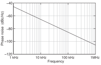
Figure \(\PageIndex{6}\): Phase noise of the reflection oscillator.
(Curve (a)). The output of the oscillator would be followed by a bandpass filter so that a single harmonic-free sinewave is presented to the external output terminal.
The phase noise of the oscillator is calculated from the oscillator steadystate conditions and is shown in Figure \(\PageIndex{6}\). The phase noise level is relatively high and this is principally due to the resistance \(R_{r}\) in the resonator, which models the loss in the lumped inductor. Performance would be improved if, instead, a distributed circuit (with transmission lines) was used to realize the required admittance and its derivative at the oscillation frequency.
5.4.2 Summary
The zero combined suspectance point in Figure \(\PageIndex{3}\) was at \(17.76\text{ GHz}\) while the oscillation frequency shown in Figure \(\PageIndex{5}\) is at \(17.29\text{ GHz}\). The reason for this discrepancy is that the susceptance plot in Figure \(\PageIndex{3}\) is based on small-signal conditions whereas the simulation is for a large signal and includes harmonics. It can be expected that the oscillation frequency calculated using harmonic balance analysis will be different from that obtained from a small-signal analysis. Consider the \(\Gamma_{d}\) curves in Figure \(\PageIndex{4}\). (Generating this data took many simulation runs and did not consider harmonics.) The magnitude of \(\Gamma_{d}\) reduces as the applied signal level increases. This rotation is not desired and means that the susceptance of the active device is amplitude-dependent. This corresponds to the magnitude of the negative conductance of the active device getting smaller. Note that there is also a small rotation of \(\Gamma_{d}\) indicating that the susceptance of the active device also changes as the signal level increases. This means that the oscillation frequency will depend on the amplitude of the oscillation. In addition, the applied signal used to calculate the \(\Gamma_{d}\) at different power levels is not the actual oscillating signal.
Footnotes
[1]  Design Environment Project File: Reflection_Oscillator.emp.