
5.5: Voltage-Controlled Oscillator (VCO)
- Page ID
- 46091
This section describes the special challenges in designing a microwave VCO. The main challenge derives from the resonator network now being lossy because of the use of a tuning element that unfortunately has low \(Q\). In nearly all cases the tuning element is a varactor, a reverse-biased pn-junction or Schottky diode, which has substantial series resistance at microwave frequencies. This means that the full Kurokawa conditions for stable oscillation must be used and also these conditions must be met across the tuning range of the oscillator and during start-up.
5.5.1 Design Procedure
A broadband VCO is a key element in a communication system and is commonly used to drive a mixer to enable different frequency bands to be selected simply by changing the oscillation frequency. The design of a broadband VCO is relatively complex, with issues of simultaneous oscillation at multiple frequencies, phase noise, and power efficiency being of primary concern. In a battery-powered communication device the power drawn by the VCO is a substantial fraction of the total power consumed by the RF front end.
The design of a VCO builds on the standard oscillator design procedure which matches the inverse reflection coefficient of the active device, \(1/\Gamma_{d}\), to the reflection coefficient of a tank or resonator circuit, \(\Gamma_{r}\), so that \(\Gamma_{r} = 1/\Gamma_{d}\) only at oscillation. This is complicated at microwave frequencies as parasitic capacitances are significant and special design strategies are required to mitigate their effect. The required stable oscillation conditions must be achieved over the entire tuning range while also maintaining constant output power and low phase noise.
Two VCO circuits are shown in Figure \(\PageIndex{1}\). The circuit in Figure \(\PageIndex{1}\)(a) is a common-base oscillator with the feedback provided by the base inductor, \(L_{B}\), presenting a negative conductance and a small shunt inductance at the emitter. The resonant circuit comprising \(C_{R}\) and \(L_{R}\) presents either a capacitance or an inductance at the oscillation frequency, and cancels the susceptance presented by the active device. The resonant circuit has a non-negligible conductance due to loss in the resonator. Ideally the active device’s susceptance is independent of amplitude, however, the transistor’s parasitics complicate the situation so that this susceptance also has amplitude dependence. The resonator is tunable because of the variable
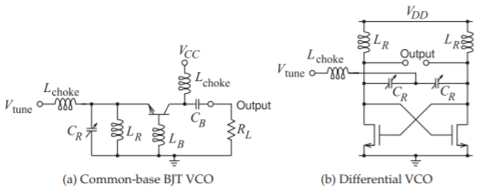
Figure \(\PageIndex{1}\): VCO with tunable resonator comprising \(C_{R}\) and \(L_{R}\). \(L_{\text{choke}}\) is an RF open circuit and \(C_{B}\) is an RF short circuit.
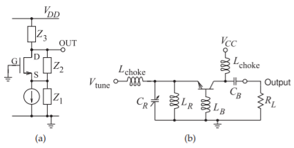
Figure \(\PageIndex{2}\): Common-gate/base feedback oscillator using a Pi-type feedback networks: (a) common-gate FET oscillator; and (b) common-base BJT oscillator.
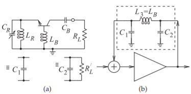
Figure \(\PageIndex{3}\): Transformation of the oscillator of Figure \(\PageIndex{2}\) into the form of a standard Colpitts feedback oscillator: (a) first stage of transformation replacing the \(L_{\text{choke}}\)s with RF open circuits, replacing \(C_{B}\) with an \(R_{F}\) short circuit; and (b) final feedback form (compare with the circuits in Figures 5.2.2(a) and 5.2.3(b)). \(C_{1}\) combines the inductance of the \(L_{r}-C_{r}\) resonator and the capacitive susceptance introduced by the device parasitics. \(C_{2}\) derives mostly from the collector-emitter capacitance.
capacitance, usually a varactor.
The most common microwave single-transistor reflection oscillator topology is the common-base Colpitts BJT/HBT oscillator, or the similar common-gate FET oscillator, as shown in Figure \(\PageIndex{2}\). Consider the BJT oscillator in Figure \(\PageIndex{2}\)(b). This is called a common-base configuration, although it is only approximate as will be seen when the RF signal flow path is traced. The parallel \(L_{R}-C_{R}\) combination is called a resonator, but it is resonant below (or above) the oscillation frequency, so at the oscillation frequency it is effectively a capacitor (or an inductor) but with an admittance-versus-frequency slope magnitude that is less than that of a lumped capacitor (or inductor).\(^{1}\) Design of the susceptance slope is important to obtaining successful operation as a VCO. Thus one of the purposes of \(L_{R}\) is to enable \(\partial B_{r}/\partial\omega\) to be selected in design. The base inductance \(L_{B}\) couples the output of the active device at the collector to the input at the emitter. So this circuit is a common-base Colpitt’s oscillator (the equivalence is illustrated in Figure \(\PageIndex{3}\)).
Parasitic and design elements (especially \(L_{B}\) and compensating capacitors) in the active network may require that the resonant network present an inductance. As long as the Kurokawa condition is met oscillation will be stable. VCO design requires considerable flexibility.
Figure \(\PageIndex{1}\)(b) is the schematic of a differential oscillator realized using MOSFETs, where the resonator comprises a pair of variable capacitances, the \(C_{R}\)s, and a pair of inductors, the \(L_{R}\)s. The chokes, the \(L_{\text{choke}}\)s, are short circuits at DC but block RF currents. On-chip design has many restrictions and it cannot be expected that the same performance can be obtained as with a hybrid design.
5.5.2 Managing Multioscillation and Phase Noise
The oscillation condition for a stable reflection oscillator needs to be revisited and discussed with respect to a VCO. Referring to the reflection oscillator in Figure 5.3.1, the Kurokawa oscillator condition for stable (single-frequency) oscillation is [11]
\[\label{eq:1}\left.\left(\frac{\partial G_{d}}{\partial V}\frac{\partial B_{r}}{\partial\omega_{0}}-\frac{\partial B_{d}}{\partial V}\frac{\partial G_{r}}{\partial\omega_{0}}\right)\right|_{V=V_{0},\omega=\omega_{0}}>0 \]
where the the subscript \(0\) refers to the operating point and \(V_{0}\) is the amplitude of the oscillation at the interface of the active and resonator networks. The active network includes elements added to the active device mainly to compensate for parasitics. If the condition in Equation \(\eqref{eq:1}\) is not met, then the oscillator may simultaneously oscillate at multiple frequencies or be chaotic.
Achieving single-frequency oscillation can be a challenge for fixedfrequency oscillator design but is especially challenging for a VCO as the condition must be met across the tuning range. Complicating design further is that with a VCO the resonator network is lossy so that the Kurokawa condition is not simplified as it is for a fixed-frequency oscillator, see Section 5.3.1. The condition is simplified then because of of the high \(Q\) resonator of a fixed-frequency oscillator where terms in Kurokawa’s oscillation condition disappear because \(G_{r}\approx 0\).
In VCO design the design procedure must be kept simple, and this opens up the design space to enable optimization of other characteristics such as minimizing phase noise and DC power consumption. One aspect of the preferred oscillator design procedure is to choose a topology that results in an effective device susceptance that as much as possible is independent of signal amplitude (i.e., \(\partial B_{d}/\partial V |_{V =V_{0}}\approx 0\)) and a loaded resonator conductance that is independent of frequency (i.e., \(\partial G_{r}/\partial\omega_{0}|_{\omega=\omega_{0}}\approx 0\)). Then the criterion for stable oscillation is the much simpler
\[\label{eq:2}\left.\left(\frac{\partial G_{d}}{\partial V}\right)\left(\frac{\partial B_{r}}{\partial\omega_{0}}\right)\right|_{V=V_{0},\omega=\omega_{0}}>0 \]
something that is much easier to satisfy in design. This equation is the same as the simplified criteria developed for the fixed-frequency oscillator but now there are two additional design requirements, i.e. \(\partial B_{d}/\partial V |_{V =V_{0}}\approx 0\) and \(\partial G_{r}/\partial\omega |_{\omega =\omega_{0}}\approx 0\).
Referring to the common-base circuit of Figure \(\PageIndex{3}\)(a), the element in the base, \(L_{B}\), induces a negative conductance at the interface with the \(L_{R}-C_{R}\) resonator [18]. It also induces an inductive susceptance and with the active device capacitance and other capacitors the total susceptance presented by the active network is either inductive or capacitive. A feature of the circuit in Figure \(\PageIndex{3}\)(a) is that the \(L_{R}-C_{R}\) resonator is isolated from the load
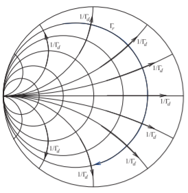
Figure \(\PageIndex{4}\): Requirements on \(\Gamma_{r}\) and \(\Gamma_{d}\) for stable oscillation as derived from Equation \(\eqref{eq:2}\) with assumptions behind the derivation of the equation (i.e., \(\partial B_{d}/\partial V|_{V =V_{0}}\approx 0\) and \(\partial G_{r}/\partial\omega_{0}|_{\omega =\omega_{0}}\approx 0\)). The locus of \(\Gamma_{r}\) is for increasing frequency. Several loci are shown for \(1/\Gamma_{d}\) are shown at different frequencies. The arrowed loci of \(1/\Gamma_{d}\) are for increasing frequency.
and so the load has little effect on the oscillation frequency. The output of the transistor is modeled as a shunt connection of a current source, a conductance, and a susceptance. Thus it is natural to treat the oscillator as a negative conductance oscillator. It is found that, as desired, this topology leads to a negative conductance that reduces in magnitude as the oscillation level increases. Another way of stating the same issue is saying that the \(L_{r}-C_{r}\) resonator network does not contain all of the reactance that should be assigned to \(C_{1}\) in the simple Colpitts oscillator. Now \(\partial G_{d}/\partial V|_{V =V_{0}}\) in Equation \(\eqref{eq:2}\) is positive. (That is, \(G_{d}\) becomes less negative as the magnitude of the oscillating signal increases.) Thus for stable oscillation, \(\partial B_{r}/\partial\omega |_{\omega =\omega_{0}}\) must be positive. The conditions for stable oscillation, using the design simplifications that led to Equation \(\eqref{eq:2}\), are then as shown in Figure \(\PageIndex{4}\). What this figure indicates is that if \(\Gamma_{d}\) is capacitive (\(1/\Gamma_{d}\) is in the top half plane) then \(\Gamma_{r}\) needs to be inductive, while if \(\Gamma_{d}\) is inductive (\(1/\Gamma_{d}\) is in the bottom half plane) then \(\Gamma_{r}\) needs to be capacitive.
At microwave frequencies, parasitic reactances of a transistor are significant and so the active device does not have a signal-level independent susceptance (i.e., \(\partial B_{d}/\partial V|_{V =V_{0}}\) is finite). In part this is because the parasitic capacitances of the transistor are voltage dependent. It is also due to the reactive feedback element used to produce the negative conductance. Parasitic elements further isolate the negative output conductance of a transistor from the port of the active network that interfaces with the resonator. As a result it may be necessary to introduce compensatory elements to translate the behavior of the active device into the correct form. This will be presented in the case study of the next section. The bottom line is that designing for \(\partial B_{d}/\partial V|_{V =V_{0}}\approx 0\) is a major challenge. It is a less significant a problem to design the resonator to have the required conductance property (i.e., \(\partial G_{r}/\partial\omega |_{\omega =\omega_{0}}\approx 0\)).
5.5.3 Negative Resistance Oscillator
The above discussion concerns a negative conductance oscillator in which the magnitude of the device’s negative conductance reduces with signal amplitude. Alternatively, a negative resistance oscillator could be realized using a capacitor in series with the emitter. This leads to an oscillator model in which the negative resistance is in series with a load resistance and a series resonant circuit. Stable oscillation of this oscillator requires that the magnitude of the negative resistance reduce as the oscillation signal increases in size. However, it is difficult to realize a negative resistance that reduces in magnitude as the signal level increases and simultaneously achieve a reactance that is unchanged by the signal level. Thus it is better to use feedback to create a negative conductance shunting a susceptance. Design of a stable negative resistance oscillator is quite difficult and is nearly always avoided.
5.5.4 Summary
With the low \(Q\) resonator of a VCO the design procedure is quite different to that for a fixed-frequency oscillator which has a high \(Q\) resonator. The central reflection-based VCO design concept is the development of an active network presenting a near-voltage-independent susceptance (i.e., \(\partial B_{d}/\partial V|_{V =V_{o}}\approx 0\)) and a frequency-independent negative conductance (\(\partial G_{d}/\partial\omega |_{\omega =\omega_{0}}\approx 0\)). Once this is achieved, the conventional reflection oscillator design approach can be used and the resonator designed so that \(\partial G_{r}/\partial\omega |_{\omega =\omega_{0}}\approx 0\). Design is both an art and a science. Sometimes the problem must be simplified for the designer to be able to conceptualize and synthesize the required circuit. This is usually the best approach to achieving microwave circuits that have near optimum performance. Simply optimizing a given topology is not enough. The correct topology must be synthesized first.
The requirements for oscillation start-up have not been considered yet, and these will be addressed in the following VCO design case study.
Footnotes
[1] The base inductor \(L_{B}\) can be adjusted so that either a capacitive or inductive susceptance is presented to the resonator. As will be seen stable oscillation can be achieved either way.