
5.6: Case Study- Design of a C-Band VCO
- Page ID
- 46094
This section presents the design of a high-performance microwave VCO operating from \(4.5\) to \(5.3\text{ GHz}\) reported in [19]. The design objective is the generation of a frequency-independent negative conductance, \(G_{d}(A)\), with a prescribed reflection coefficient shape, \(\Gamma_{d}\), using a three-terminal active device in a common-base configuration with series-inductive feedback. The oscillator schematic is shown in Figure \(\PageIndex{1}\)(a). This is a common-base oscillator in which the \(2.2\text{ nH}\) base inductor \(L_{3}\) provides negative feedback between the input and output of the transistor and the resonator presents an inductance at the oscillation frequency. So this circuit is a common-base Colpitts oscillator; the equivalence is illustrated in Figure \(\PageIndex{2}\).
5.6.1 Design Philosophy and Topology
Referring to Figure \(\PageIndex{1}\)(a), the oscillator is partitioned into an active network to the right of the line \(\mathsf{x-x}\) and a resonator network to the left of the dividing line. The negative conductance presented to the resonator is principally because of the feedback provided by the base inductor \(L_{3}\). The choke, \(L_{\text{CHOKE}} = 8.2\text{ nH}\), and associated elements provide DC bias to the transistor. The choke has an impedance magnitude of \(258\:\Omega\) at \(5\text{ GHz}\) and is effectively an RF open circuit. The output of the oscillator is taken from the collector of the transistor through a \(2.2\text{ pF}\) capacitor that drives a \(50\:\Omega\) load, \(Z_{L}\). The emitter is connected to the resonator network through the parallel \(47.5\:\Omega\) resistor and \(10\text{ pF}\) capacitor. The \(10\text{ pF}\) capacitors have an impedance
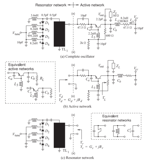
Figure \(\PageIndex{1}\): A \(5\text{ GHz}\) common-base SiGe BJT oscillator: (a) oscillator showing the interface (x-x) between the resonator network (also called a tank circuit) and the device; (b) active network; and (c) resonator network. The element labeled TL\(_{1}\) is a low impedance microstrip line. Capacitors \(C_{a}\) and \(C_{b}\) compensate for the frequency-dependent feedback provided by the base inductance. The choke inductor, \(L_{\text{CHOKE}} = 8.2\text{ nH}\), presents an RF open circuit and is part of the bias circuit. \(V_{CC} = 30\text{ V}\) and \(I_{CC} = 30\text{ mA}\). Each varactor diode \((D_{1}–D_{4})\) is model JDS2S71E. The transistor is a Si BJT model NE894M13, which is designed for oscillator applications above \(3\text{ GHz}\).
magnitude of \(3\:\Omega\) at \(5\text{ GHz}\) and are effectively RF short circuits.
The base inductor, \(L_{3}\), provides feedback that results in negative conductance from the emitter to ground. Since the feedback is frequency dependent, this induced negative conductance is also frequency dependent.
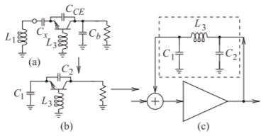
Figure \(\PageIndex{2}\): Transformation of the oscillator of Figure \(\PageIndex{1}\) into the form of a standard Colpitts feedback oscillator: (a) first stage of transformation combining the equivalent active and resonator networks in Figure \(\PageIndex{1}\); (b) combining \(L_{1}\) and \(C_{x}\) (due to \(C_{a}\) and parasitics) to obtain an equivalent capacitance \(C_{1}\); and (c) final feedback form (compare with the circuits in Figures 5.2.2(a) and 5.2.3(b)).
However, the reactive loading by \(C_{a}\) and \(C_{b}\) modifies the effective device conductance so that it becomes frequency independent. The design of \(C_{a}\) and \(C_{b}\) will be considered in depth later. The capacitors \(C_{a}\) and \(C_{b}\) are key to presenting an admittance to the resonator network that has the required characteristics for stable oscillation.
The resonator network, to the left of (\(\mathsf{x-x}\)) in Figure \(\PageIndex{1}\)(a), consists of a transmission line TL\(_{1}\) that is coupled to a variable capacitance provided by the stack of four varactors. A single varactor would provide a voltage-tunable capacitance, but the stack of four varactors allows a four-times-larger RF voltage swing [20]. The \(3.6\text{ nH}\) and \(8.2\text{ nH}\) inductors provide DC shorts while presenting RF open circuits. The tapped transmission line, referring to the connection between the active and resonator networks not being at the top of the transmission line, improves the loaded \(Q\) of the resonator network. The resonator network is resonant at a frequency below the oscillation frequency, with the transmission line being inductive at the oscillation frequency. So at the oscillation frequency the resonator network presents an inductance with the required slope of admittance with respect to frequency\(^{1}\). The design of the varactor stack is discussed further in Section 5.3 of [21].
The layout and populated microstrip circuit board are shown in Figure \(\PageIndex{3}\)(a and b). The resonator network is shown in Figure \(\PageIndex{4}\)(a) and the active network is shown in Figure \(\PageIndex{4}\)(b). Note the many vias to the backing ground plane. This is typical of microwave designs, as the vias eliminate substrate modes and the large grounded regions minimize parasitic coupling. The wide microstrip resonator, TL\(_{1}\), is seen in Figure \(\PageIndex{4}\)(a) and there is a shorting bar (available in chip form as a \(0\:\Omega\) resistor) across it to a ground strip. The bar can be repositioned and used to tune the resonator network. While this is necessary during manual oscillator design optimization, it is retained in the final design (as is usual). The shorting bar effectively reduces the length of TL\(_{1}\). At the output of the oscillator (see Figure \(\PageIndex{4}\)(b)) a Pi attenuator (with \(294\:\Omega\) resistors in the shunt legs and a \(17.4\:\Omega\) series resistor) is between \(V_{\text{out}}\) and the \(50\:\Omega\) bandpass filter. The filter blocks harmonics from the final output of the circuit. The impedance seen from the \(V_{\text{out}}\) terminal looking toward the filter is \(50\:\Omega\).
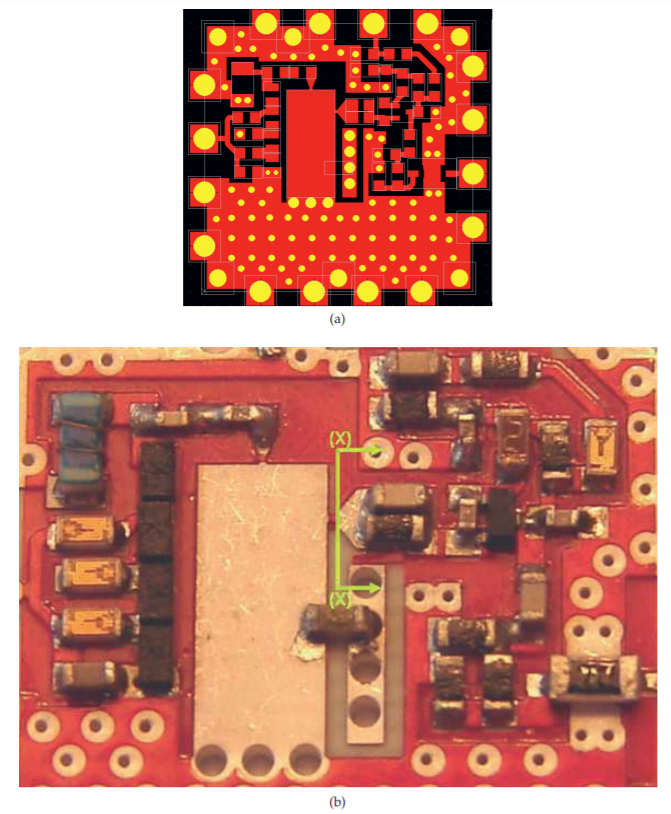
Figure \(\PageIndex{3}\): C-band VCO circuit: (a) layout showing metalization and vias to ground planes (in yellow); and (b) populated circuit board with the resonator network to the left of the cutaway line (\(\mathsf{x-x}\)) separated from the active circuit to the right.
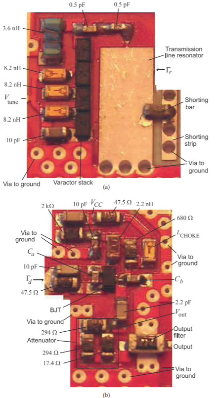
Figure \(\PageIndex{4}\): C-band VCO circuit: (a) annotated resonator network; and (b) annotated active network. The Pi attenuator (with \(294\:\Omega\) resistors in the shunt legs and a \(17.4\:\Omega\) series resistor) is between \(V_{\text{out}}\) and the \(50\:\Omega\) bandpass filter.
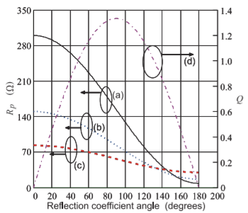
Figure \(\PageIndex{5}\): The resistance, \(R_{P}\), of a parallel (or shunt-tuned) resonator required to satisfy the condition of oscillation for (a) \(|\Gamma_{d}| = 1.4\), (b) \(|\Gamma_{d}| = 2\), and (c) \(|\Gamma_{d}| = 4\) versus the magnitude of the device reflection coefficient angle. Curve (d) is the active device \(Q = Q_{d} = |B_{d}/G_{d}|\) for \(|\Gamma_{d}| = 2\).
5.6.2 Design Strategy
Small-signal \(S\) parameters are generally good indicators of oscillator operation, particularly for the frequency of oscillation [22]. However, they do not provide sufficient information to determine if stable oscillation will occur. The design strategy here is to use simulations and measurements of the individual resonator and active networks to select the required modifications, particularly the selection of \(C_{a}\) and \(C_{b}\) and the position of the shorting bar. Measurements are needed as the characteristics are very sensitive to coupling parasitics, principally between the sides of the lumped elements, which cannot be captured in simulation.
5.6.3 Oscillator Start-Up Considerations
Another consideration in oscillator design is that the right conditions must be provided for oscillation start-up, which initially begins with the amplification of noise. Simply stated, the condition for oscillator start-up of a shunt-tuned oscillator is that for small signals (small \(A\)) \(|G_{d}(A, \omega )| > G_{r}(\omega )\). That is, for small signals, the active network must present a negative conductance that is greater in magnitude than the positive conductance of the resonator network. Since \(B_{d}(\omega)\approx −B_{r}(\omega )\), the condition for start-up of oscillation can also be expressed in terms of the \(Q\)s of the active and resonator networks. That is, for oscillation start-up, \(Q_{r} > Q_{d}\) for small signals where the \(Q\) of the active network is \(Q_{d} = |B_{d}/G_{d}|\) and the \(Q\) of the resonator network is \(Q_{r} = |B_{r}/G_{r}|\). Since \(G_{d}\) is negative, \(|\Gamma_{d}| > 1\), however, it is not sufficient to simply have a large value of \(|\Gamma_{d}|\).
There is a specific angular range of \(\Gamma_{d}\) that provides the right condition for oscillator start-up. Now \(1/\Gamma_{d}\approx\Gamma_{r}\) at steady-state oscillation and so designing for a particular \(\Gamma_{d}\) also determines \(\Gamma_{r}\). It is found that the angle of \(\Gamma_{d}\), \(\angle\Gamma_{d}\), must be constrained so that losses in the resonator network are accommodated. The appropriate range is selected using Figure \(\PageIndex{5}\), which plots the required minimum parallel resistance, \(R_{p} (= 1/G_{r})\), of the resonator network as a function of \(|\angle \Gamma_{d}|\) for several values of \(|\Gamma_{d}|\). If \(|\angle\Gamma_{d}|\) is less than \(50^{\circ}\), then the resonator network would need to have a higher \(Q\), \(Q_{r}\), in order to satisfy the oscillator start-up requirement. Now if a large tuning range of the VCO is required, then a large range of \(\angle\Gamma_{d}\) must be considered. A reasonable range derived from Figure \(\PageIndex{5}\) is that \(\angle\Gamma_{d}\) between \(30^{\circ}\) and \(70^{\circ}\) should be supported. Thus, in the case of a shunt-tuned oscillator, the design of the interface of the resonator and active networks is a methodical process to provide an appropriate admittance to enable oscillator start-up over the tuning bandwidth of the VCO.
What the above means is that if the active network is designed to present a negative conductance and little susceptance (so that \(\angle\Gamma_{d}\approx 180^{\circ}\)) to the resonator network, then the equivalent parallel resistance, \(R_{p}\), of the resonator network needs to be very high to ensure start-up. A high \(R_{p}\) means that the \(Q\) of the resonator network, \(Q_{r}\), must be high. However such a high \(Q_{r}\) would be difficult to achieve with a tunable resonator. To provide for greater likelihood of oscillator start-up as well as achievable \(Q_{r}\), it is better for the active network to present \(\angle\Gamma_{d}\approx 50^{\circ}\). The wide tuning range requirement extends this range to something like \(30^{\circ}\leq\angle\Gamma_{d}\leq 70^{\circ}\). It is thus not reasonable to simply embed reactances in the resonator network to compensate for parasitics in the active network and then to expect that the required start-up conditions be achieved. It may be possible to do this, but this approach would limit the ability to make other tradeoffs that would optimize oscillator performance. So the point is that better oscillator performance can be achieved by going beyond the simple form of the Kurokawa oscillation condition embodied in Equation 5.5.2.
With a fixed-frequency common-base Colpitts oscillator the oscillation operating point (the intersection of \(\Gamma_{r}\) and \(1/\Gamma_{d}\)) can be in the left-half plane of the Smith chart as the loss of the resonator is negligible. However with a microwave VCO the resonator loss, due to the varactors, is appreciable and the location of the intersection of \(\Gamma_{r}\) and \(1/\Gamma_{d}\) is important.
In summary, designing for a slightly reactive \(\Gamma_{d}\) is a subtle point that leads to a VCO design of superior performance. It is not necessary to understand this issue to follow the design procedure that follows. It is sufficient to follow the VCO design procedure by noting that one of the requirements is that \(30^{\circ}\leq |\angle\Gamma_{d}|\leq 70^{\circ}\), that is, the input admittance of the active network at the resonator-active network interface should be slightly capacitive (or slightly inductive). In matching \(1/\Gamma_{d}\) to \(\Gamma_{r}\), this corresponds to a slightly inductive (or slightly capacitive) resonator network with \(70^{\circ}\geq\angle\Gamma_{r}\geq 30^{\circ}\) (or \(−70^{\circ}\leq\angle\Gamma_{r}\leq −30^{\circ}\)).
5.6.4 Initial Design
The initial design of the oscillator with \(C_{a} = 0.5\text{ pF}\) and with \(C_{b} = 0\) resulted in the simulated resonator and active network characteristics shown in Figure \(\PageIndex{6}\), where the locus of \(\Gamma_{r}\) at two bias voltages, \(1\text{ V}\) and \(3\text{ V}\), are shown. Also shown are the small-signal characteristics of the active network, plotted as \(1/\Gamma_{d}\), and determined (in harmonic balance simulation) using a \(50\:\Omega\) port. The port impedance was high enough to suppress oscillation. The \(1/\Gamma_{d}\) curve intersects with each of the resonator curves at multiple places so that multiple oscillations are possible.
The similar measured characteristics of the actual oscillator are shown in Figure \(\PageIndex{7}\). The resonator network is shown to the left of the (\(\mathsf{x-x}\)) line in the oscillator schematic of Figure \(\PageIndex{1}\)(a) and again in Figure \(\PageIndex{1}\)(c). It is also shown in Figure \(\PageIndex{4}\)(a). Measurement of the tank circuit yielded the set of resonator curves (Curves a–g) in Figure \(\PageIndex{7}\). Curve a is the locus of the
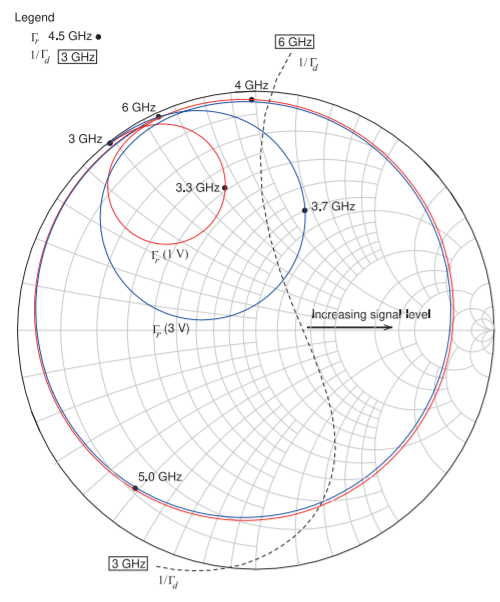
Figure \(\PageIndex{6}\): Simulated \(50\:\Omega\) reflection coefficient of the resonator, \(\Gamma_{r}\), and the inverse of the small-signal reflection coefficient of the active network, \(1/\Gamma_{d}\), of the C-band VCO with \(C_{a} = 0.5\text{ pF}\) and without \(C_{b}\). This is a \(50\:\Omega\) Smith chart.
reflection coefficient of the resonator network when the tuning voltage is \(0\text{ V}\), that is, Curve a is the locus with respect to frequency of \(\Gamma_{r}(0\text{ V})\). The seven resonator responses shown in Figure \(\PageIndex{7}\), Curves a–g, are the resonator reflection coefficients for equally spaced tuning voltages from \(0\text{ V}\) through \(9\text{ V}\). Comparing Figures \(\PageIndex{6}\) and \(\PageIndex{7}\) it is seen that there is reasonable agreement between the simulated and measured results. The difference can be attributed to the difficulty of performing the measurements at the correct location, as well as coupling between the components themselves not being captured in simulation.
The possibility of multiple oscillations is seen in Figures \(\PageIndex{6}\) and \(\PageIndex{7}\), as there can be multiple intersections of a \(\Gamma_{r}\) curve (for a particular bias) and the \(1/\Gamma_{d}\) curve. (Note that the \(1/\Gamma_{d}\) locus will shift to the right as the level of the oscillation signal increases.) Multiple oscillations are observed as seen in the spectrum at the output, \(V_{\text{out}}\), of the oscillator (see Figure \(\PageIndex{8}\)). An oscillator that oscillates at multiple frequencies is not desirable, of course, so the design must be altered to avoid the multiple intersections of the \(\Gamma_{r}\) (at a particular tuning voltage) and \(1/\Gamma_{d}\) curves.
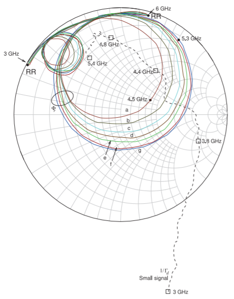
Figure \(\PageIndex{7}\): Measured reflection coefficient of the resonator network, \(\Gamma_{r}\), and the inverse of the small-signal reflection coefficient of the active device network, \(1/\Gamma_{d}\), of the C-band VCO with \(C_{a} = 0.5\text{ pF}\) and without \(C_{b}\). \(\Gamma_{r}\), Curve a, is the characteristic of the resonator network for a tuning voltage, \(V_{\text{tune}}\), of \(0\text{ V}\). Curve g is for \(V_{\text{tune}} = 9\text{ V}\). \(V_{\text{tune}}\) is equally spaced for Curves a–g. The locus of \(1/\Gamma_{d}\) moves to the right as the signal level increases and the intersection of \(1/\Gamma_{d}\) and \(\Gamma_{r}\) determines the oscillation frequency and the signal level.
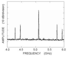
Figure \(\PageIndex{8}\): Multiple oscillations observed prior to reflection coefficient shaping by \(C_{a}\) and \(C_{b}\). The spectrum was measured using a resolution bandwidth of \(3\text{ MHz}\) and a video bandwidth of \(1\text{ MHz}\).
5.6.5 Avoiding Multiple Oscillations Through Reflection Coefficient Shaping
At an early stage in design (with \(C_{a} = 0.5\text{ pF}\) and \(C_{b} = 0\)) multiple oscillations were observed in Figure \(\PageIndex{8}\). The cause of these multiple oscillations is multiple intersections of the \(1/\Gamma_{d}\) locus of the active circuit and \(\Gamma_{r}\) at a particular bias voltage. This is seen in both the simulated results in Figure \(\PageIndex{6}\) and the measured results in Figure \(\PageIndex{7}\). The next step in design is to shape \(1/\Gamma_{d}\) of the active network so that there is a unique intersection
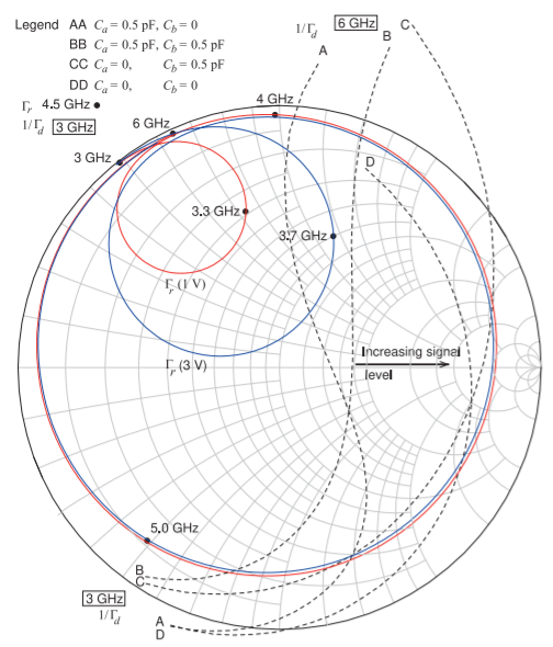
Figure \(\PageIndex{9}\): Simulated reflection coefficient of the resonator, \(\Gamma_{r}\), and the inverse of the small-signal reflection coefficient of the active network, \(1/\Gamma_{d}\), of the C-band VCO for various values of the compensation capacitors \(C_{a}\) and \(C_{b}\).
of \(1/\Gamma{d}\) and \(\Gamma_{r}\) at each bias voltage. The elements used to shape \(1/\Gamma_{d}\) are \(C_{a}\) and \(C_{b}\). At the same time that these are adjusted the design must achieve \((\partial B_{d}/\partial V|_{V =V_{0}})\approx 0\). Also, the discussion in Section 5.6.3 indicated that the preferred angle of \(\Gamma_{d}\) to ensure start-up of oscillations is around \(50^{\circ}\). However, for a wide tuning range of the VCO it is only possible to achieve a specific angle of \(\Gamma_{d}\) at a single oscillation frequency. The trade-off is to choose \(−70^{\circ}\leq\angle\Gamma_{d}\leq −30^{\circ}\), indicating that the active network should be slightly capacitive, which corresponds to a slightly inductive resonator network with \(70^{\circ}\geq\angle\Gamma_{r}\geq 30^{\circ}\). Thus the intersection of \(\Gamma_{r}\) and \(1/\Gamma_{d}\) should be in the top right quadrant of the Smith chart. (An alternative design choice which still would have resulted in a successful start-up of the oscillator is \(70^{\circ}\geq\angle\Gamma_{d}\geq 30^{\circ}\).)
The simulated characteristics of the resonator and active networks are shown in Figure \(\PageIndex{9}\). The loci of \(\Gamma_{r}\) for two tuning voltages are shown, and the small-signal \(1/\Gamma_{d}\) is shown for various values of \(C_{a}\) and \(C_{b}\). Curve AA (of \(1/\Gamma_{d}\)) is for \(C_{a} = 0.5\text{ pF}\) and \(C_{b} = 0\), as considered before, and will resulted in multiple oscillations. Curve DD is for \(C_{a} = 0\) and \(C_{b} = 0\) and is very close to \(\Gamma_{r}\) and it may be difficult for oscillation to begin. Another way of describing this is that \(Q_{r}\) is very close to the small-signal \(Q_{d}\). So even if oscillation did start, it would reach steady state at a low signal level. The active networks represented by Curves CC and DD do not provide sufficient
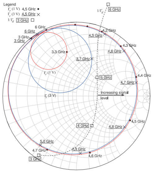
Figure \(\PageIndex{10}\): Simulated reflection coefficient of the resonator, \(\Gamma_{r}\), and the inverse of the small-signal reflection coefficient of the active network, \(1/\Gamma_{d}\), of the C-band VCO.
negative conductance and only enable oscillation over a narrow frequency range. The best characteristic here is Curve BB for which \(C_{a} = 0.5\text{ pF}\) and \(C_{b} = 0.5\text{ pF}\). This response provides a single intersection of the resonator curve for each tuning voltage and the active network curve. Also it indicates a fairly large magnitude of negative conductance so that the output oscillator power will be high. That is, the magnitude of the negative conductance reduces as the signal level increases and the large magnitude of the negative conductance at small signals means the signal level can grow significantly before the conductances of the resonator and active networks match.
The simulated characteristics of the resonator and active networks are repeated in Figure \(\PageIndex{10}\) for \(C_{a} = 0.5\text{ pF}\) and \(C_{b} = 0.5\text{ pF}\) (i.e. Curve BB in Figure \(\PageIndex{9}\)). The response of the circuit now has the desired properties. First consider the locus of the reflection coefficient of the resonator network with \(1\text{ V}\) across the varactor diodes (this is the \(\Gamma_{r}(1\text{ V})\) curve). There are two resonances between \(3\text{ GHz}\) and \(6\text{ GHz}\), but it is the resonance between \(4.0\text{ GHz}\) and \(5.3\text{ GHz}\) that is close to the \(1/\Gamma_{d}\) locus and so (for this varactor bias) is the only resonance that will affect oscillation. The locus of \(\Gamma_{r}(1\text{ V})\) approximately follows a constant conductance curve so that \((\partial G_{r}/\partial\omega|_{\omega=\omega_{0}})\approx 0\) as required. As the signal level across the active network increases, the \(1/\Gamma_{d}\) locus shifts to the right in the direction of constant susceptance so that \((\partial B_{d}/\partial V|_{V =V_{0}})\approx 0\) as desired. Provided that the frequencies match, the point at which the \(\Gamma_{r}(1\text{ V})\) locus intersects the \(1/\Gamma_{d}\) locus determines both the oscillation frequency and the oscillation level as
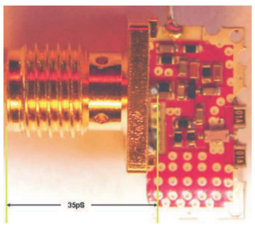
Figure \(\PageIndex{11}\): Measurement of the active circuit with a \(50\:\Omega\) test fixture at the interface of the resonator and active networks. The card was cut at the interface to make the connection. A \(35\text{ ps}\) delay due to the length of the SMA connector must be subtracted from measurements to reference measurements to the circuit card edge.
the locus of \(1/\Gamma_{d}\) shifts to the right.
The simulated results discussed in the previous paragraph indicate that the oscillator will work as desired. However, there are many parasitics and coupling effects that are not fully captured in simulation. Final design optimization requires experimental investigation of the reflection coefficients looking into the resonator circuit and into the active circuit.
The next step in design of the VCO is using a VNA to measure the reflection coefficient of the active network in Figures \(\PageIndex{1}\)(b) and \(\PageIndex{4}\)(b) (shown again in its measurement configuration in Figure \(\PageIndex{11}\)). The large signal locus in Figure \(\PageIndex{12}\) was measured with a \(10\text{ dBm}\) signal applied to the active network at the \(50\:\Omega\) measurement port. This curve is an indication of what the active network presents to the resonator under large signal conditions and it is used as a guide since it does not capture the full loading complexity, for example, the harmonic terminations are not correct.
Oscillation occurs when the characteristics of the active network (see the \(1/\Gamma_{d}\) curve in Figure \(\PageIndex{12}\)) match the characteristic of the resonator network, Curves a–g in Figure \(\PageIndex{12}\). First, for small signals the active network should provide
\[\label{eq:1}|1/\Gamma_{d}(A,\omega )|<|\Gamma(\omega)| \]
at all desired frequencies of operation. This is the requirement for oscillation start-up. Second, the rotation of \(\Gamma_{r}(\omega )\) with respect to \(\omega\) near the oscillation point (i.e., \(\omega_{0}\)) should be positive (i.e., \((\partial B_{r}/\partial\omega |_{\omega =\omega_{0}}) > 0\) as developed in Section 5.5.2) and in the opposite direction to the \(1/\Gamma_{d}(A, \omega )\) locus with respect to \(\omega\) (i.e., in the same direction as the rotation of \(\Gamma_{d}(A, \omega )\)). This is indeed what happens and can be seen by closer examination of Curves a–g. In addition, the locus of \(\Gamma_{r}(\omega )\) should approximately follow a line of constant conductance so that \((\partial G_{r}/\partial\omega |_{\omega=\omega_{0}})\approx 0\). Now, device self-limiting stabilizes oscillation when the angles of \(\Gamma_{d}(A,\omega )\) and \(\Gamma_{r}(\omega )\) sum to zero. For single-frequency oscillation this must be obtained at each tuning voltage. Finally, the trajectory of the limiting \(1/\Gamma_{d}(A, \omega )\) locus (i.e as the amplitude of oscillation, \(A\) or \(V\), increases) should intersect the \(\Gamma_{r}(\omega )\) locus, ideally at right angles to minimize phase noise [11, 17]. These requirements are referred to as a complementary relationship between the active and resonator networks.
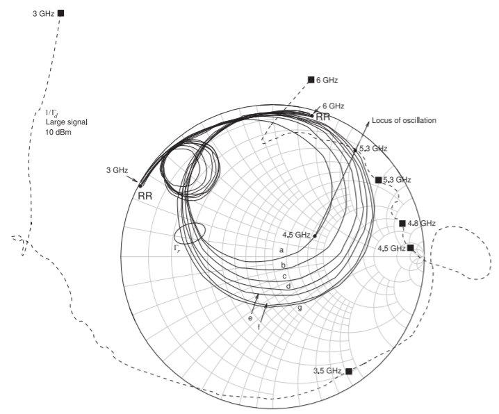
Figure \(\PageIndex{12}\): Measured reflection coefficient of the resonator network, \(\Gamma_{r}\), and the inverse of the large signal reflection coefficient of the active network, \(1/\Gamma_{d}\), of the C-band VCO. For the large signal \(\Gamma_{d}\) measurement, the active network is driven at \(10\text{ dBm}\) from a \(50\:\Omega\) port. The \(\Gamma_{r}\) curves are identical to those in Figure \(\PageIndex{7}\). The curves with end points labeled RR identify the resonator curves.
While under small-signal conditions the loci may not coincide, the important point is that they do when limiting occurs, as well as providing for the start-up of oscillation. A slight counterclockwise rotation of the modified active device \(1/\Gamma_{d}\) locus as the signal level increases (as well as a general right shift) ensures stable, single-frequency oscillation. Put another way, the trajectory of the negative conductance as device limiting occurs must be such that \(1/\Gamma_{d}\) just intersects the \(\Gamma_{r}\) locus, and \(\angle\Gamma_{d}\) must complement \(\angle\Gamma_{r}\). This is the situation shown in Figure \(\PageIndex{12}\), where the modified device network characteristic is achieved by adding capacitive terminations to the collector and the emitter base terminals. Here, unlike the conventional common-base series feedback oscillator situation (as considered in Section 5.4), the input of the active network is now capacitive above \(4.5\text{ GHz}\) (see Figure \(\PageIndex{12}\)). Consequently the inductance of the resonator is successfully absorbed. Thus
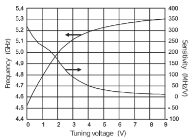
Figure \(\PageIndex{13}\): Measured tuning characteristic showing oscillation frequency and VCO sensitivity as a function of tuning voltage.
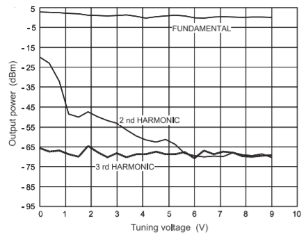
Figure \(\PageIndex{14}\): Measured output power and harmonics at \(V_{\text{out}}\) (before the bandpass filter) indicating low-level harmonic content.
the small-signal one-port reflection coefficient of the resonator is inductive initially. In effect the resonator is operated as a tunable shunt inductance rather than a tunable capacitive reactance.
5.6.6 VCO Performance
The most important metrics that describe the performance of the VCO are the phase noise, tuning bandwidth, output power, tuning gain or sensitivity, the output harmonic content, and the DC power consumption. The VCO characterized here, shown in Figure \(\PageIndex{1}\), includes the compensating capacitors \(C_{a}\) and \(C_{b}\), both \(0.5\text{ pF}\). Figures \(\PageIndex{13}\) and \(\PageIndex{14}\) document the bandwidth and output powers of the VCO. As the varactor tuning voltage, \(V_{\text{tune}}\), goes from \(0\text{ V}\) to \(9\text{ V}\) the filter tunes from \(4.5\text{ GHz}\) to \(5.3\text{ GHz}\), producing a minimum output power of \(0\text{ dBm}\) and varies by no more than \(2\text{ dB}\) over the range. The DC power consumed is \(150\text{ mW}\). The tuning bandwidth is adjusted by varying the coupling (provided by the two \(0.5\text{ pF}\) capacitors) between the varactor stack and the microstrip line, TL\(_{1}\). Figure \(\PageIndex{14}\) also shows the power at the harmonics. At the final output these are further reduced by the bandpass filter.
The measured phase noise is shown in Figure \(\PageIndex{15}\) at \(4.5\text{ GHz}\)
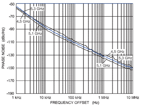
Figure \(\PageIndex{15}\): Phase noise measured at the top and bottom of the tuning range as well as at \(5.1\text{ GHz}\), where phase noise is optimum. Minimum phase noise floor \(−116\text{ dBc/Hz}\) at \(1\text{ kHz}\) offset, \(−160\text{ dBc/Hz}\) at \(10\text{ MHz}\) offset.
(corresponding to a tuning voltage of \(0\text{ V}\)), and at \(5.3\text{ GHz}\) (a tuning voltage of \(9\text{ V}\)), as well as at \(5.1\text{ GHz}\) where the best phase noise is obtained. The phase noise is approximately the same across the tuning range with a \(1/f^{2}\) noise corner frequency, \(f_{c,−2}\) (the transition from an \(f^{−1}\) dependency to an \(f^{−2}\) dependency) of \(30\text{ kHz}\). The phase noise at \(10\text{ kHz}\) offset, \(\mathcal{L}(10\text{ kHz})\), is better than \(−85\text{ dBc/Hz}\), while \(\mathcal{L}(1\text{ MHz})\) is better than \(−130\text{ dBc/Hz}\). The best measured phase noise, \(\mathcal{L}(1\text{ MHz})\), near band center \((5.1\text{ GHz})\) is \(−135\text{ dBc/Hz}\).
The performance of a VCO should be quoted as the worst performance over the tuning bandwidth. For a tuning bandwidth of \(770\text{ MHz}\) and center frequency of \(4.92\text{ GHz}\), the maximum phase noise of this VCO is \(−128\text{ dBc/Hz}\). This improves to a maximum phase noise of \(−130\text{ dBc/Hz}\) for a bandwidth of \(500\text{ MHz}\) centered at \(5.05\text{ GHz}\).
5.6.7 Summary
The VCO design here used a standard one-port reflection oscillator design approach with a technique that introduced compensation capacitors to manage the otherwise frequency-dependent susceptance of the active network. These compensation elements also resulted in the reflection coefficient of the augmented active device having the characteristics necessary to ensure stable oscillation and oscillator start-up.
Footnotes
[1] The resonator could be adjusted to present a capacitive susceptance.