2.5: EFFECTS OF FEEDBACK ON INPUT AND OUTPUT IMPEDANCE
- Page ID
- 59331

The gain-stabilizing and linearizing effects of feedback have been described earlier in this chapter. Feedback also has important effects on the input and output impedances of an amplifier, with the type of modification dependent on the topology of the amplifier-feedback network combination.
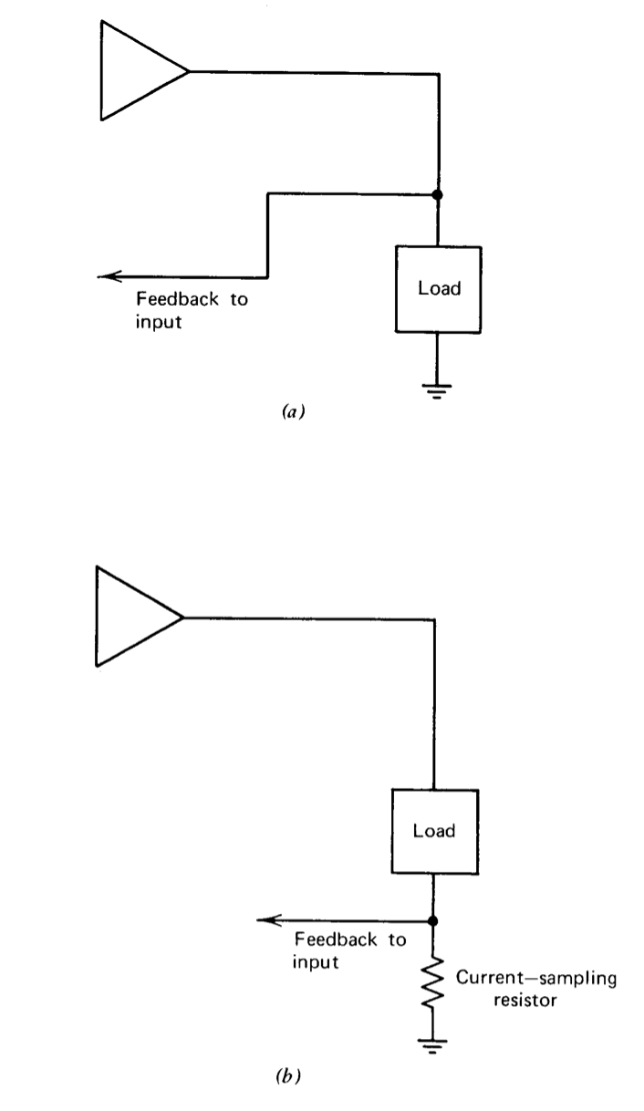
Figure 2.15 shows how feedback might be arranged to return information about either the voltage applied to the load or the current flow through it. It is clear from physical arguments that these two output topologies must alter the impedance facing the load in different ways. If the information fed back to the input concerns the output voltage, the feedback tends to reduce changes in output voltage caused by disturbances (changes in load current), thus implying that the output impedance of the amplifier shown in Figure 2.15\(a\) is reduced by feedback. Alternatively, if information about load current is fed back, changes in output current caused by disturbances(changes in load voltage) are reduced, showing that this type of feedback raises output impedance.
Two possible input topologies are shown in Figure 2.16. In Figure 2.16\(a\), the input signal is applied in series with the differential input of the amplifier. If the amplifier characteristics are satisfactory, we are assured that any required output signal level can be achieved with a small amplifier input current. Thus the current required from the input-signal source will be small, implying high input impedance. The topology shown in Figure 2.16\(b\) reduces input impedance, since only a small voltage appears across the parallel input-signal and amplifier-input connection.
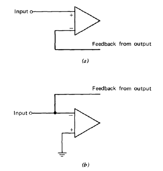
Figure 2.16 Two possible input topologies. (\(a\)) Input signal applied in series with amplifier input. (\(b\)) Input signal applied in parallel with amplifier input.
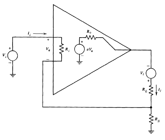
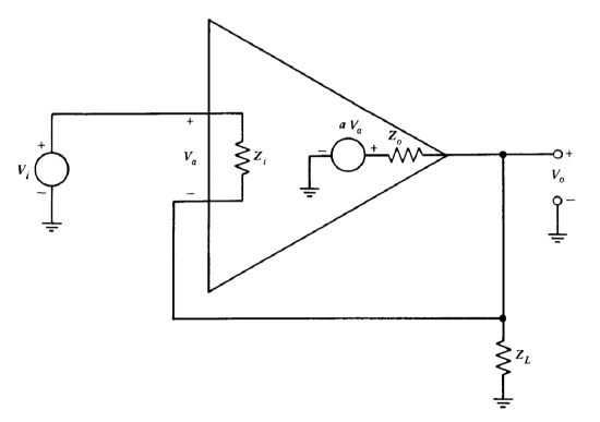
Figure 2.17 Amplifier with high input and output resistances.
The amount by which feedback scales input and output impedances is directly related to the loop transmission, as shown by the following example. An operational amplifier connected for high input and high output resistances is shown in Figure 2.17. The input resistance for this topology is simply the ratio \(V_i/I_i\). Output resistance is determined by including a voltage source in series with the load resistor and calculating the ratio of the change in the voltage of this source to the resulting change in load current, \(V_l/I_l\). If it is assumed that the components of \(I_l\) and the current through the sampling resistor \(R_S\) attributable to \(I_i\) are negligible (implying that the amplifier, rather than a passive network, provides system gain) and that \(R_i \gg R_s\), the following equations apply.
\[V_a = V_i - R_S I_l \nonumber \]
\[I_l = \dfrac{aV_a + V_l}{R_o + R_L + R_S} \nonumber \]
\[I_i = \dfrac{V_a}{R_i} \nonumber \]
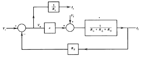
These equations are represented in block-diagram form in Figure 2.18. This block diagram verifies the anticipated result that, since the input voltage is compared with the output current sampled via resistor \(R_S\), the ideal trans-conductance (ratio of \(I_l\) to \(V_i\)) is simply equal to \(G_S\). The input resistance is evaluated by noting that
\[\dfrac{I_i}{V_i} = \dfrac{1}{R_{in}} = \dfrac{1}{R_i \{1 + [aR_S/(R_o + R_L + R_S)]\}}\label{eq2.5.5} \]
or
\[R_{in} = R_i \left (1 + \dfrac{aR_S}{R_o + R_L + R_S} \right ) \nonumber \]
The output resistance is determined from(Note that the output resistance in this example is calculated by including a voltage source in series with the load resistor. This approach is used to emphasize that the loop transmission that determines output resistance is influenced by \(R_L\). An alternative development might evaluate the resistance facing the load by replacing \(R_L\) with a test generator.)
\[\dfrac{I_l}{V_l} = \dfrac{1}{R_{out}} = \dfrac{1}{(R_o + R_L + R_S) \{1 + [aR_S/(R_o + R_L + R_S)]\}} \nonumber \]
yielding
\[R_{out} = (R_o + R_L + R_S) \left (1 + \dfrac{aR_S}{R_o + R_L + R_S} \right ) \label{eq2.5.7} \]
The essential features of Equations \(\ref{eq2.5.5}\) and \(\ref{eq2.5.7}\) are the following. If the system has no feedback (e.g., if \(a = 0\)), the input and output resistances become
\[R_{in}' = R_i \nonumber \]
and
\[R_{out}' = R_o + R_L + R_S \nonumber \]
Feedback increases both of these quantities by a factor of \(1 + [aR_S/ (R_o + R_L + R_S)]\), where \(-aR_S/(R_o + R_L + R_S)\) is recognized as the loop transmission. Thus we see that the resistances in this example are increased by the same factor (one minus the loop transmission) as the desensitivity increase attributable to feedback. The result is general, so that input or output impedances can always be calculated for the topologies shown in Figs. 2.15 or 2.16 by finding the impedance of interest with no feedback and scaling it (up or down according to topology) by a factor of one minus the loop transmission.
While feedback offers a convenient method for controlling amplifier input or output impedances, comparable (and in certain cases, superior) results are at least conceptually possible without the use of feedback. Consider, for example, Figure 2.19, which shows three ways to connect an operational amplifier for high input impedance and unity voltage gain.
The follower connection of Figure 2.19\(a\) provides a voltage gain
\[\dfrac{V_o}{V_i} = \dfrac{a}{1 + a} \nonumber \]
or approximately unity for large values of \(a\). The relationship between input impedance and loop transmission discussed earlier in this section shows that the input impedance for this connection is
\[\dfrac{V_i}{I_i'} = Z_i (1 + a) \nonumber \]
The connection shown in Figure 2.19b precedes the amplifier with an impedance that, in conjunction with the input impedance of the amplifier, attenuates the input signal by a factor of \(1/(1 + a)\). This attenuation combines with the voltage gain of the amplifier itself to provide a composite voltage gain identical to that of the follower connection. Similarly, the series impedance of the attenuator input element adds to the input impedance of the amplifier itself so that the input impedance of the combination is identical to that of the follower.
The use of an ideal transformer as impedance-modifying element can lead to improved input impedance compared to the feedback approach. With a transformer turns ratio of \((a + 1): 1\), the overall voltage gain of the transformer-amplifier combination is the same as that of the follower connection, while the input impedance is
\[\dfrac{V_i}{I_i ''} = Z_i (1 + a)^2 \nonumber \]
This value greatly exceeds the value obtained with the follower for large amplifier voltage gain.
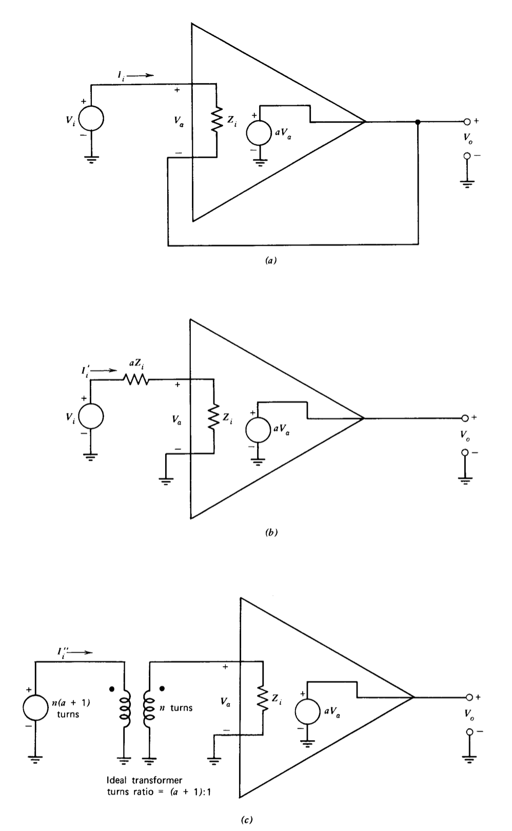
The purpose of the above example is certainly not to imply that attenuators or transformers should be used in preference to feedback to modify impedance levels. The practical disadvantages associated with the two former approaches, such as the noise accentuation that accompanies large input-signal attenuation and the limited frequency response characteristic of transformers, often preclude their use. The example does, however, serve to illustrate that it is really the power gain of the amplifier, rather than the use of feedback, that leads to the impedance scaling. We can further emphasize this point by noting that the input impedance of the amplifier connection can be increased without limit by following it with a step-up transformer and increasing the voltage attenuation of either the network or the transformer that precedes the amplifier so that the overall gain is one. This observation is a reflection of the fact that the amplifier alone provides infinite power gain since it has zero output impedance.
One rather philosophical way to accept this reality concerning impedance scaling is to realize that feedback is most frequently used because of its fundamental advantage of reducing the sensitivity of a system to changes in the gain of its forward-path element. The advantages of impedance scaling can be obtained in addition to desensitivity simply by choosing an appropriate topology.
PROBLEMS
Exercise \(\PageIndex{1}\)
Figure 2.20 shows a block diagram for a linear feedback system. Write a complete, independent set of equations for the relationships implied by this diagram. Solve your set of equations to determine the input-to-output gain of the system.
Exercise \(\PageIndex{2}\)
Determine how the fractional change in closed-loop gain
\[\dfrac{d(V_o/V_i)}{V_o/V_i}\nonumber \]
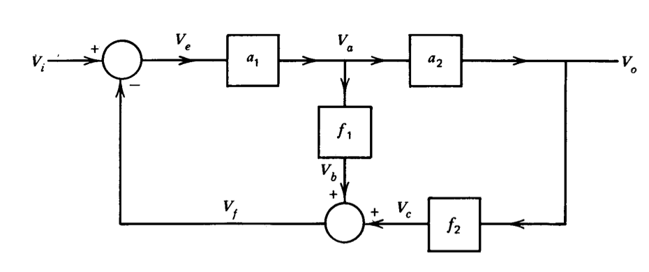
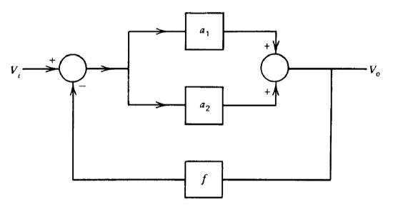
is related to fractional changes in \(a_1, a_2\), and \(f\) for the system shown in Figure 2.21.
Exercise \(\PageIndex{3}\)
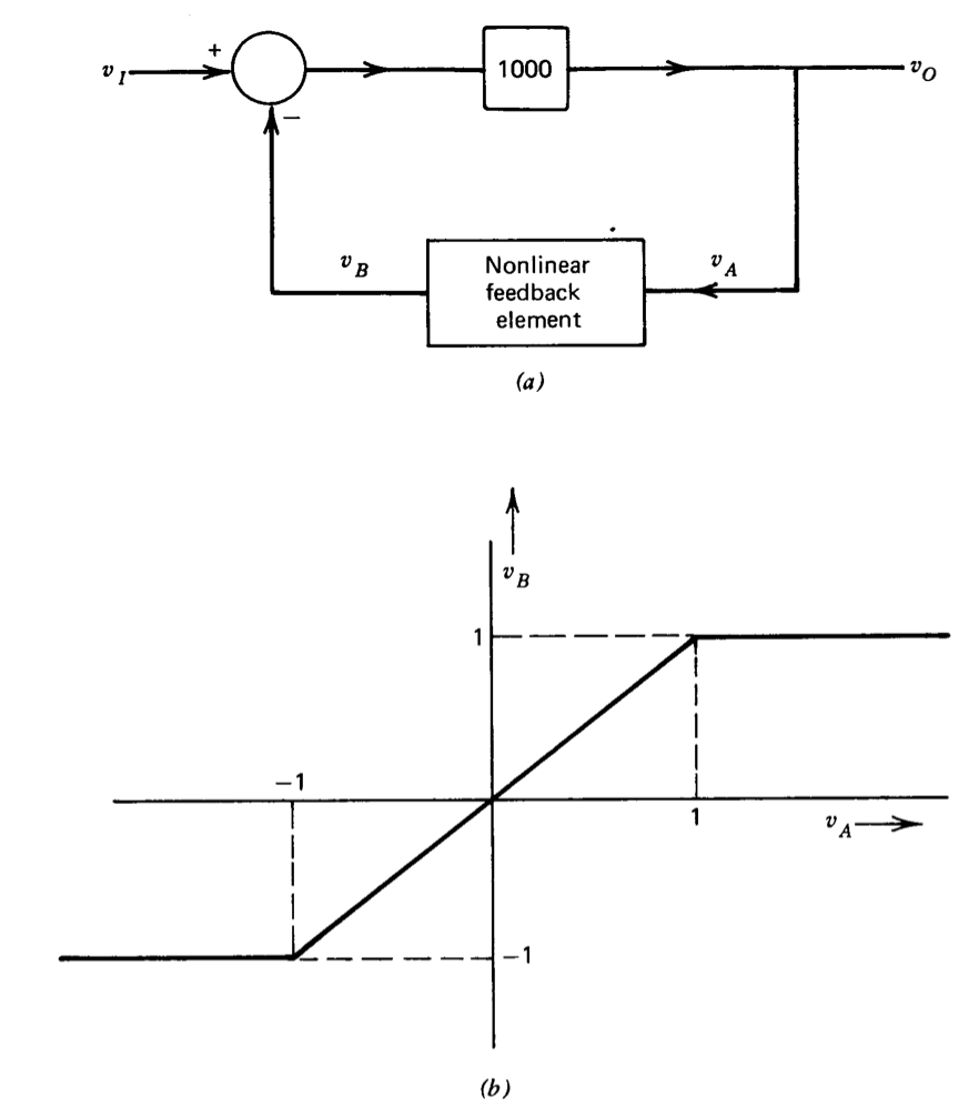
Plot the closed-loop transfer characteristics for the nonlinear system shown in Figure 2.22.
Exercise \(\PageIndex{4}\)
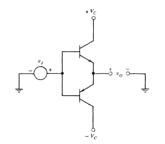
The complementary emitter-follower connection shown in Figure 2.23 is a simple unity-voltage-gain stage that has a power gain approximately equal to the current gain of the transistors used. It has nonlinear transfer characteristics, since it is necessary to apply approximately 0.6 volts to the base-to-emitter junction of a silicon transistor in order to initiate conduction.
(a) Approximate the input-output transfer characteristics for the emitter-follower stage.
(b) Design a circuit that combines this power stage with an operational amplifier and any necessary passive components in order to provide a closed-loop gain with an ideal value of +5.
(c) Approximate the actual input-output characteristics of your feedback circuit assuming that the open-loop gain of the operational amplifier is \(10^5\).
Exercise \(\PageIndex{5}\)
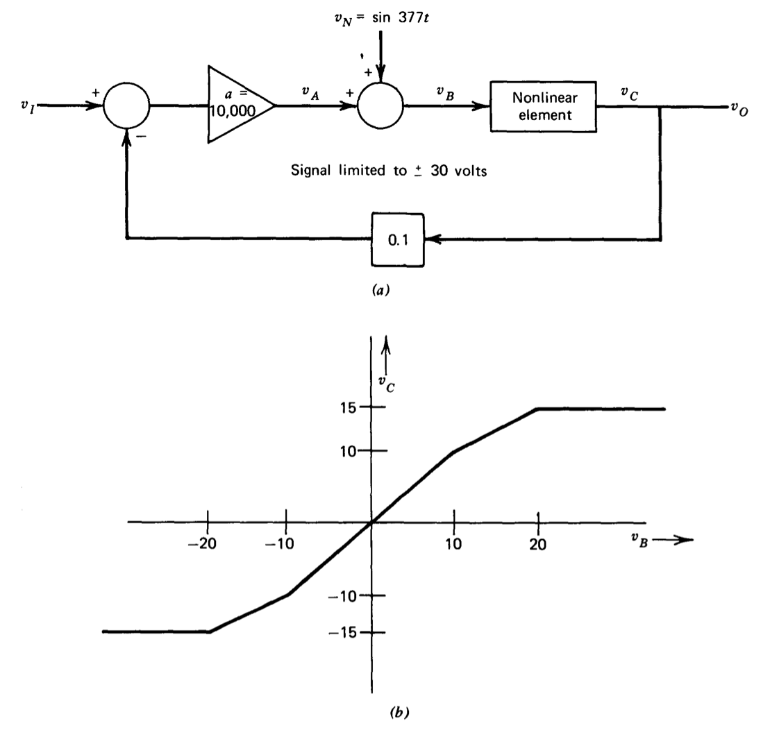
(a) Determine the incremental gain \(v_o/v_i\) for \(V_I = 0.5\) and 1.25 for the system shown in Figure 2.24.
(b) Estimate the signal \(v_A\) for \(v_I\), a unit ramp \([v_I (t) = 0, t < 0, = t, t > 0]\).
(c) For \(v_I = 0\), determine the amplitude of the sinusoidal component of \(v_O\).
Exercise \(\PageIndex{6}\)
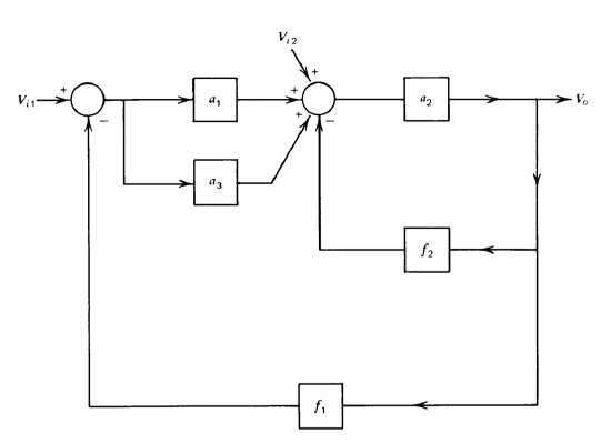
Determine \(V_o\) as a function of \(V_{i1}\) and \(V_{i2}\) for the feedback system shown in Figure 2.25.
Exercise \(\PageIndex{7}\)
Draw a block diagram that relates output voltage to input voltage for an emitter follower. You may assume that the transistor remains linear, and useahybrid-pi model for the device. Include elements \(r_{\pi}\), \(r_x\), \(C_{\pi}\), and \(C_{\mu}\), in addition to the dependent generator, in your model. Reduce the block diagram to a single input-output transfer function.
Exercise \(\PageIndex{8}\)
Draw a block diagram that relates \(V_o\) to \(V_i\) for the noninverting connection shown in Figure 2.26. Also use block-diagram techniques to determine the impedance at the output, assuming that \(Z_i\) is very large.
Exercise \(\PageIndex{9}\)
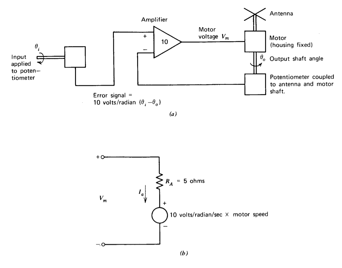
A negative-feedback system used to rotate a roof-top antenna is shown in Figure 2.27\(a\).
The total inertia of the output member (antenna, motor armature, and pot wiper) is 2 \(kg \cdot m^2\). The motor can be modeled as a resistor in series with a speed-dependent voltage generator (Figure 2.27\(b\)).
The torque provided by the motor that accelerates the total output-member inertia is 10 \(N \cdot m\) per ampere of \(I_a\). The polarity of the motor de pendent generator is such that it tends to reduce the value of \(I_a\), as the motor accelerates so that \(I_a\), becomes zero for a motor shaft velocity equal to \(V_m/10\) radians per second.
Draw a block diagram that relates \(\theta_o\) to \(\theta_i\). You may include as many intermediate variables as you wish, but be sure to include \(V_m\) and \(I_a\) in your diagram. Find the transfer function \(\theta_o/\theta_i\).
Modify your diagram to include an output disturbance applied to the antenna by wind. Calculate the angular error that results from a 1 \(N \cdot m\) disturbance.
Exercise \(\PageIndex{10}\)
Draw a block diagram for this set of equations:
\[\begin{array} {rcl} {W + X} & = & {3} \\ {X + Y} & = & {5} \\ {Y + Z} & = & {7} \\ {2W + X + Y + Z} & = & {11} \end{array}\nonumber \]
Use the block-diagram reduction equation (Equation 2.4.18) to determine the values of the four dependent variables.
Exercise \(\PageIndex{11}\)
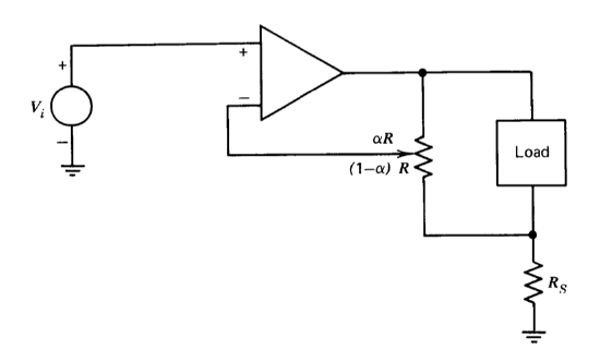
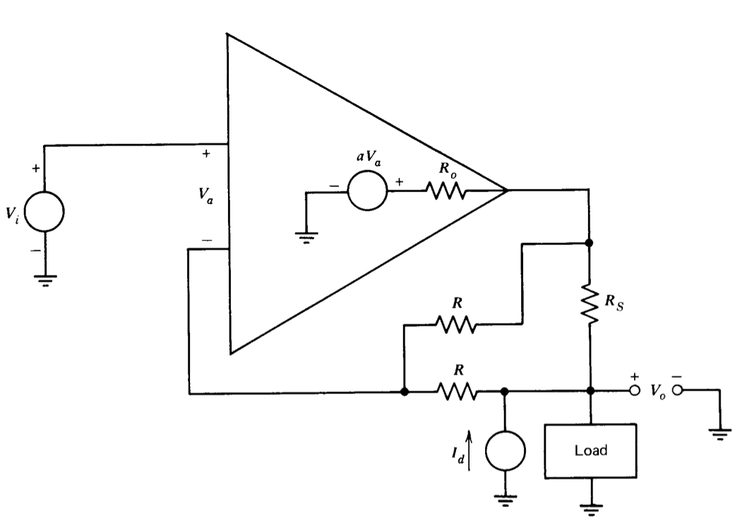
The connection shown in Figure 2.28 feeds back information about both load current and load voltage to the amplifier input. Draw a block dia gram that allows you to calculate the output resistance \(V_o/I_d\).
You may assume that \(R \gg R_S\) and that the load can be modeled as a resistor \(R_L\). What is the output resistance for very large \(a\)?
Exercise \(\PageIndex{12}\)
An operational amplifier connected to provide an adjustable output resistance is shown in Figure 2.29. Find a Thevenin-equivalent circuit facing the load as a function of the potentiometer setting a. You may assume that the resistance \(R\) is very large and that the operational amplifier has ideal characteristics.