
11.3: GENERAL PRECAUTIONS
- Page ID
- 58475

The operational amplifier is a complex circuit that is used in a wide variety of connections. Frequently encountered problems include amplifier destruction because of excessive voltages or power dissipation and oscillation. The precautions necessary to avoid these hazards depend on the specific operational amplifier being used. We generally find, for example, that discrete-component amplifiers are more tolerant of abuse than are inte grated-circuit units, since more sophisticated protective features are frequently included in discrete designs.
This section indicates some of the more common problem areas and suggests techniques that can be used to avoid them.
Destructive Processes
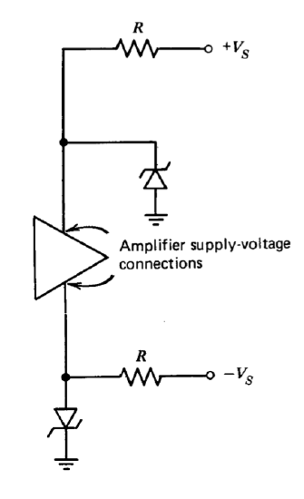
Excessive power-supply voltages are a frequent cause of amplifier damage. Isolation from uncertain supply-voltage levels via a resistor-Zener diode combination, as shown in Figure 11.6, is one way to eliminate this hazard. The Zener diodes also conduct in the forward direction in the event of supply-voltage reversal. A better solution in systems that include a large number of operational amplifiers is to make sure that the power supplies include "crowbar"-type protection that limits voltages to safe levels in the event of power-supply failure.
Excessive differential input voltage applied to an operational amplifier may damage the input-transistor pair. If input voltages in excess of about 0.6 volt are applied to a normal differential-amplifier connection, the base-to-emitter junction of one of the members of the pair will be reverse biased. Further increases in applied differential voltage eventually result in reverse breakdown.
The base-to-emitter junction can be burned out if sufficient power is applied to it. A more subtle problem, however, is that base-to-emitter reverse breakdown, even at low power levels, often irreversibly lowers the current gain of bipolar transistors. Thus the input current of an amplifier can be permanently increased by this mechanism. The potential for low power level base-to-emitter breakdown exists in many connections. Consider, for example, the usual integrator connection. If amplifier power is shut off with the feedback capacitor charged, the differential input voltage limit may be exceeded.
One practical solution is to include a pair of clamp diodes between the input terminals of the amplifier. Since the voltage between these terminals is nearly zero under normal operating conditions, the diodes have no effect until excessive voltage levels are reached.
Excessive power dissipation can result in some designs if the output terminal is shorted to ground. This possibility exists primarily in early integrated-circuit designs that do not include current-limiting circuits. More modern integrated-circuit designs, as well as most discrete circuits, are protected for output-to-ground shorts at normal supply-voltage levels and room-temperature operation. Some of these amplifiers are not protected for output shorts to either supply voltage, or output-to-ground shorts at elevated temperatures.
The compensation or balance terminals of operational amplifiers are frequently connected to critical low-level points, and any signal applied to
these terminals invites disaster. The author is particularly adept at demon strating this mode of destruction by shorting adjacent pins to each other or a pin to ground with an oscilloscope probe.
Oscillation
One of the most frequent complaints about operational amplifiers is that they oscillate in connections that the user feels should be stable. This phenomenon usually reflects a problem with the user rather than with the amplifier, and most of these instabilities can be corrected by proper design practice.
One frequent reason for oscillation is that dynamics associated with the load applied to the amplifier or the feedback network connected around it combine with the open-loop transfer function of the amplifier to produce feedback instabilities. The material presented in the chapters on feedback provides the general guidelines to eliminate these types of oscillations. Specific examples are given in Chapter 13.
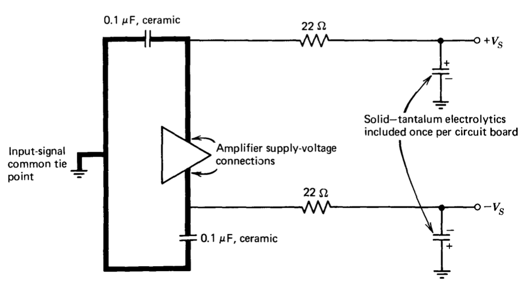
Another common cause of oscillation is excessive power-connection impedance. This problem is particularly severe with high-frequency amplifiers because of the inductance of the leads that couple the power supply to the amplifier. In order to minimize difficulties, it is essential to properly decouple or bypass all power-supply leads to amplifiers without internal decoupling networks. Good design practice includes using a fairly large value (\(>1\ \mu F\)) solid-tantalum electrolytic capacitor from the positive and the negative power supply to ground on each circuit board. Individual amplifiers should have ceramic capacitors (\(0.01\ \mu F\) to \(0.1\ \mu F\)) connected directly from their supply terminals to a common ground point. The single ground connection between the two decoupling capacitors should also serve as the tie point for the input-signal common, if possible. Lead length on both the supply voltage and the ground side of these capacitors is critical since series inductance negates their value. Ground planes may be mandatory in high-frequency circuits for acceptably low ground-lead inductance. If low supply currents are anticipated, crosstalk between amplifiers can be reduced by including small (\(\simeq 22 \Omega\)) series resistors in each decoupling network, as shown in Figure 11.7.
In addition to reducing supply-line impedance, decoupling networks often lower the amplitude of any supply-voltage transients. Such transients are particularly troublesome with amplifiers that use capacitive minor-loop feedback for compensation, since the feedback element can couple transients applied to a supply-voltage terminal directly to the amplifier output.
The open-loop transfer function of many operational amplifiers is dependent on the impedance connected to the noninverting input of the amplifier. In particular, if a large resistor is connected in series with this terminal (possibly to balance resistances seen at both inputs, thus reducing effects of bias currents), the bandwidth of the amplifier may deteriorate, leading to oscillation. In these cases a capacitor should be used to shunt the non- inverting input of the amplifier to the common input-signal and power-sup ply-decoupling ground point.
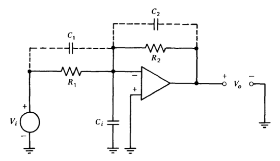
The input capacitance of an operational amplifier may combine with the feedback network to introduce a pole that compromises stability. Figure 11.8 is used to illustrate this problem. It is assumed that the input conductance of the amplifier is negligibly small, and that its input capacitance is modeled by the capacitor \(C_i\) shown in Figure 11.8. If the capacitors shown with dotted connections in this figure are not present, the loop transmission includes a term \(1/[(R_1||R_2)C_i s + 1]\). If capacitor \(C_2\) is included and values are chosen so that \(R_2 C_2 = R_1C_i\), the transfer function of the feedback network from the amplifier output to its inverting input becomes frequency independent. In practice, it is not necessary to match time constants precisely. A minor mismatch introduces a closely spaced pole-zero doublet, which normally has little effect on stability, into the loop-transmission expression.
A possible difficulty is that the inclusion of capacitor \(C_2\) changes the ideal closed-loop gain of the amplifier to
\[\dfrac{V_o(s)}{V_i (s)} = -\dfrac{R_2}{R_1 (R_2 C_2 s + 1)} \nonumber \]
An alternative is to include both capacitors \(C_1\) and \(C_2\). If \(R_1 C_1 = R_2 C_2\) and \(C_1 + C_2 \gg C_i\), the ideal closed-loop gain maintains its original value
\[\dfrac{V_o}{V_i} = -\dfrac{R_2}{R_1} \nonumber \]
while the feedback-network transfer function from the output to the invert ing input of the operational amplifier becomes essentially frequency inde pendent.
Grounding Problems
Improper grounding is a frequent cause of poor amplifier performance. While a detailed study of this subject is beyond the scope of this book, some discussion is in order.
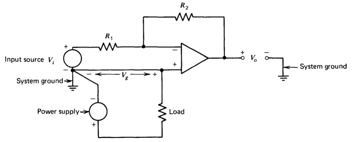
One frequent grounding problem stems from voltage drops in ground lines as a consequence of current flow through these lines. Figure 11.9 illustrates an obviously poor configuration. Here both a signal source and a power supply are connected to a single ground point. However, the current through a load is returned to the low side of the power supply via a wire that also sets the potential at the noninverting input of the operational amplifier. If this current creates a potential \(V_g\) at the noninverting input with respect to system ground, the amplifier output voltage with respect to system ground will be
\[V_o = -\dfrac{R_2}{R_1} V_i + \dfrac{R_1 + R_2}{R_1} V_g \nonumber \]
The error term involving current flow through the ground return line can be substantial, since narrow printed-circuit conductors and connector pins can have considerable resistance and inductance.
While the obvious topology illustrated in Figure 11.9 is relatively easy to avoid, somewhat better disguised variations occur with disturbing frequency. The solution is to design the system with two different ground networks. One of these networks, called signal ground, serves as the return for critical points such as signal sources, feedback networks, and precision voltage references. Every attempt is made to keep both a-c and d-c currents in this network small so that it is essentially an equipotential network. High currents from noncritical loads (an excellent example is the logic often found in complex systems that include both analog and digital components) have their own ground-return network called power ground. These two grounds connect at only one point, which is also the low side of all system power supplies.
Selection of Passive Components
The passive components used in conjunction with operational amplifiers must be selected with care to obtain satisfactory performance.
Metal-film or carbon-film resistors with tolerances of 1 % are inexpensive and readily available. These resistors can be obtained with temperature coefficients as low as 25 parts per million per degree Centigrade, and have fair long-term stability. They are acceptable in less demanding applications. We should note, however, that if 1% resistors are used, loop transmissions in excess of 100 are wasted in many connections.
Wire-wound resistors may be used where accuracy, stability, and temperature coefficient are of primary concern, since units are available that can maintain values to within 0.01 %or better with time and over moderate temperature excursions. Disadvantages of these resistors include relatively large size and poor dynamic characteristics because of their distributed nature. It is important to realize that the excellent temperature stability of these resistors can easily be negated if they are combined with components such as potentiometers for trimming. The accepted procedure when adjustments are required is to use shunt or series connections of selectable, stable resistors to closely approximate the required value. A potentiometer with a total range of a fraction of a percent of the desired value can then be used to complete the trim. The temperature coefficient of the relatively less stable element has little effect since the potentiometer resistance is a very small fraction of the total.
At least one manufacturer offers precision relatively thick metal-film resistors with tolerances to 0.005 %. While the long-term stability and temperature coefficient of these units is not as good as that of the best wire wounds, their small size and excellent dynamic characteristics recommend them in many demanding applications.
The selection of acceptable capacitors is even more difficult. In addition to tolerance and stability problems, capacitors exhibit the phenomenon of dielectric absorption.One manifestation of this effect is that capacitors tend to "remember" and creep back toward the prior voltage if open circuited following a step voltage change. The time required to complete this transient ranges from milliseconds to thousands of seconds, while its magnitude can range from a fraction of a percent to as much as 25 % of the original change, depending primarily on the capacitor dielectric material. Dielectric absorption deteriorates the performance of any circuit using capacitors, with sample and holds (where step voltage changes are routine) and integrators being particularly vulnerable.
Teflon and polystyrene are the best dielectric materials from the point of view of dielectric absorption. The dielectric-absorption coefficient (roughly equal to the fractional recovery following a step voltage change) can be less than 0.1 % for capacitors properly constructed from these materials. They also have very high resistivity so that self-time constants (the product of capacitance and the shunt resistance that results from dielectric or case resistivity) in excess of 106 seconds are possible. While the temperature coefficient for either of these materials is normally the order of 100 parts per million per degree Centigrade, special processing or combinations of capacitors with two types of dielectrics can lower temperature coefficient to a few parts per million per degree Centigrade. The primary disadvantages are relatively large size and high cost (particularly for teflon) and a maximum temperature of \(85^{\circ} C\) for polystyrene.
Mica or glass capacitors often provide acceptable characteristics for lower-value units. Polycarbonate has considerably better volumetric efficiency than either teflon or polystyrene, and is used for moderate- and large-value capacitors. Dielectric absorption is somewhat poorer, but still acceptable in many applications. Mylar-dielectric capacitors are inexpensive and have an absorption coefficient of approximately 1%. These units are often used in noncritical applications.
Ceramic capacitors, particularly those constructed using high-dielectric constant materials, have a particularly unfortunate combination of characteristics for most operational-amplifier circuits, and should generally be avoided except as decoupling components or in other locations where dielectric absorption is unimportant.