
5.2: Series Compensation
- Page ID
- 58450

One way to change the performance of a feedback system is to alter the transfer function of either its forward-gain path or its feedback path. This technique of modifying a series element in a single-loop system is called series compensation. The changes may involve the d-c gain of an element or its dynamics or both.
Adjusting the D-C Gain
One conceptually straightforward modification that can be made to the loop transmission is to vary its d-c or midband value \(a_0f_0\). This modification has a direct effect on low-frequency desensitivity, since we have seen that the attenuation to changes in forward-path gain provided by feedback is equal to \(1 + a_0f_0\).
The closed-loop dynamics are also dependent on the magnitude of the low-frequency loop transmission. The example involving Figure 4.6 showed how root-locus methods are used to determine the relationship between \(a_0f_0\) and the damping ratio of a dominant pole pair. A second approach to the control of closed-loop dynamics by adjusting \(a_0f_0\) for a specific value of \(M_p\) was used in the example involving Figure 4.24.
An assumption common to both of these previous examples was that the value of \(a_0f_0\) could be selected without altering the singularities included in the loop transmission. For certain types of feedback systems independence of the d-c magnitude and the dynamics of the loop transmission is realistic. The dynamics of servomechanisms, for example, are generally dominated by mechanical components with bandwidths of less than 100 Hz. A portion of the d-c loop transmission of a servomechanism is often provided by an electronic amplifier, and these amplifiers can provide frequency-independent gain into the high kilohertz or megahertz range. Changing the amplifier gain changes the value of \(a_0f_0\) but leaves the dynamics associated with the loop transmission virtually unaltered.
This type of independence is frequently absent in operational amplifiers. In order to increase gain, stages may have to be added, producing significant changes in dynamics. Lowering the gain of an amplifying stage may also change dynamics because, for example, of a relationship between the input capacitance and voltage gain of a common-emitter amplifier. A further practical difficulty arises in that there is generally no predictable way to change the d-c open-loop gain of available discrete- or integrated-circuit operational amplifiers from the available terminals.
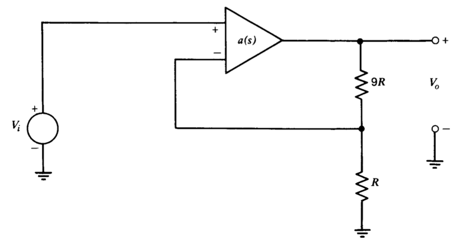
An alternative approach involves modification of the d-c loop trans mission by means of the feedback network connected around the amplifier. The connection of Figure 5.1\(a\) illustrates one possibility. The block diagram for this amplifier, assuming negligible loading at either input or output, is shown in part b of this figure, while the block diagram after reduction to unity-feedback form is shown in part \(c\). If the shunt resistance \(R\) from the inverting input to ground is an open circuit, the d-c value of the loop transmission is completely determined by \(a_0\) and the ideal closed-loop gain \(-R_2/R_1\). However, inclusion of \(R\) provides an additional degree of freedom so that the d-c loop transmission and the ideal gain can be changed independently.
This technique is illustrated for a unity-gain inverter (\(R_1 = R_2\)) and
\[a(s) = \dfrac{10^6}{(s +1)(10^{-5} s + 1)} \nonumber \]
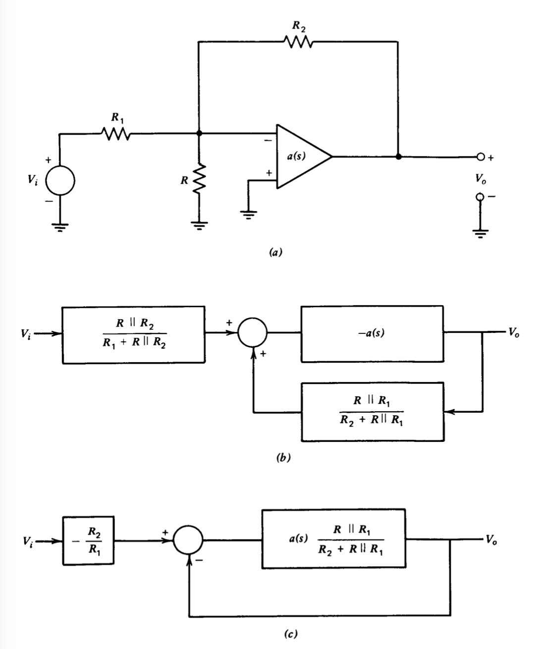
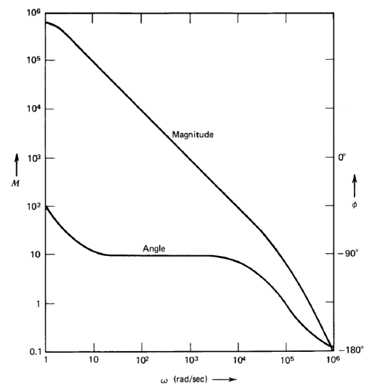
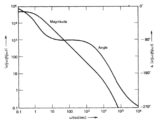
A Bode plot of this transfer function is shown in Figure 5.2. If \(R\) is an open circuit, the magnitude of the loop transmission is one at approximately \(2.15 \times 10^5\) radians per second, since the magnitude of \(a(s)\) at this frequency is equal to the factor of two attenuation provided by the \(R_1-R_2\) network. The phase margin of the system is \(25^{\circ}\), and Figure 4.26\(a\) shows that the closed-loop damping ratio is 0.22. Since Figure 4.26 was generated assuming this type of loop transmission, it yields exact results in this case. If the resistor \(R\) is made equal to \(0.2R_1\), the loop-transmission unity-gain frequency is lowered to \(10^5\) radians per second by the factor-of-seven attenuation provided by the network, and phase margin and damping ratio are increased to \(45^{\circ}\) and 0.42, respectively. One penalty paid for this type of attenuation at the input terminals of the amplifier is that the voltage offset and noise at the output of the amplifier are increased for a given offset and noise at the amplifier input terminals (see Problem P5.2).
Creating a Dominant Pole
Elementary considerations show that a single-pole loop transmission results in a stable system for any amount of negative feedback, and that the closed-loop bandwidth of such a system increases with increasing \(a_0f_0\). Similarly, if the loop transmission in the vicinity of the unity-gain frequency is dominated by one pole, ample phase margin is easily obtained. Because of the ease of stabilizing approximately single-pole systems, many types of compensation essentially reduce to making one pole dominate the loop transmission.
One brute-force method for making one pole dominate the loop trans mission of an amplifier is simply to connect a capacitor from a node in the signal path to ground. If a large enough capacitor is used, the gain of the amplifier will drop below one at a frequency where other amplifier poles can be ignored. The obvious disadvantage of this approach to compensation is that it may drastically reduce the closed-loop bandwidth of the system.
A feedback system designed to hold the value of its output constant independent of disturbances is called a regulator.Since the output need not track a rapidly varying input, closed-loop bandwidth is an unimportant parameter. If a dominant pole is included in the output portion of a regulator, the low-pass characteristics of this pole may actually improve system performance by attenuating disturbances even in the absence of feedback.
One possible type of voltage regulator is shown in simplified form in Figure 5.3. An operational amplifier is used to compare the output voltage with a fixed reference. The operational amplifier drives a series regulator stage that consists of a transistor with an emitter resistor. The series regulator isolates the output of the circuit from an unregulated source of voltage. The load includes a parallel resistor-capacitor combination and a disturbing current source. The current source is included for purposes of analysis and will be used to determine the degree to which the circuit rejects load-current changes. The dominant pole in the system is assumed to occur because of the load, and it is further assumed that the operational amplifier and series transistor contribute no dynamics at frequencies where the loop- transmission magnitude exceeds one.
The block diagram of Figure 5.3\(b\) models the regulator if it is assumed that the common-base current gain of the transistor is one and that the resistor \(R\) is large compared to the reciprocal of the transistor transconductance. This diagram verifies the single-pole nature of the system loop transmission.
As mentioned earlier, the objective of the circuitry is to minimize changes in load voltage that result from changes in the disturbing current and the unregulated voltage. The disturbance-to-output closed-loop transfer functions that indicate how well the regulator achieves this objective are
\[\dfrac{V_l}{I_d} = \dfrac{R/a_0}{RC_L s/a_0 + (1 + R/a_0 R_L)} \nonumber \]
and
\[\dfrac{V_l}{V_u} = \dfrac{1/a_0}{RC_L s/a_0 + (1 + R/a_0 R_L)} \nonumber \]
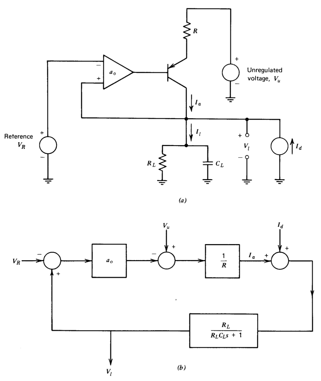
If sinusoidal disturbances are considered, the magnitude of either disturbance-to-output transfer function is a maximum at d-c, and decreases with increasing frequency because of the low-pass characteristics of the load. Increasing \(C_L\) improves performance, since it lowers the frequency at which the disturbance is attenuated significantly compared to its d-c value. If it is assumed that arbitrary loads can be connected to the regulator (which is the usual situation, if, for example, this circuit is used as a laboratory power supply), the values of \(R_L\) and \(C_L\) must be considered variable. The minimum value of \(C_L\) can be constrained by including a capacitor with the regulation circuitry. The load-capacitor value increases as external loads are connected to the regulator because of the decoupling capacitors usually associated with these loads. Similarly, \(R_L\) decreases with increasing load to some minimum value determined by loading limitations.
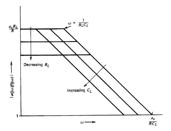
The compensation provided by the pole at the output of the regulator maintains stability as \(R_L\) and CL change, as illustrated in the Bode plot of Figure 5.4. (The negative of the loop transmission for this plot is \(a_0R_L/ R(R_LC_Ls + 1)\), determined directly from Figure 5.3\(b\).) Note that the unity-gain frequency can be limited by constraining the maximum value of the \(a_0/RC_L\) ratio, and thus crossover can be forced before other system elements affect dynamics. The phase margin of the system remains close to \(90^{\circ}\) as \(R_L\) and \(C_L\) vary over wide limits.
Lead and Lag Compensation
If the designer is free to modify the dynamics of the loop transmission as well as its low-frequency magnitude, he has considerably more control over the closed-loop performance of the system. The rather simple modification of making a single pole dominate has already been discussed.
The types of changes that can be made to the dynamics of the loop transmission are constrained, even in purely mathematical systems. It is tempting to think that systems could be improved, for example, by adding positive phase shift to the loop transmission without changing its magnitude characteristics. This modification would clearly improve the phase margin of a system. Unfortunately, the magnitude and angle characteristics of physically realizable transfer functions are not independent, and transfer functions that provide positive phase shift also have a magnitude that increases with increasing frequency. The magnitude increase may result in a higher system crossover frequency, and the additional negative phase shift that results from other elements in the loop may negate hoped-for advantages.
The way that series compensation is implemented and the types of compensating transfer functions that can be obtained in practical systems are even further constrained by the hardware realities of the feedback system being compensated. The designer of a servomechanism normally has a wide variety of compensating transfer functions available to him, since the electrical networks and amplifiers usually used to compensate servomech anisms have virtually unlimited bandwidth relative to the mechanical portions of the system. Conversely, we should remember that the choices of the feedback-amplifier designer are more restricted because the ways that the transfer function of an amplifier can be changed, particularly near its unity-gain frequency where transistor bandwidth limitations dominate performance, are often severely constrained.
Two distinct types of transfer functions are normally used for the series compensation of feedback systems, and these types can either be used separately or can be combined in one system. A lead transfer function can be realized with the network shown in Figure 5.5. The transfer function of this network is
\[\dfrac{V_o (s)}{V_i (s)} = \dfrac{1}{\alpha} \left [\dfrac{\alpha \tau s + 1}{\tau s + 1} \right ] \nonumber \]
where \(\alpha = (R_1 + R_2)/R_2\) and \(\tau = (R_1 || R_2)C\). As the name implies, this network provides positive or leading phase shift of the output signal relative to the input signal at all frequencies. Lead-network parameters are usually selected to locate its singularities near the crossover frequency of the system being compensated. The positive phase shift of the network then improves the phase margin of the system. In many cases, the lead network has negligible effect on the magnitude characteristics of the compensated system at or below the crossover frequency, since we shall see that a lead network provides substantial phase shift before its magnitude increases significantly.
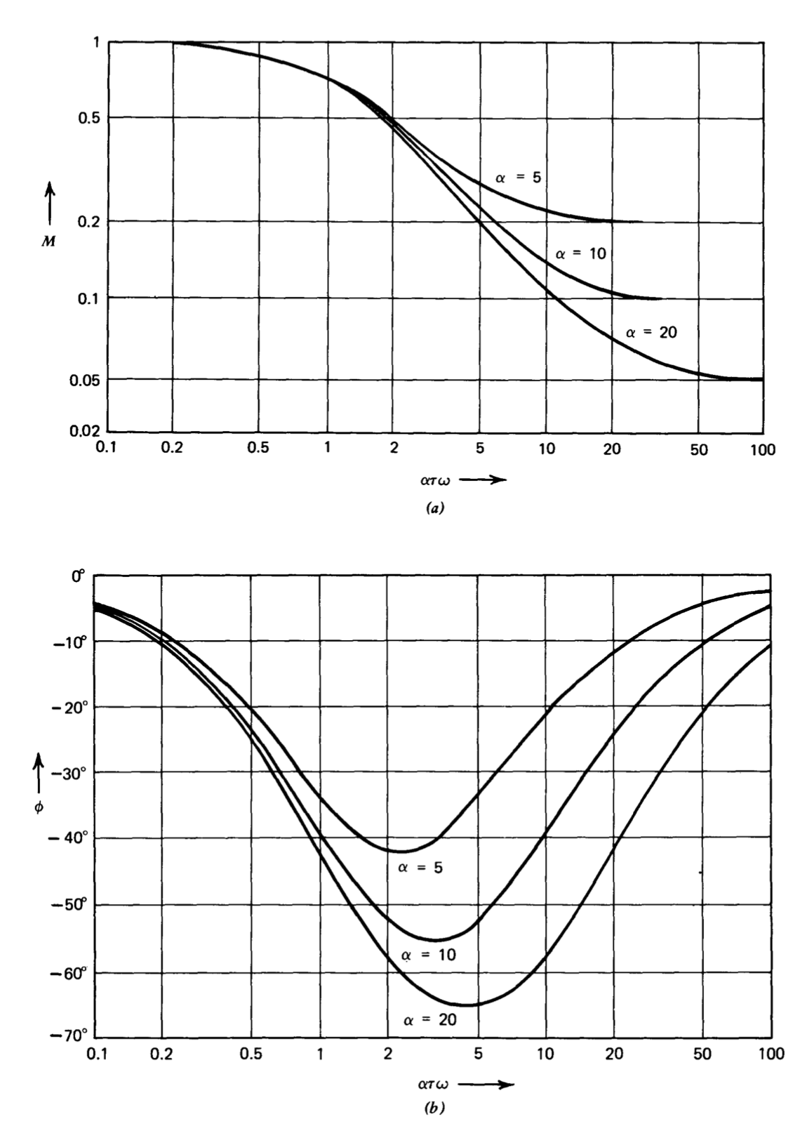
The lag network shown in Figure 5.6 has the transfer function
\[\dfrac{V_o (s)}{V_i (s)} = \dfrac{\tau s + 1}{\alpha \tau s + 1} \nonumber \]
where \(\alpha = (R_1 + R_2)/R_2\) and \(\tau = R_2 C\). The singularities of this type of network are usually located well below crossover in order to reduce the crossover frequency of a system so that the negative phase shift associated with other elements in the system is reduced at the unity-gain frequency. This effect is possible because of the attenuation of the lag network at frequencies above both its singularities.
The maximum magnitude of the phase angle associated with either of these transfer functions is
\[\phi_{\max} = \sin^{-1} \left [\dfrac{\alpha - 1}{\alpha + 1} \right ] \nonumber \]
and this magnitude occurs at the geometric mean of the frequencies of the two singularities. The gain of either network at its maximum-phase-shift frequency is \(1/\sqrt{a}\).
The magnitudes and angles of lead transfer functions for \(\alpha\) values of 5, 10, and 20, are shown in Bode-plot form in Figure 5.7. Figure 5.8 shows corresponding curves for lag transfer functions. The corner frequencies for
the poles of the plotted functions are normalized to one in these figures. As mentioned earlier, an important feature of the lead transfer function is that it provides substantial positive phase shift over a range of frequencies
below its zero location without a significant increase in magnitude. The reason stems from a basic property of real-axis singularities. At frequencies below the zero location, this singularity dominates the lead transfer function, so
\[\dfrac{V_o (s)}{V_i (s)} \simeq \dfrac{1}{\alpha} (\alpha \tau s + 1) \nonumber \]
The magnitude and angle of this function are
\[M = \dfrac{1}{\alpha} [\sqrt{1 + (\alpha \tau \omega)^2}] \nonumber \]
\[\phi = \tan^{-1} \alpha \tau \omega \nonumber \]
At a small fraction of the zero location, \(\alpha \tau \omega \ll 1\), so
\[M \simeq \dfrac{1}{\alpha} \left [1 + \dfrac{(\alpha \tau \omega)^2}{2} \right ] \nonumber \]
\[\phi \simeq \alpha \tau \omega \nonumber \]
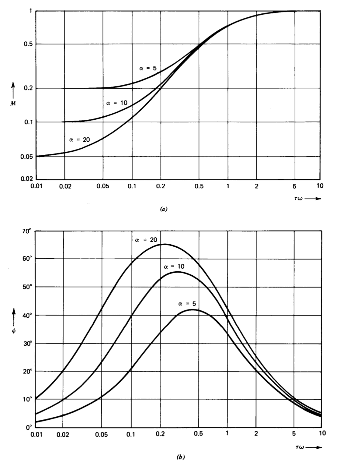
Since the angle increases linearly with frequency in this region while the magnitude increases quadratically, the angle change is relatively larger at a given frequency. The same sort of reasoning applies even if the zero is located at or slightly below crossover. Figure 5.7 shows that the positive phase shift of a lead transfer function with a reasonable value of \(\alpha\) is approximately \(40^{\circ}\) at its zero location, while the magnitude increase is only a factor of 1.4. Much of this advantage is lost at frequencies beyond the geometric mean of the singularities, since the positive phase shift decreases beyond this frequency, while the magnitude continues to increase.
We should recognize that an isolated zero can be used in place of a lead transfer function, and that this type of transfer function actually has phase-shift characteristics superior to those of the zero-pole pair. However, the unlimited high-frequency gain implied by an isolated zero is clearly unachievable, at least at sufficiently high frequencies. Thus the form of the lead transfer function introduced earlier reflects the realities of physical systems.
The important feature of the lag transfer function illustrated in Figure 5.8 is that at frequencies well above the zero location, it provides a magnitude attenuation equal to the ratio of the two singularity locations and negligible phase shift. It can thus be used to reduce the magnitude of the loop trans mission without significantly adding to the negative phase shift of this transmission at moderate frequencies.
Example
Lead and lag networks were originally developed for use in servomech anisms, and provide a powerful means for compensation when their singularities can be located arbitrarily with respect to other system poles and when independent adjustment of the low-frequency loop-transmission magnitude is possible. Even without this flexibility, which is usually absent with operational-amplifier circuits, lead or lag compensation can provide effective control of closed-loop performance in certain configurations. As an example, consider the noninverting gain-of-ten amplifier connection shown in Figure 5.9. It is assumed that the input admittance and output impedance of the operational amplifier are small. The open-loop transfer function of the operational amplifier is(While an analytic expression is used for \(a(s)\) in this example, the reader should realize that the open-loop transfer function of an operational amplifier will generally not be available in this form. Note, however, that an experimentally determined Bode plot is completely acceptable for all of the required manipulations, and that this information can always be determined. The general characteristics of the assumed open-loop transfer function are typical of many operational amplifiers, in that this quantity is dominated by a single pole at low frequencies. At frequencies closer to the unity-gain frequency, additional negative phase shift results from effects related to transistor limitations. As we shall see in later sections, these effects constrain the ultimate performance capabilities of the amplifier.)
\[a(s) = \dfrac{5 \times 10^5}{(s + 1)(10^{-4} s + 1) (10^{-5} s + 1)} \nonumber \]
and it is assumed that the user cannot alter this function. When connected as shown in Figure 5.9 the value of \(f\) is 0.1, and thus the negative of the loop transmission is
\[a(s)f(s) = \dfrac{5 \times 10^4}{(s + 1)(10^{-4} s + 1) (10^{-5} s + 1)}\label{eq5.2.11} \]
The closed-loop gain is
\[\begin{array} {rcl} {\dfrac{V_o (s)}{V_i (s)} = A(s)} & = & {\dfrac{a(s)}{1 + a(s) f(s)}} \\ {} & \simeq & {\dfrac{10}{2 \times 10^{-14} s^3 + 2.2 \times 10^{-9} s^2 + 2 \times 10^{-5} s + 1}} \end{array} \nonumber \]
A Bode plot of Equation \(\ref{eq5.2.11}\) (Figure 5.10) shows that the system crossover frequency is \(2.1 \times 10^4\) radians per second, its phase margin is \(13^{\circ}\), and the gain margin is 2.
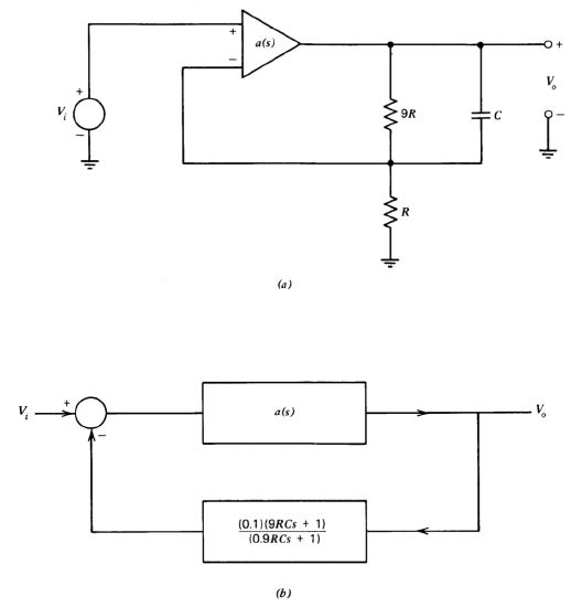
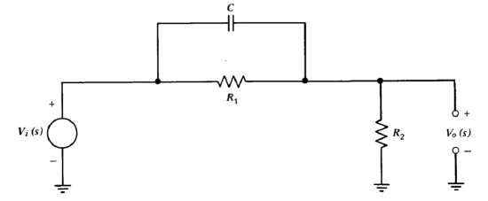
While the problem statement precludes altering \(a(s)\), we can introduce a lead transfer function into the loop transmission by including a capacitor across the upper resistor in the feedback network. The topology is shown in Figure 5.11\(a\), with a block diagram shown in Figure 5.11\(b\). The negative of the loop transmission for the system is
\[a'(s) f'(s) = \dfrac{5 \times 10^4 (9RCs + 1)}{(s + 1)(10^{-4}s + 1)(10^{-5} s + 1)(0.9 RCs + 1)}\label{eq5.2.13} \]
Several considerations influence the selection of the \(R-C\) product that locates the singularities of the lead network. As mentioned earlier, the objective of a lead network is to provide positive phase shift in the vicinity of the crossover frequency, and maximum positive phase shift from the network results if crossover occurs at the geometric mean of the zero-pole pair. However, the network singularities and the crossover frequently cannot be adjusted independently for this system, since if the zero of the lead network is located at a frequency below about \(3 \times 10^4\) radians per second, the crossover frequency increases. An increase in crossover frequency increases the negative phase shift of the amplifier at this frequency, offsetting in part the positive phase shift of the network. A related consideration involves the effect of the lead network on the ideal closed-loop gain of the amplifier since the network is introduced in the feedback path and the ideal gain is reciprocally related to the feedback transfer function. If the lead-network zero is located at a low frequency, a low-frequency closed-loop pole that reduces the closed-loop bandwidth of the system results.
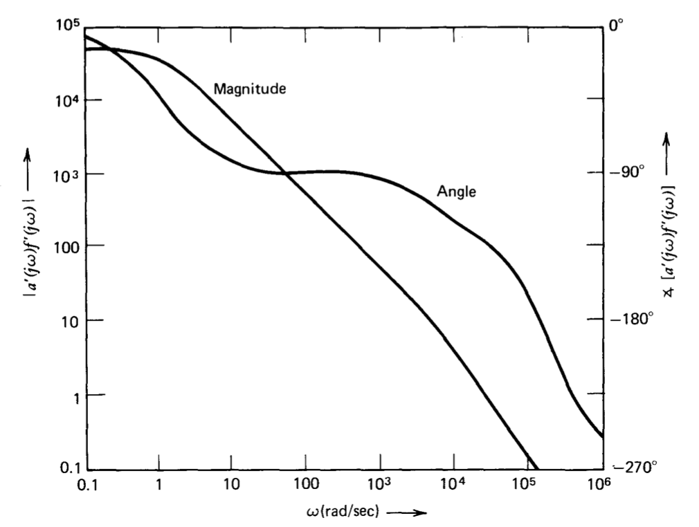
A reasonable compromise in this case is to locate the zero of the lead network near the unity-gain frequency, in an attempt to obtain positive phase shift from the network without a significant increase in the crossover frequency. The choice \(RC = 4.44 \times 10^{-6}\) seconds locates the zero at \(2.5 \times 10^4\) radians per second. A Bode plot of Equation \(\ref{eq5.2.13}\) for this value of RC is shown in Figure 5.12. The unity-gain frequency is increased slightly to \(2.5 \times 10^4\) radians per second, while the phase margin is increased to the respectable value of \(47^{\circ}\). Gain margin is 14.
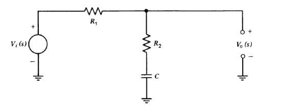
A lag transfer function can be introduced into the forward path of the amplifier by shunting a series resistor-capacitor network between its input terminals as shown in Figure 5.13\(a\). Note that the same loop transmission could be obtained by shunting the R-valued resistor with the \(R_1 -C\) network, since both the bottom end of the \(R\)-valued resistor and the noninverting input of the amplifier are connected to incrementally grounded points. If this later option were used, the \(R_1-C\) network would introduce the lag transfer function into the feedback path of the topology. Consequently, the ideal closed-loop transfer function would include the reciprocal of the lag function. Since the singularities of lag networks are generally located at low frequencies, the closed-loop transfer function could be adversely influenced at frequencies of interest. (See Problem P5.7.)
The system block diagram for the topology of Figure 5.13\(a\) is shown in Figure 5.13\(b\). In this case, the lag transfer function appears in both the feedback path and a forward path outside the loop. The block diagram can be rearranged as shown in Figure 5.13\(c\); and this final diagram shows that including the \(R_1-C\) network between amplifier inputs leaves the ideal closed- loop gain unchanged. The negative of the loop transmission for Figure 5.13\(c\) is
\[a''(s) f''(s) = 0.1 \dfrac{(\tau s + 1)}{(\alpha \tau s + 1)} a(s) \nonumber \]
where
\[\alpha = \dfrac{R_1 + 0.9 R}{R_1} \text{ and } \tau = R_1 C\nonumber \]
As mentioned earlier, the singularities of a lag transfer function are generally located well below the system crossover frequency so that the lag network does not deteriorate phase margin significantly. A frequently used rule of thumb suggests locating the zero of the lag network at one-tenth of the crossover frequency that results following compensation, since this value yields a maximum negative phase contribution of \(5.7^{\circ}\) from the network at crossover. We also, rather arbitrarily, decide to choose the lag-network parameters to yield a phase margin of approximately \(47^{\circ}\), the same value as that of the system compensated with a lead network. The Bode plot of the system without compensation, Figure 5.10, aids in selecting lag-network parameters. This plot indicates an uncompensated phase angle of \(-128^{\circ}\) and an uncompensated magnitude of 6.2 at a frequency of \(6.7 \times 10^3\) radians per second. If the value of 6.2 is the chosen high-frequency attenuation a of the lag network, the compensated crossover frequency will be \(6.7 \times 10^3\) radians per second. The \(5^{\circ}\) of negative phase shift anticipated from a properly located lag network combines with the \(- 128^{\circ}\) of phase shift of the system prior to compensation to yield a compensated phase margin of \(47^{\circ}\). The zero of the lag network is located at \(6.7 \times 10^2\) radians per second, a factor 10 below crossover. These design objectives are met with \(R_1 = 0.173R\) and \(R_1C = 1.5 \times 10^{-3}\) seconds. With these values, the negative of the loop transmission is
\[a''(s) f''(s) = \dfrac{5 \times 10^4 (1.5 \times 10^{-3} s + 1)}{(s + 1)(10^{-4} s + 1)(10^{-5} s + 1)(9.3 \times 10^{-3} s + 1)} \nonumber \]
This transfer function, plotted in Figure 5.14, indicates predicted values for crossover frequency and phase margin. The gain margin is 15.
Two other modifications of the loop transmission result in Bode plots that are similar to that of the lag-compensated system in the vicinity of the crossover frequency. One possibility is to lower the value of \(a_0f_0\) by a factor of 6.2 (see Section 5.2.1). The required reduction can be accomplished by simply using the shunt-resistor value determined for lag compensation directly across the input terminals of the operational amplifier. This modification results in the same crossover frequency as that of the lag-compen sated amplifier, and has several degrees more phase margin since it does not have the slight negative phase shift associated with the lag network at crossover. Unfortunately, the lowered \(a_0f_0\) results in a lower value for desensitivity compared with that of the lag-compensated amplifier at all frequencies below the zero of the network.
A second possibility is to move the lowest-frequency pole of the loop transmission back by a factor of 6.2. This modification might be made to the amplifier itself, or could be accomplished by appropriate selection of lag-network components. The effect on parameters in the vicinity of crossover is essentially identical to that of reducing \(a_0f_0\). Desensitivity is retained at d-c with this method, but is lowered at intermediate frequencies compared to that provided by lag compensation. These two approaches to compensating the amplifier described here are investigated in detail in Problem P5.8.
The discussion of series compensation up to this point has focused on the use of the frequency-domain concepts of phase margin, gain margin, and crossover frequency to determine compensating-network parameters. Root-locus methods cannot be used directly since the value of \(a_0f_0\) is not varied to effect compensation. However, the root-locus sketches for the uncompensated, lead-compensated, and lag-compensated systems shown in Figure 5.15 do lend a degree of insight into system behavior. (There is significant distortion in these sketches, since it is not convenient to present sketches accurately where the singularities are located several decades apart.)
The root-locus diagram of Figure 5.15\(a\) illustrates the change in closed-loop pole location as a function of \(a_0f_0\) for the uncompensated system. Adding the lead network (Figure 5.15\(b\)) shifts the dominant branches to the left and, thus, improves the damping ratio of this pair of poles for a given value of \(a_0f_0\).
The effect of lag compensation is somewhat more subtle. The root-locus diagram of Figure 5.15\(c\) is virtually identical to that of Figure 5.15\(a\) except in the immediate vicinity of the lag-network singularity pair. However, a gain calculation using rule 8 (Section 4.3.1) shows that the value of \(a_0f_0\) required to reach a given damping ratio for the dominant pair is higher by approximately a factor of a when the lag network is included.
Root contours can also be used to show the effects of varying a single parameter of either the lead or the lag network. This design approach is explored in Problems P5.9 and P5.10.
Evaluation of the Effects of Compensation
There are several ways to demonstrate the improvement in performance provided by compensation. Since the parameters of the compensating transfer function are usually determined with the aid of loop-transmission Bode plots, one simple way to evaluate various types of compensation is to compare the desensitivity obtained from them. The considerations used to determine lead- and lag-compensation parameters for an operational amplifier connected to provide a gain of 10 were described in detail in Section 5.2.4. The resulting loop transmissions, repeated here for convenience, are
\[a'(s) f'(s) = \dfrac{5 \times 10^4 (4 \times 10^{-5} s + 1)}{(s + 1)(10^{-4} s + 1)(10^{-5} s + 1)(4 \times 10^{-6} s + 1)}\label{eq5.2.16} \]
and
\[a''(s) f''(s) = \dfrac{5 \times 10^4 (1.5 \times 10^{-3} s + 1)}{(s + 1)(10^{-4} s + 1)(10^{-5} s + 1)(9.3 \times 10^{-3} s + 1)}\label{eq5.2.17} \]
for the lead- and lag-compensated cases, respectively. The phase-margin obtained by either method is approximately \(47^{\circ}\).
It was mentioned that the stability of the uncompensated amplifier could be improved by either lowering \(a_0f_0\) by a factor of 6.2, resulting in
\[a''' (s) f(s)''' = \dfrac{8.1 \times 10^3}{(s + 1)(10^{-4} s + 1)(10^{-5} s + 1)} \nonumber \]
or by lowering the location of the first pole by the same factor, yielding
\[a'''' (s) f''''(s) = \dfrac{5 \times 10^4}{(6.2 s + 1)(10^{-4} s + 1)(10^{-5} s + 1)} \nonumber \]
Either of these approaches results in a crossover frequency identical to that of the lag-compensated system and a phase margin of approximately \(52^{\circ}\).
The magnitude portions of the loop transmissions for these four cases are compared in Figure 5.16. The relative desensitivities that are achieved at various frequencies, as well as the relative crossover frequencies, are evident in this figure.
An alternative way to evaluate various compensation techniques is to compare the error coefficients that are obtained using them. This approach is explored in Problem P5.11. As expected, systems with greater desensitivity generally also have smaller-magnitude error coefficients.
The discussion of compensation up to now has focused on the use of Bode plots, since this is usually the quickest way to find compensating parameters. However, design objectives are frequently stated in terms of transient response, and the inexperienced designer often feels an act of faith is required to accept the principle that systems with properly chosen values for phase margin, gain margin, and crossover frequency will produce satisfactory transient responses. The step responses shown in Figure 5.17 are offered as an aid to establishing this necessary faith.
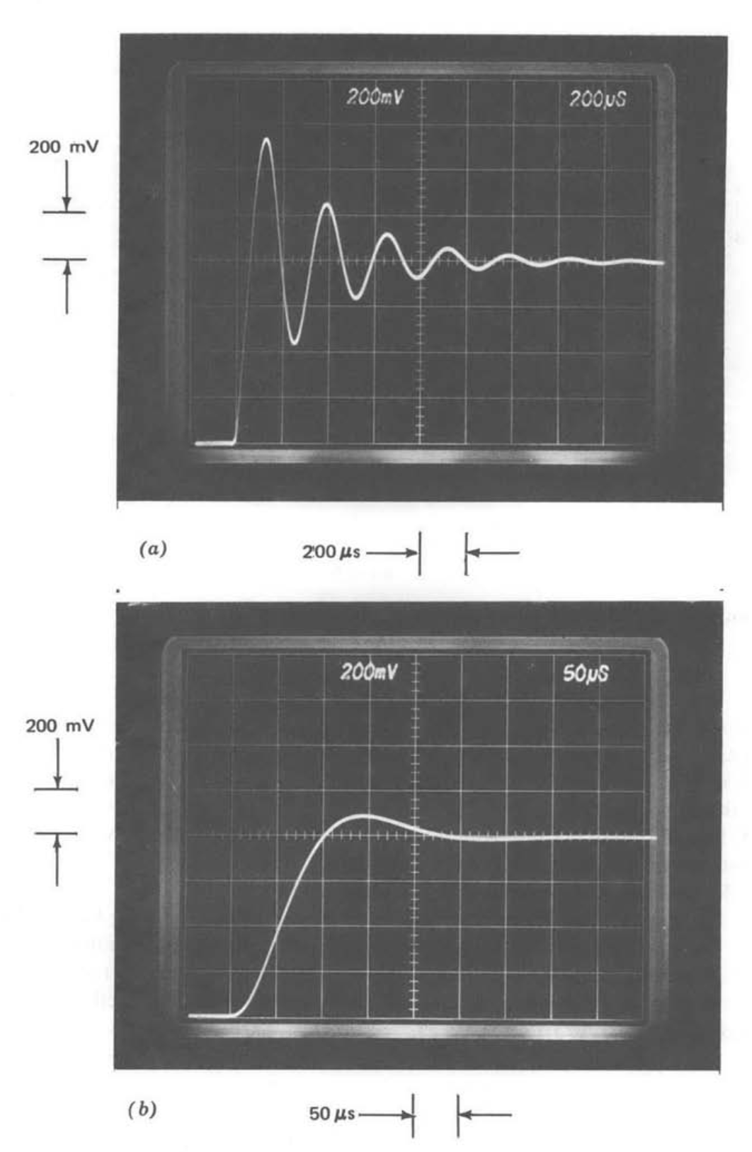
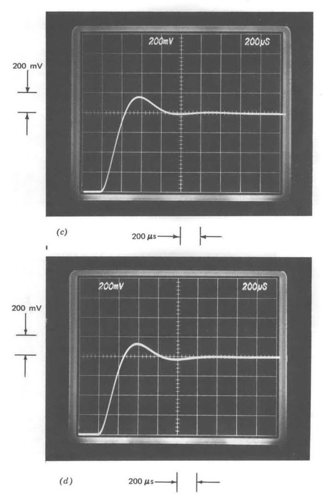
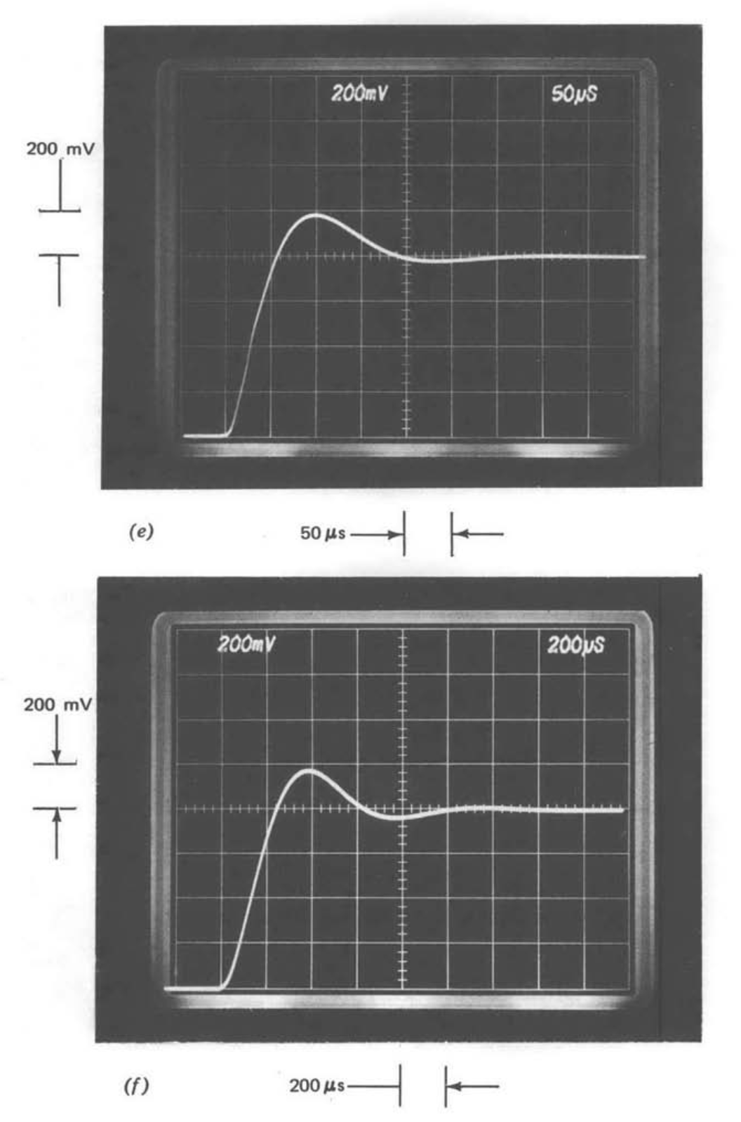
Figure 5.17 Response of gain-of-ten amplifier to an 80-mV step. (\(a\)) No compensation. (\(b\)) Lead compensated. (\(c\)) Lag compensated. (\(d\)) Lowered \(a_0 f_0\). (\(e\)) Lead compensation in forward path. (\(f\)) Second-order approximation to (\(c\)).
Figure 5.17\(a\) shows the step response of the gain-of-ten amplifier without compensation. The large peak overshoot and poor damping of the ringing reflect the low phase margin of the system. The overshoot and damping for the lead compensated, lag compensated, and reduced \(a_0f_0\) cases (Figs. 5.17\(b\), 5.17\(c\), and 5.17\(d\), respectively) are significantly improved, as anticipated in view of the much higher phase margins of these connections. The step response obtained by lowering the frequency of the first pole in the loop is not shown, since it is indistinguishable from Figure 5.17\(d\).
Certain features of these step responses are evident from the figures. The peak overshoot exhibited by the amplifier with reduced \(a_0f_0\) is slightly less than that of the amplifier with lag compensation, reflecting slightly higher phase margin. Similarly, the rise time of lag-compensated amplifier is very slightly faster, again reflecting the influence of relative phase margin on the performance of these two systems with identical crossover frequencies. The smaller peak overshoot of the lead-compensated system does not imply greater relative stability for this amplifier, but rather occurs because of the influence of the lead network in the feedback path on the ideal closed-loop gain.
Figure 5.17\(e\) shows the step response that results if lead compensation is provided in the forward path rather than in the feedback path. Thus the loop transmission for this transient response is identical to that of Figure 5.17\(b\) (Equation \(\ref{eq5.2.16}\)), but the feedback path for the system illustrated in Figure 5.17\(e\) is frequency independent. While forward-path lead compensation was prohibited by the problem statement of the earlier examples, Figure 5.17\(e\) provides a more realistic indication of relative stability than does Figure 5.17\(b\), since Figure 5.17\(e\) is obtained from a system with a frequency-independent ideal gain. The difference between these two systems with identical loop transmissions arises because of differences in the closed-loop zero locations (see Section 4.3.4).
The peak overshoot and relative damping of Figs. 5.17\(c\) and 5.17\(e\) are virtually identical, demonstrating that, at least for this example, equal values of phase margin result in equal relative stability for the lead- and lag-compensated systems. The rise time of Figure 5.17\(e\) is approximately one-quarter that of Figure 5.17\(c\), and this ratio is virtually identical to the ratio of the crossover frequencies of the two amplifiers.
The step response of Figure 5.17\(f\) is that of a second-order system with \(\zeta = 0.45\) and \(\omega_n = 8.5 \times 10^3\) radians per second. These values were obtained using Figure 4.26\(a\) to determine a second-order approximating system to the lag-compensated amplifier. The similarity of Figs. 5.17\(c\) and 5.17\(f\) is another example of the accuracy that is frequently obtained when complex systems are approximated by first- or second-order ones. The loop transmission for the lag-compensated system (Equation \(\ref{eq5.2.17}\)) includes four poles and one zero. However, this quantity has only a single-pole roll off between \(6.7 \times 10^2\) radians per second and the crossover frequency, with a second pole in the vicinity of crossover. It can thus be well approximated as a system with two widely separated poles, the model from which Figure 4.26 was developed.
Related Considerations
Several additional comments concerning the relative benefits of different series compensation methods are in order. The evaluation of performance in the previous example seems to imply advantages for lead compensation. The lead-compensated amplifier appears superior if desensitivity at various frequencies, error-coefficient magnitude, or speed of transient response is
used as the indicator of performance. Furthermore, if the lead transfer function is included in the feedback path, the amplifier exhibits better- damped transient responses than can be obtained from other types of compensation selected to yield equivalent phase margin. The advantages associated with lead compensation primarily reflect the higher value for cross over frequency and the correspondingly higher closed-loop bandwidth that is frequently possible with this method. It should be emphasized, however, that bandwidth in excess of requirements usually deteriorates overall performance. Larger bandwidth increases the noise susceptibility of an amplifier and frequently leads to greater stability problems because of stray inductance or capacitance.
Lead compensation usually aggravates the stability problem if the loop also includes elements that provide large negative phase shift over a wide frequency range without a corresponding magnitude attenuation. (While the constraints of physical realizability preclude elements that provide positive phase shift without an amplitude increase, the less useful converse described above occurs with distressing frequency.) For example, consider a system that combines a frequency-independent gain in a loop with a \(\tau\)-second time delay such as that provided by a delay line. The negative of the loop transmission for this system is
\[a(s) f(s) = a_0 e^{-s \tau} \nonumber \]
The time delay is an element that has a gain magnitude of one at all frequencies and a negative phase shift that is linearly related to frequency. The Nyquist diagram (Figure 5.18) for this system shows that it is unstable for \(a_0 > 1\). The use of lead compensation compounds the problem, since the positive phase shift of the lead network cannot counteract the unlimited negative phase shift of the time delay, while the magnitude increase of the lead function further lowers the maximum low frequency desensitivity consistent with stable operation.
The correct approach is to use a dominant pole to decrease the magnitude of the loop transmission before the phase shift of time delay becomes excessive. The limiting case of an integrator (pole at the origin) works well, and this modification results in
\[a(s) f(s) = \dfrac{a_0}{s} e^{-s \tau} \nonumber \]
The desensitivity of this function is infinite at d-c. The reader should convince himself that the system is absolutely stable for any positive value of \(a_0 < \pi / 2\tau\), and that at least \(45^{\circ}\) of phase margin is obtained with positive \(a_0 < \pi /4\tau\).
The use of lag compensation introduces a type of error that compromises its value in some applications. If the step response of a lag-compensated amplifier is examined in sufficient detail, it is often found to include a long time-constant, small-amplitude "tail," which may increase inordinately the time required to settle to a small fraction of final value. Similarly, while the error coefficient ei may be quite small, the time required for the ramp error to reach its steady-state value may seem incompatible with the amplifier crossover frequency.
As an aid to understanding this problem, consider a system with \(f(s) = 1\) and
\[a(s) = \dfrac{1000 (0.1 s + 1)}{s (s + 1)}\label{eq5.2.24} \]
This transfer function is an idealized representation of a system that combines a single dominant pole with lag compensation to improve desensitivity. The zero of the lag network is located a factor of 10 below the cross over frequency. The closed-loop transfer function is
\[A(s) = \dfrac{a(s)}{1 + a(s)f(s)} = \dfrac{(0.1s + 1)}{10^{-3} s^2 + 0.101s + 1} = \dfrac{(0.1s + 1)}{(0.09s + 1)(0.011s + 1)} \nonumber \]
The response of this system to a unit step is easily evaluated via Laplace techniques, with the result
\[v_o (t) = 1 - 1.126 e^{-t/0.011} + 0.126 e^{-t/0.09}\label{eq5.2.26} \]
This step response reaches 10% of final value in 0.02 second, a reasonable value in view of the 100 radian per second crossover frequency of the system. However, the time required to reach 1% of final value is 0.23 second because of the final term in Equation \(\ref{eq5.2.26}\). Note that if \(a(s)\) is changed to \(100/s\), a transfer function with the same unity-gain frequency as Equation \(\ref{eq5.2.24}\) and less gain magnitude at all frequencies below 10 radians per second, the time required for the system step response to reach 1% of final value is approximately 0.05 second.
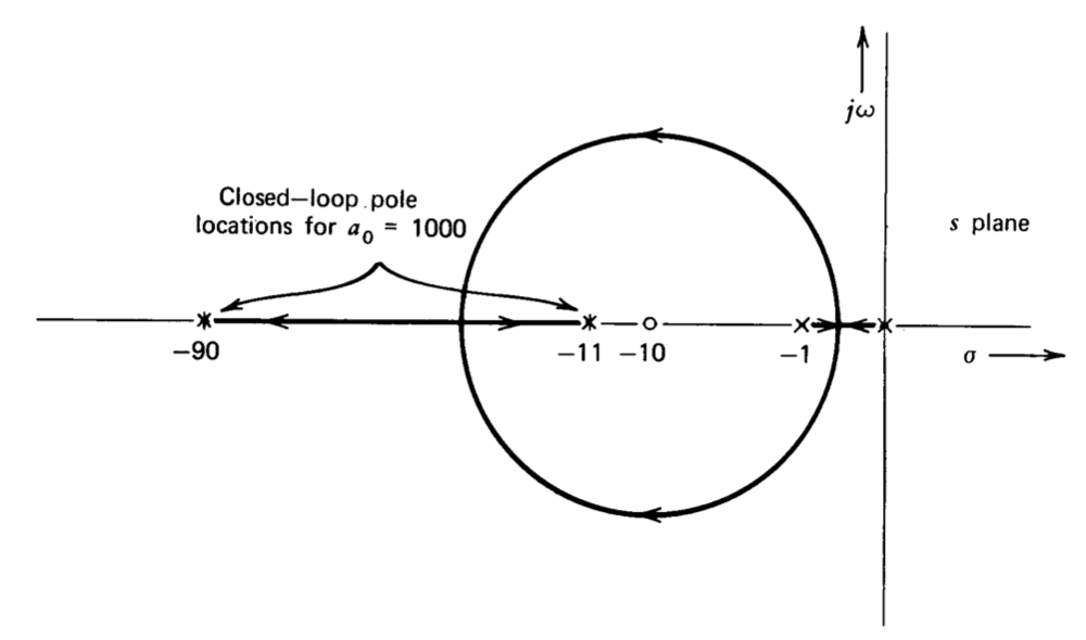
The root-locus diagram for the system (Figure 5.19) clarifies the situation. The system has a closed-loop zero with a corner frequency at 10 radians per second since the zero shown in the diagram is a forward-path singularity. The feedback forces one closed-loop pole close to this zero. The resultant closely spaced pole-zero doublet adds a long-time-constant tail to the otherwise well-behaved system transient response. The reader should recall that it is precisely this type of doublet that deteriorates the step response of a poorly compensated oscilloscope probe. Since linear system relationships require that the ramp response be the integral of the step response, the time required for the ramp error to reach final value is similarly delayed.
Similar calculations show that as the lag transfer function is moved further below crossover, the amplitude of the tail decreases, but its time constant increases. We conclude that while lag compensation is a powerful technique for improving desensitivity, it must be used with care when the time required for the step response to settle to a small fraction of its final value or the time required for the ramp error to reach final value is constrained.
It should be emphasized that a closed-loop pole will generally be located close to any open-loop zero with a break frequency below the crossover frequency. Thus the type of tail associated with lag compensation can also result with, for example, lead compensation that often includes a zero below crossover. The performance difference results because the zero and the closed-loop pole that approaches it to form a doublet are usually located close to the crossover frequency for lead compensation. Thus the decay time of the resultant tail, which is determined by the closed-loop pole in question, does not greatly lengthen the settling time of the system.
Table 5.1 Comparison of Series-Compensating Methods
| Type | Special Considerations | Advantages | Disadvantages |
| Reduced \(a_0 f_0\) | Simplicity | Lowest desensitivity. | |
| Create dominant pole | Lower the frequency of the existing dominant pole if possible. Locate at the output of a regulator. |
Can improve poise immunity of system. Usually the type of choise for a regulator. | Lowers bandwidth. |
| Lag | Locate well below crossover frequency. | Better desensitivity than either of above. | May add undesirable "tail" to transient response. |
| Lead | Locate zero near crossover frequency. | Greatest densensitivity. Lowest error coefficients. Fastest transient response. |
Increases sensitivity to noise. Cannot be used with fixed elements that contribute excessive negative phase shift. |
It is difficult to develop generalized rules concerning compensation, since the proper approach is highly dependent on the fixed elements included in the loop, on the types of inputs anticipated, on the performance criterion chosen, and on numerous other factors. In spite of this reservation, Table 5.1 is an attempt to summarize the most important features of the four types of series compensation described in this section.