
7.4: INPUT CURRENT
- Page ID
- 69436

The discussion of input-circuit errors up to this point has focused on voltage drift referred to the input. Additional input offset signals arise from input current if the signal source resistance is high. In many d-c amplifiers constructed using bipolar transistors, offsets from input current dominate. One alternative is the use ofjunction-gate or metal-oxide-semiconductor (Mos) field-effect transistors that exhibit substantially lower input currents. Unfortunately, the voltage drift of junction-gate field-effect transistors is about one order of magnitude worse than that of bipolar devices. Mos devices, with threshold voltages dependent on trapped surface charge, are even more unstable. The techniques used to stabilize the operation of these devices are significantly different than those used with bipolar transistors and are not discussed here.(L. Orchard and T. Hallen, "Fet Amplifier Design Precautions," EDN, August, 1968. )
In contrast to the base-to-emitter voltage, which varies in a highly predictable fashion with temperature, the temperature dependence of base current is a complex function of transistor structure. Furthermore, matching most parameters of two transistors, including 0 at one temperature, does not insure equal current gain at some different temperature. As a matter of practical interest, the fractional change in current gain with temperature, \((1/\beta )(\partial \beta /\partial T)\), is typically 0.5 to 1% per degree Centigrade, with somewhat higher values measured at low collector currents and low temperatures.
While these unpredictable variations in \(\beta\) make input-current compensation schemes less precise than voltage-drift compensation, several useful methods are available for lowering input current.
Operation at Low Current
In spite of manufacturers' reluctance to admit it, there are many types of transistors that exhibit useful current gains at low collector currents. It is not unusual to find units with a value for \(\beta\) in excess of 10 at \(I_c = 10^{-11} A\), and devices with current gains of 100 at \(I_c = 10^{-9} A\) are easily selected from several families. Clearly, operation at reduced collector current is one approach to low input current. A disadvantage of this technique is that collector-to-base leakage current may dominate input current, particularly at high temperatures, or may contribute to excessive voltage drift (see Section 7.3.5). However, \(I_{CBO}\) can be eliminated by operating a transistor at zero collector-to-base voltage, and there are several circuit techniques that keep this voltage low yet permit operation over a wide range of input voltages.
A more fundamental problem is the low \(f_T\) (current gain-bandwidth product) of devices operating at low collector currents. Below some current level the base-to-emitter capacitance \(C_{\pi}\) is dominated by a space-chargelayer capacitance, and this quantity is independent of current. Since collector-to-base capacitance \(C_{\mu}\) is independent of operating current and \(g_m\) is directly proportional to current,
\[f_T = \dfrac{g_m}{2\pi (C_{\pi} + C_{\mu})} \nonumber \]
is directly proportional to current at low operating currents. A typical value for \(f_T\) at a collector current of 1 nA is 1 kHz.
Cancellation Techniques
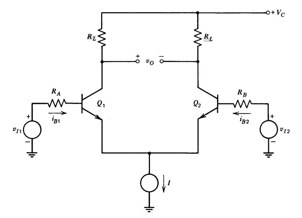
While the variation of input current with temperature is not as predictable as that of the base-to-emitter voltage, several compensation techniques take advantage of matching this quantity. Figure 7.13 shows one possibility. Here it is assumed that the source impedances associated with the two input signals are resistive and fixed. If
\[i_{B1} R_A = i_{B2} R_B\label{eq7.4.2} \]
the drop across each source resistor is equal and the net effect is simply to apply a common-mode input signal to the amplifier.(It is assumed in this discussion that the input currents are independent of differential input voltage. This is not true for large signals, but in many applications the signals applied to a differential amplifier are sufficiently small to make base-current variations with signal level negligible. A technique to compensate for varying input current with signal levels is indicated in Section 7.4.3.) Similarly, if
\[R_A \dfrac{\partial i_{B1}}{\partial T} = R_B \dfrac{\partial i_{B2}}{\partial T}\label{eq7.4.3} \]
the effects of temperature-dependent input currents are eliminated. Both Equations \(\ref{eq7.4.2}\) and \(\ref{eq7.4.3}\) are satisfied if the resistors are selected to equalize voltage drops at one temperature and if the fractional change in \(\beta\) with temperature is equal for both devices. The technique of equalizing the resistances connected to the two inputs (effectively assuming equal input currents) is frequently used in operational-amplifier connections.
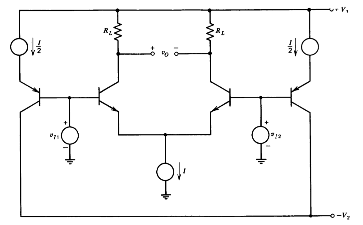
In some applications, it is important to reduce the magnitude of one or both base currents of an amplifier, not simply insure that the two input currents to a differential amplifier are equal. Clearly one very simple approach is to provide the amplifier bias currents via resistors connected to an appropriate-polarity supply voltage. Unfortunately, the bias current supplied by this method is temperature independent, and thus the variation in amplifier input current with temperature is not decreased. Figure 7.14 shows one way to provide a degree of cancellation. If the \(\beta\)'s of corresponding NPN and PNP transistors are equal, the current seen at either input is zero when the collector currents of the two NPN's are equal. The use of current sources in the emitters of the PNP's provides a compensating current that is independent of common-mode level.
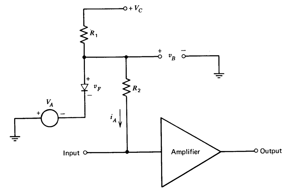
Another technique is to use the temperature-dependent forward-voltage characteristics of a diode to generate a temperature-dependent compen sating current, as shown in Figure 7.15. The amplifier itself is shown diagrammatically in this figure, and only one input, close to ground potential, is indicated. Resistor \(R_1\) establishes a bias current through the diode. It is assumed that this current is constant since it is selected to be much larger than \(i_A\) and that \(V_C\) is much greater than \(V_A\) and \(v_F\). The temperature dependence of \v_F\), \(\partial v_F/\partial T\),is identical to that of a transistor (Equation 7.2.5) and is approximately constant with temperature.(Carrier recombination in a diode can multiply the \(3k/q\) term in Equation 7.2.5 by a factor between one and two. This modification does not significantly alter the basic dependence.) The compensating current \(i_A\) is equal to \(v_B/R_2\), and has a fractional change with temperature equal to
\[\dfrac{1}{i_A} \dfrac{\partial i_A}{\partial T} = \dfrac{1}{v_B} \dfrac{\partial v_B}{\partial T} = \dfrac{1}{(v_F + V_A)} \dfrac{\partial v_F}{\partial T} \nonumber \]
The two degrees of freedom represented by the selection of \(V_A\) and \(R_2\) can be used to cancel at one temperature both the input current and its first derivative with respect to temperature.
There are several variations on this basic topology that effectively bootstrap the reference voltage for the compensating diode from a node referenced to the common-mode input level such as the emitter connection of differential pair. The compensating current provided can be made relatively independent of common-mode level in this way, thus allowing the technique to be used with input voltages at arbitrary levels with respect to ground.
Compensation for Infinite Input Resistance
The compensation methods introduced up to this point have been intended to compensate for temperature variations of the input-transistor bias current. It has been assumed that the input signals are small enough so that the input-current component attributable to the input resistance of the amplifier is negligible. While this inequality is generally satisfied in applications (such as operational amplifiers) where the input circuit is followed by additional stages of voltage amplification, many differential-amplifier stages operate with appreciable differential signals applied to their input.
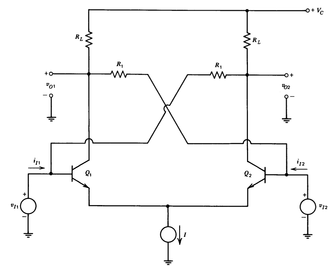
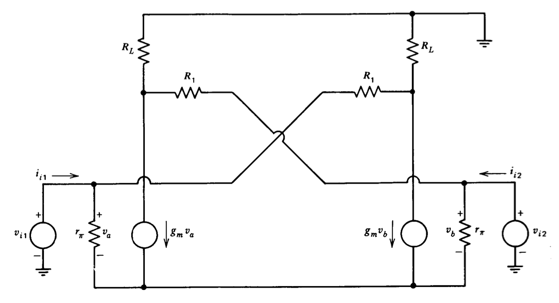
Figure 7.16 shows a connection that can be adjusted to provide infinite input resistance to differential signals. Consider a differential input signal, \(v_{I1} = - v_{I2}\). A positive \(v_{I1}\) increases the current flowing into the base of \(Q_1\) and causes a positive change in \(v_{O2}\). By proper choice of parameters it is possible to supply the required base current through the right-hand \(R_1\) so that the change in ii, is zero(This technique, which involves positive feedback, is not without its hazards. The topology of the circuit is essentially identical to that of a flip-flop, and if the circuit is overcompensated and driven from high impedance sources, bistable operation is possible.). The necessary value for \(R_1\) is computed with the aid of the incremental model of Figure 7.17. (The usual approximations have been included in developing the model.) Normally \(R_1 \gg R_L\) so that the loading by \(R_1\) can be neglected. With this assumption, the incremental input current \(i_{i1}\), that results for a pure differential input is
\[i_{i1} = v_{i1} \left [\dfrac{1}{r_{\pi}} - \left (\dfrac{g_m R_L - 1}{R_1} \right ) \right ] \nonumber \]
If the voltage gain of the circuit is large so that \(g_mR_L \gg 1\), the differential input resistance is infinite for
\[\dfrac{g_m r_{\pi} R_L}{R_1} = 1 \ \ \text{ or } \ R_1 = \beta R_L \nonumber \]
The common-mode input resistance is lowered by the compensating resistors, since Figure 7.17 shows that
\[\dfrac{v_{i1}}{i_{i1}} |_{v_{i1} = v_{i2}} = R_1 \nonumber \]
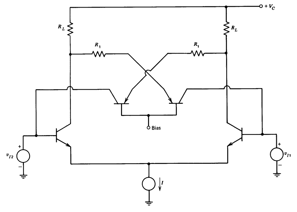
High common-mode input resistance can be restored by including PNP transistors in this compensating circuit as shown in Figure 7.18. In addition to supplying the compensating current from a high-resistance source, selection of the bias voltage gives an additional degree of freedom in controlling the quiescent level of the compensating current.
Darlington Input
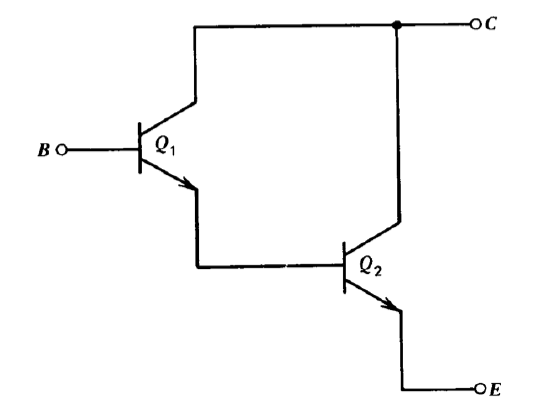
One obvious way to lower input current is to use transistors with higher current gains. As mentioned earlier, transistors with current gains in excess of 1000 are available, and this value should increase as processing techniques improve. It is also possible to use two transistors in the Darlington connection shown in Figure 7.19. It is easy to show that at low frequencies this connection approximates a single transistor between terminals \(B, C\), and \(E\) with current gain given by
\[\beta = \beta_2 (\beta_1 + 1) + \beta_1 \simeq \beta_1 \beta_2 \nonumber \]
and a transconductance
\[g_m = \dfrac{q}{2kT} I_C \nonumber \]
Current gains in excess of 101 are possible with available devices.
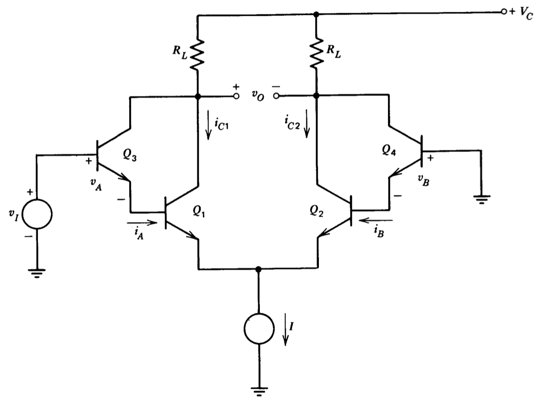
Figure 7.20 shows a differential amplifier with Darlington-connected input transistors. While a connection of this type yields low values for input current, the voltage drift for this configuration usually exceeds that of the conventional differential amplifier. The problem stems from differential changes in the base currents of transistors \(Q_1\) and \(Q_2\). (Remember that current gain varies in a relatively unpredictable way with temperature.) Since
the resistance seen at the emitters of transistors \(Q_3\) and \(Q_4\) is relatively high, current changes produce significant changes in voltages \(v_A\) and \(v_B\). A differential change in \(v_A\) and \(v_B\) results in drift equal in value to this change.
In order to compute drift referred to the input from this effect, it is necessary to determine how \(v_I\) must vary with \(i_A\) and \(i_B\) to keep \(v_O = 0\). Assume the operating point values for the two emitter currents are \(I_A\) and \(I_B\). The incremental changes in these two currents that arise from changes in the current gains of transistors \(Q_1\) and \(Q_2\) are related to \(I_A\) and \(I_B\) by
\[i_a = -I_A \dfrac{\Delta \beta_1}{\beta_1} \nonumber \]
\[i_b = -I_B \dfrac{\Delta \beta_2}{\beta_2} \nonumber \]
where \(\Delta \beta /\beta\) is recognized as the fractional change in current gain for a transistor.
The incremental output resistance of an emitter follower is approximately equal to the reciprocal of its transconductance. Thus the incremental differential change between \(v_A\) and \(v_B\) caused by changes in \(i_A\) and \(i_B\), which is identically equal to the change in \(v_I\) required to keep \(v_O\) equal to zero is
\[v_a - v_b = \dfrac{i_a}{g_{m3}} - \dfrac{i_b}{g_{m4}} = \dfrac{I_B \Delta \beta_2}{g_{m4} \beta_2} - \dfrac{I_A \Delta \beta_1}{g_{m3} \beta_1}\label{eq7.4.11} \]
Since the transconductances are proportional to operating-point cur rents, Equation \(\ref{eq7.4.11}\) reduces to
\[v_a - v_b = \dfrac{I_B \Delta \beta_2}{(qI_B/kT)\beta_2} - \dfrac{I_A \Delta \beta_1}{(qI_A/kT)\beta_1} = \dfrac{kT}{q} \left (\dfrac{\Delta \beta_2}{\beta_2} - \dfrac{\Delta \beta_1}{\beta_1}\right ) \nonumber \]
Note that the drift component attributable to this effect is dependent only on the differential changes in the fractional current gains of the inner transistors. A typical value for the fractional change in current gain with temperature is 0.6% per degree Centigrade. If transistors Q, and Q2 have this value matched to within 10%,(This degree of match is realistic for discrete transistors selected for matched base-to emitter voltages and current gains. Better results are normally achieved with monolithic matched transistors where the manufacuring process for the two devices is highly uni form.) the resultant drift is 15 \(\mu V/ ^{\circ} C\).
Another potential difficulty with the use of the Darlington input connections is that its fractional change in input current with temperature is approximately a factor of two greater than that of an individual transistor because two devices are cascaded in the Darlington connection. Thus the low bias current of the Darlington configuration does not result in correspondingly low changes in bias current with temperature.
It is possible to trade input current for drift by increasing the emitter currents of \(Q_3\) and \(Q_4\) above the base currents of \(Q_1\) and \(Q_2\), for example by placing resistors from base to emitter of \(Q_1\) and \(Q_2\). Changes in base current have less effect since the output resistances of \(Q_3\) and \(Q_4\) are lower as a consequence of increased bias current. This technique is frequently used in the design of amplifiers with Darlington input transistors.