
9.2: ANALYSIS
- Page ID
- 58466

In order to demonstrate the performance features of the amplifier introduced in the previous section, it is necessary to approximate analytically some of its more important characteristics. While the exact details of the analysis are specific to this amplifier, several significant features, particularly those concerning dynamics and compensation, are common to all two-stage operational amplifiers. Thus the conclusions we shall reach extend beyond this particular circuit.
We should realize that certain aspects of the following analysis are likely to be in error by a factor of two or more, since the uncertainty of some of the parameter values associated with the transistors limits accuracy. Another type of difficulty is encountered in the analysis of the dynamics of the amplifier, since a number of poles are predicted in the vicinity of the \(f_T\) of the transistors used in the amplifier. Such results are always suspect because transistor-model deficiencies prevent accurate analysis in this frequency range. Fortunately, these inaccuracies are of little concern since our objective is not so much precise prediction of the performance of this particular amplifier as it is an understanding of the important features of this general type of amplifier.
Low-Frequency Gain
One important characteristic of an operational amplifier is its d-c open-loop gain. Calculation of the gain of this amplifier is necessary because accurate measurement of the signal levels that would permit experimental gain determination is precluded by noise and drift.
By far the largest fraction of the low-frequency gain of the amplifier occurs in the cascode stage for this particular implementation of the basic topology. The analysis of the complete amplifier is facilitated by initially developing a low-frequency equivalent circuit for the cascode amplifier. The analysis of Section 8.3.4 showed that the voltage gain of an unloaded cascode amplifier is
\[-\dfrac{\beta_6}{2 \eta_6} = -\dfrac{g_{m6} r_{\mu 6}}{2}\nonumber \]
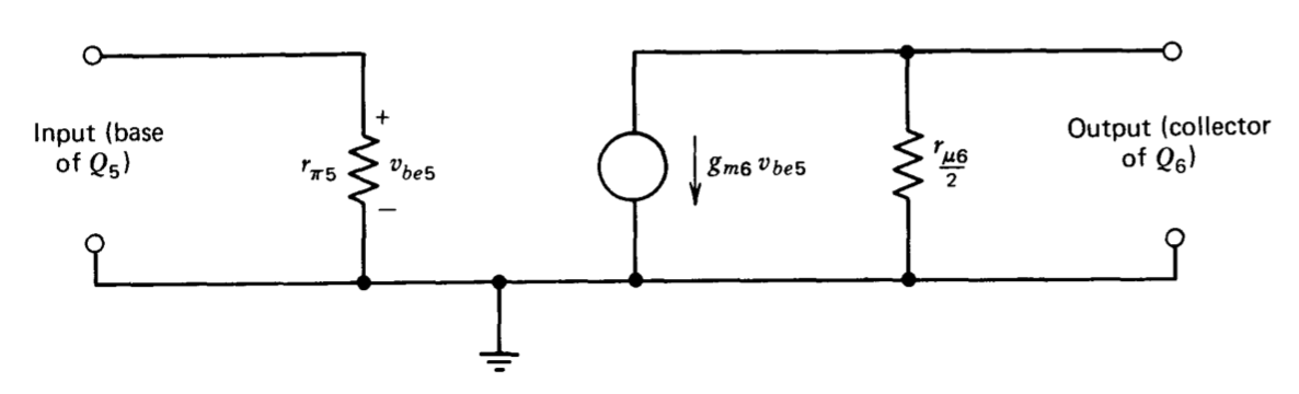
while its input resistance is \(r_{\pi 5}\). (Subscripts differentiating between the two transistors in the cascode connection refer to Figure 9.1.) While the output resistance of the cascode connection was not specifically calculated, a result from Section 8.3.5 can be used to determine this quantity. Equation 8.3.47 gives \(r_{\mu} /2\) as the output resistance of a common-base current source with a large incremental emitter-circuit resistance. The output resistance of the cascode must be identical since its output consists of a common-base connection with a large emitter-circuit resistance. These results show that the low-frequency performance of the cascode portion of the amplifier can be modeled by the equivalent circuit of Figure 9.2.
The d-c gain of the circuit shown in Figure 9.1 is determined using the parameter values shown in Table 9.1 for the transistors. The calculation is performed assuming that the noninverting input of the amplifier is incrementally grounded. This assumption yields the same value for d-c gain that would be obtained considering a true differential input voltage. Incrementally grounding the noninverting input does eliminate an insignificant high-frequency term in the transfer function that results from signals fed through the collector-to-base capacitance of \(Q_2\) (see Section 8.2.3).
Table 9.1 Transistor Parameters for Circuit of Figure 9.1
| Transistor Number |
Type | \(I_C\) or \(I_D\) (\(\mu A\)) |
\(g_m\) (mmho) |
\(\beta\) | \(r_{\pi}\) (\(k\Omega\)) |
\(r_{\mu}\) (\(k\Omega\)) |
\(r_{o}\) (\(k\Omega\)) |
\(C_{\mu}\) or \(C_{gd}\) (pF) |
\(C_{\pi}\) or \(C_{gs}\) (pF) |
| \(Q_1, Q_2\) | 2N5963 | 10 | 0.4 | 1100 | 2750 | * | * | 6 | 10 |
| \(Q_3\) | 2N3707 | 20 | * | * | * | * | * | 8 | 10 |
| \(Q_4, Q_5, Q_6\) | 2N4250 | 50 | 2 | 350 | 175 | 500 | 1.4 | 10 | 15 |
| \(Q_7\) | 2N3707 | 50 | 2 | 200 | 100 | 500 | 2.5 | 8 | 10 |
| \(Q_8\) | TIS58 | 2 mA | * | - | - | - | - | 2 | * |
| \(Q_9\) | 2N3707 | 2 mA | * | * | * | * | * | * | * |
| \(Q_{10}\) | 2N2219 | * | * | 200 | * | * | * | * | * |
| \(Q_{11}\) | 2N2905 | * | * | 200 | * | * | * | * | * |
| \(Q_{12}\) | 2N3707 | 0 | * | * | * | * | * | * | * |
| \(Q_{13}\) | 2N4250 | 0 | * | * | * | * | * | * | * |
- Not relevant.
* Value unimportant in included analysis.
Overall gain is found by first calculating the transfer relationships for various portions of the circuit. An incremental input voltage applied to the base of \(Q_1\), \(v_i\), causes a change in the collector current of \(Q_2\) given by
\[i_{c2} = -\dfrac{v_i g_{m1}}{2}\label{eq9.2.1} \]
(It has been assumed that both input transistors are operating at equal currents so that \(g_{m1} = g_{m2}\).)
The previously developed cascode equivalent circuit shows that the change in base voltage of \(Q_5\) is related to the \(Q_2\) collector-current change by
\[v_{be5} = -i_{c2} (325 k\Omega || r_{\pi 5})\label{eq9.2.2} \]
(The collector-circuit potentiometer has been assumed set to center position so that the load resistor of transistor \(Q_2\) is equal to \(325\ k\Omega\).) In order to determine the voltage gain of the cascode amplifier, it is necessary to calculate the load applied to it. The input resistance of field-effect transistor \(Q_8\) is essentially infinite, while the output resistance for the current source \(Q_7\) is
\[r_{\mu 7} \left | \right | \left [\dfrac{1 + g_{m7} (r_{\pi 7} || 68 k \Omega)}{g_{o7}} \right ] \nonumber \]
(See Equation 8.3.45.) It is computationally convenient to reduce this equation now and to introduce the experimentally verifiable assumption that \(r_{\mu 7} \simeq r_{\mu 6}\). This value is reasonable, since both devices are operating at identical currents, and are fabricated using similar (though complementary) process ing. The 2N3707 has a typical \(\beta\) of 200 at \(50\ \mu A\), so that \(r_{\pi 7}\) is typically \(100\ k\Omega\) at this current. Therefore, \(r_{\pi 7} || 68 k\Omega \simeq 0.4r_{\pi 7}\). Accordingly, the output resistance of \(Q_7\) becomes
\[r_{\mu 7} \left | \right | \left [\dfrac{1 + g_{m7} (0.4 r_{\pi 7})}{g_{o7}} \simeq r_{\mu 7} \left | \right | \left [ \dfrac{0.4 \beta_7}{g_{o7}} \right ] = r_{\mu 7} || 0.4 r_{\mu 7} \simeq 0.28 r_{\mu 7} \right ]\label{eq9.2.4} \]
Using this relationship, the assumed equivalence of \(r_{\mu 7}\) and \(r_{\mu 6}\), and the model of Figure 9.2 shows that the loaded cascode voltage gain is
\[\dfrac{v_{cb6}}{v_{be5}} \simeq -g_{m6} \left (\dfrac{r_{\mu 6}}{2} || 0.28 r_{\mu 6} \right ) \simeq -g_{m6} (0.18 r_{\mu 6} )\label{eq9.2.5} \]
Recognizing that the unloaded voltage gain from the collector of \(Q_6\) to the amplifier output is unity and combining Equations \(\ref{eq9.2.1}\), \(\ref{eq9.2.2}\), and \(\ref{eq9.2.5}\) yields
\[\dfrac{v_o}{v_i} = -\dfrac{g_{m1}}{2} (325 k\Omega || r_{\pi 5}) g_{m6} (0.18 r_{\mu 6}) \label{eq9.2.6} \]
Substituting parameter values from Table 9.1 into Equation \(\ref{eq9.2.6}\) predicts a d-c open-loop gain magnitude of \(4 \times 10^6\). The gain is dominated by the contribution of \(1.8 \times 10^5\) from the cascode amplifier (see Equation \(\ref{eq9.2.5}\)).
Transfer Function
The locations of all poles and zeros of the amplifier could be predicted for the complete circuit by substituting appropriate incremental models for the active devices, although this would be a formidable task even with the aid of a computer. The approach used here is to make relatively crude approximations to gain insight into the controlling dynamics of the amplifier and then to verify the approximate results with a more detailed (though still incomplete) computer analysis.
The unloaded low-frequency voltage gain of the buffer amplifier (transistors \(Q_8\) through \(Q_{11}\)) is unity. Amplifier loads as low as several hundred ohms do not appreciably alter its performance. If the load applied to the amplifier is not capacitive, the frequency response of the buffer approaches the \(f_T\) of the devices used in it. Furthermore, the input impedance of \(Q_8\), which loads the cascode amplifier, is independent of any load applied to the amplifier output since the FET is unilateral. Thus the influence of the buffer can be modeled by simply using the input capacitance of \(Q_8, C_{gd8}\), as a load for the cascode. Similarly, the loading of transistor \(Q_7\) can be represented as a parallel impedance consisting of its output capacitance \(C_{\mu 7}\) and output resistance 0.28\(r_{\mu 7}\) (Equation \(\ref{eq9.2.4}\)).
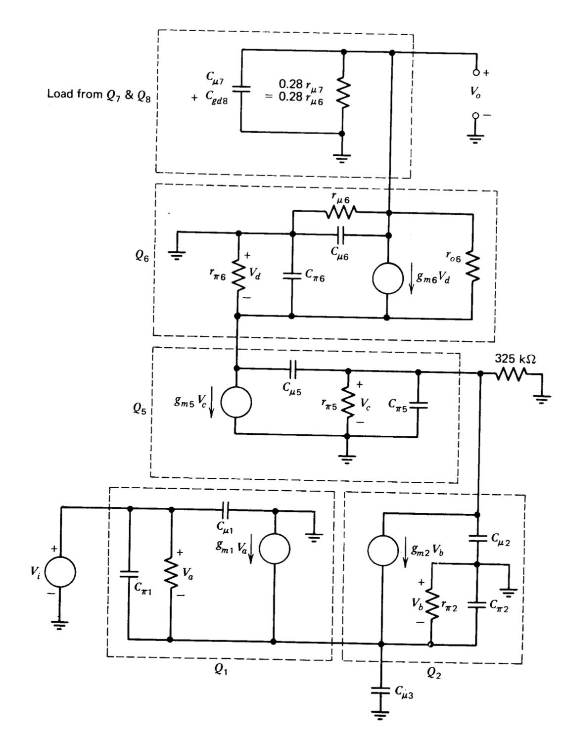
An incremental model that reflects these simplifications is shown in Figure 9.3. The base resistances (\(r_x\)'s) of all transistors, as well as \(r_{\mu}\) and \(r_o\) of transistors other than \(Q_6\) and \(Q_7\) (the transistors in the high-gain portion of the circuit) have also been ignored. An argument based on the concept of open-circuit time constants(See P. E. Gray and C. L. Searle, Electronic Principles: Physics, Models, and Circuits, Wiley, New York, 1969, Chapters 15 and 16. ) is used to further simplify this model. The open-circuit resistances(The open-circuit resistance facing a capacitor is the incremental resistance at the terminal pair in question calculated with all other capacitors in the circuit removed or open-circuited.) facing capacitors \(C_{\pi 1}\), \(C_{\mu 1}\), \(C_{\pi 2}\), \(C_{\mu 3}\), and \(C_{\pi 6}\) are all on the order of \(1/g_m\), for the related transistor or lower. Thus these capacitors do not affect the dynamics of the amplifier at frequencies low compared to the \(f_T\)'s of the various transistors and are eliminated for the initial approximation. As a result of this approximation the only contribution of the input stage to amplifier dynamics is a consequence of the loading \(C_{\mu 2}\) applies to the base of \(Q_5\), and the stage itself can be modeled as a single dependent current source.
The further-simplified incremental model incorporating the approximations introduced above and shown in Figure 9.4 is used to approximate the location of the two low-frequency amplifier poles. The node equations for this circuit are
\[\begin{array} {rcl} {\dfrac{g_{m1} V_i}{2}} & = & {[(C_1 + C_{\mu 5}) s + G_1] V_a - C_{\mu 5} s V_b} \\ {0} & = & {(-C_{\mu 5} s + g_{m5})V_a + (C_{\mu 5} s + g_{m6} + g_{\pi 6} + g_{o 6}) V_b - g_{o6} V_o} \\ {0} & = & {(-g_{m6} - g_{o6})V_b + (C_2 s + g_{o6} + G_2)V_o} \end{array}\label{eq9.2.7} \]
(See Figure 9.4 for the definition of parameters in this equation.)
The poles are found by equating the determinant of the matrix of coefficients of Equation \(\ref{eq9.2.7}\) to zero, yielding
\[\dfrac{C_1C_2C_{\mu 5}}{g_{m6} G_1 (G_2 + g_{\mu 6})} s^3 + \dfrac{C_2(C_1 + 2C_{\mu 5}}{G_1 (G_2 + g_{\mu 6})} s^2 + \dfrac{C_2}{C_2 + g_{\mu 6}} s + 1 = 0\label{eq9.2.8} \]
In reducing Equation \(\ref{eq9.2.7}\) to \(\ref{eq9.2.8}\), small terms have been dropped. However, only terms that are small because of transistor and topological inequalities such as \(g_m \gg g_{\pi} \gg g_o \gg g_{\mu}\), and \(C_2 > C_{\mu 6}\) since one component of \(C_2\) is \(C_{\mu 6}\) have been eliminated. Thus the conclusions that will be drawn from Equation \(\ref{eq9.2.8}\) are applicable to a variety of circuits that share this topology rather than being limited to the specific choice of element values shown in Figure 9.1. Fundamental relationships among parameter values also insure that the three poles represented by \(\ref{eq9.2.8}\) will be real and widely spaced. Consequently, this cubic equation can be easily factored, since
\[(\tau_a s + 1)(\tau_b s + 1) (\tau_c s + 1) \simeq \tau_a \tau_b \tau_c s^3 + \tau_a \tau_b s^2 + \tau_a s + 1 \text{ for } \tau_a \gg \tau_b \gg \tau_c \label{eq9.2.9} \]
Equation \(\ref{eq9.2.9}\) allows us to write Equation \(\ref{eq9.2.8}\) as
\[\left (\dfrac{C_2}{C_2 + g_{\mu 6}} s + 1 \right ) \left (\dfrac{C_1 + 2C_{\mu 5}}{G_1} s + 1 \right ) \left (\dfrac{C_1C_{\mu 5}}{g_{m6} (C_1 + 2C_{\mu 5})} s + 1 \right ) = 0 \nonumber \]
indicating that
\[\begin{array} {rcl} {\tau_a} & = & {\dfrac{C_2}{G_2 + g_{\mu 6}}} \\ {\tau_b} & = & {\dfrac{C_1 + 2C_{\mu 5}}{G_1}} \\ {\tau_c} & = & {\dfrac{C_1 C_{\mu 5}}{g_{m6} (C_1 + 2C_{\mu 5})}} \end{array} \label{eq9.2.11} \]
The physical interpretation of the time constants lends insight into the operation of the circuit. The resistance associated with time constant \(\tau_a\) is simply the incremental resistance from the high resistance node (the collector of \(Q_6\)) to ground. [Recall that \(1/(G_2 + g_{\mu 6}) =0.28r_{\mu 6} || r_{\mu 6} || r_{\mu 6} = 0.18r_{\mu 6}\), the value obtained earlier and used in Equation \(\ref{eq9.2.5}\) for the incremental resistance from this node to ground.] Similarly, capacitance \(C_2 = C_{\mu 6} + C_{\mu 7} + C_{gd8}\) is the capacitance from the high resistance node to ground. Since the capacitance of all amplifier nodes is the same order of magnitude, it is not surprising that the dominant amplifier pole is associated with energy storage at the highest resistance node. Substituting values from Table 9.1 shows that \(\tau_a = 1.8\ ms\), implying that the dominant amplifier open-loop pole is located at \(s = - 550\text{ sec}^{-1}\).
Time constant \(\tau_b\) is associated with the resistance and capacitance from the base of \(Q_5\) to ground. The conductance \(G_1\) in Equation \(\ref{eq9.2.11}\) was defined previously as the conductance from this node to ground. The capacitance consists of the collector-to-base capacitance of \(Q_2\) that shunts this node and the total effective input capacitance (including that attributed to Miller effect) \(Q_5\) would display if this transistor were loaded with a resistive load equal to \(1/g_{m5}\). Note that at frequencies much above \(1/\tau_a\) radians per second, the capacitive loading at the collector of \(Q_6\) has reduced the voltage gain of this transistor; as a result, there is no significant feedback to the emitter of \(Q_6\) through \(r_{o6}\) at these frequencies. Thus transistor \(Q_6\) provides the \(1/g_{m6} = 1/g_{m5}\) load for \(Q_5\). The time constant rb is equal to \(4.5\ \mu s\), implying that the second amplifier pole is located at \(s = -2.2 \times 10^5 \text{ sec}^{-1}\). Time constant \(\tau_c\) corresponds to a frequency that approximates \(f_T\) for the transistors in the circuit, and thus to one of many high-frequency poles that are ignored in the simplified analysis.
Combining the d-c gain (Equation \(\ref{eq9.2.6}\)) with the dynamics predicted above yields
\[\dfrac{V_o (s)}{V_i (s)} = \dfrac{-4 \times 10^6}{(1.8 \times 10^{-3} s + 1)(4.5 \times 10^{-6} s + 1)}\label{eq9.2.12} \]
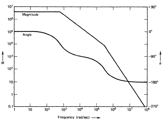
Equation \(\ref{eq9.2.12}\) is shown as a Bode plot(The transfer function plotted in Figure 9.5 is actually the negative of Equation \(\ref{eq9.2.12}\). This modification is made because we anticipate using the amplifier in negative-feedback connections. Since the loop transmission has the same sign as the gain calculated for the amplifier in these applications, plotting the negative of the amplifier gain follows the convention of plotting the negative of the loop transmission of a feedback system. Viewed alternatively, the transfer function plotted in Figure 9.5 would result if the input signal were applied to the noninverting input terminal of the amplifier.) in Figure 9.5.
The pole locations for this design were also predicted by computer analy sis, in order to verify some of the assumptions introduced in the preceding development. The equivalent circuit of Figure 9.3 with \(100-\Omega\) base resistors added to the circuit model for each transistor was analyzed. Thus only the buffer amplifier was eliminated from the computer calculations. The loca tions of the two dominant poles predicted by the computer were \(- 520\text{ sec}^{-1}\) and \(- 2.15 \times 10^5\text{ sec}^{-1}\). All other poles had break frequencies in excess of \(10^7\) radians per second. In spite of the seemingly drastic approximations included in the analysis of this circuit, the predicted locations of the two dominant poles are confirmed by the computer calculation to within round-off errors.
Method for Compensation
The transfer function of this amplifier (Equation\(\ref{eq9.2.12}\)) has the poles separated by a factor of 400, and in many feedback amplifiers this amount of separation would seem ideal from a stability point of view. Unfortunately, with the massive low-frequency open-loop gain characteristic of operational amplifiers (\(4 \times 10^6\) in this design), greater separation is required to insure adequate stability in many applications. For example, if the amplifier is used as a unity-gain follower by connecting its output to its inverting input, a loop is formed with \(a(j\omega )\) as shown in Figure 9.5 and \(f = 1\). The Bode plot shows that the phase margin of the system is approximately \(0.5^{\circ}\) in this case, clearly an unsatisfactory value. In practice, this configuration would be unstable, since the negative phase shift associated with neglected openloop singularities is far greater than \(0.5^{\circ}\) at the amplifier unity-gain frequency. It is clear that some method must be used to modify the open-loop transfer function of the amplifier in order to achieve acceptable performance in this and many other connections.
One of the significant advantages of the amplifier configuration described in this section and of all amplifiers that share its topology is that it is possible to use internal feedback to provide easily predicted and well-controlled compensation. The compensation is implemented by connecting a network between the terminals marked compensation in Figure 9.1. This network completes a minor loop that includes the high-gain stage. Since both dominant amplifier poles are included inside the local feedback loop, it is possible to alter the location of the most important poles in the amplifier transfer function by this type of internal feedback. The degree of control that minor-loop feedback can exercise on the transfer function of a two-stage amplifier was hinted at in Section 5.3 and in the discussion of the effects of \(C_{\mu}\) of the high-gain stage in Section 8.2.3.
There are at least two important limitations to this type of compensation. First, since this compensation is a form of negative feedback, the magnitude of the compensated open-loop amplifier transfer function will be less than or equal to the magnitude of the uncompensated transfer function at most frequencies. While resonances introduced by the minor feedback loop may give a gain increase at one or two particular frequencies, the bandwidth over which such increases exist is necessarily limited. Second, there is some maximum frequency for which this is an effective method of compensation, since beyond this frequency the influence of other singularities, some of which are outside the compensating loop and therefore cannot be controlled, become important. While these singularities are all at frequencies comparable to the \(f_T\)'s of the transistors, they do set the ultimate bandwidth limitation of the amplifier because of the phase shift that they contribute to its open-loop transfer function at frequencies of interest. For example, at 1/10 of its break frequency, a 10th-order pole contributes \(57^{\circ}\) of negative phase shift to a transfer function but only changes the magnitude by 5%. In practice, the unity-gain frequency of the amplifier-feedback network combination is normally chosen to limit the phase contribution of the high-frequency singularities to less than \(30^{\circ}\) at this frequency so that stability is not compromised. It is often necessary to determine the frequency at which the phase shift of higher-order singularities becomes important experimentally because of the difficulties associated with accurate analytic prediction of their locations.
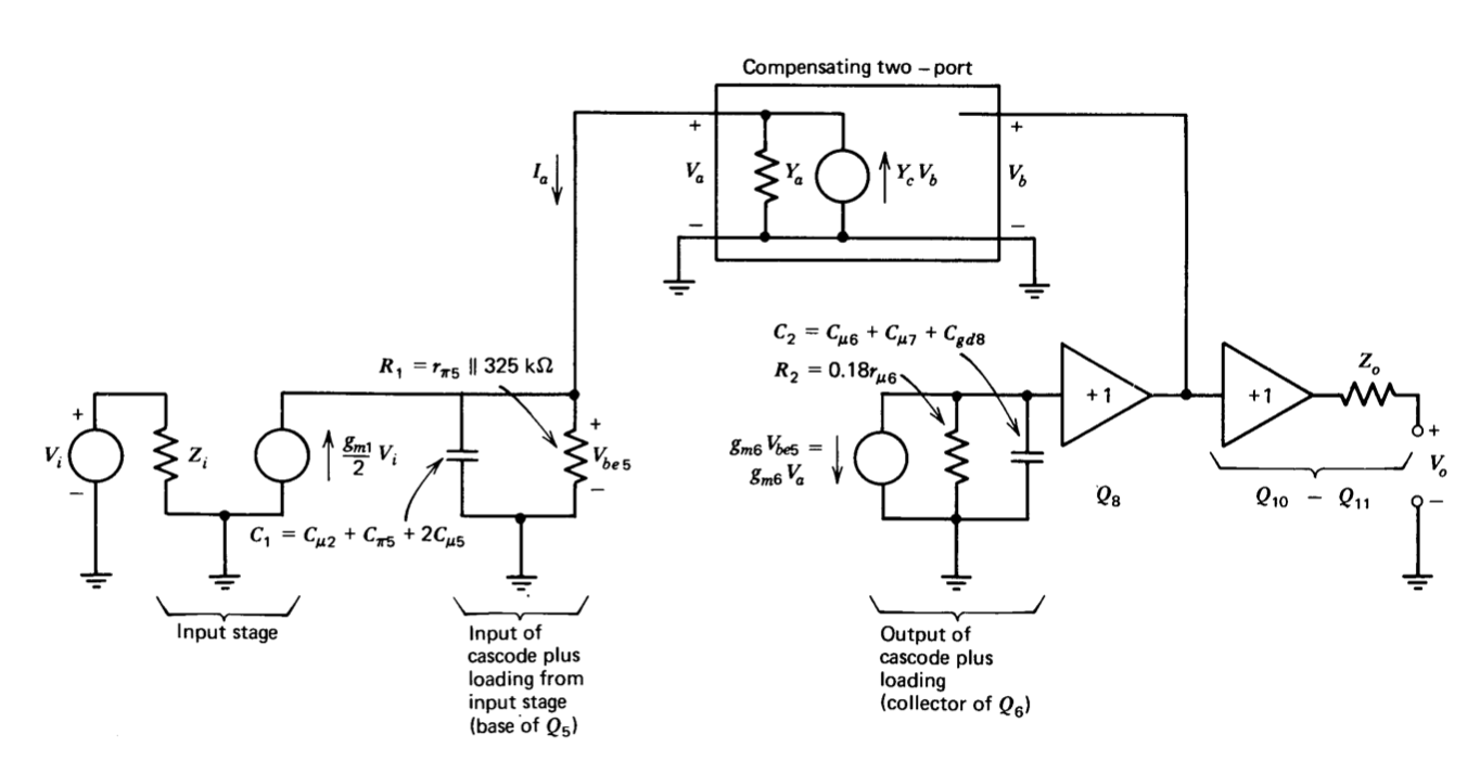
An incremental model for the amplifier of Figure 9.1 that can be used to analyze the effects of the internal feedback used for compensation is shown in Figure 9.6. The development of this model relies heavily on the analysis of Section 9.2.2. The input impedance of the amplifier, which is unimportant for purposes of this calculation, is \(Z_i\). An input voltage forces a proportional current at the node including the base of \(Q_5\).(This representation assumed an input voltage applied to the inverting input of the amplifier. If voltages are applied to both inputs, the differential voltage is used for \(V_i\). An advantage of this type of amplifier is that the dynamics of the first stage do not significantly influence the transfer function at frequencies of interest; thus it functions as a true differential-input amplifier.)
The impedance at the base of \(Q_5\) is modeled as a parallel \(R-C\) network with a time constant equal to \(\tau_b\) in Equation \(\ref{eq9.2.11}\). The remainder of the cascode is modeled as an impedance equal to the impedance from the collector of \(Q_6\) to ground driven by a dependent-current source supplying a current \(g_{m6} V_{be5}\). The impedance transformation of the field-effect transistor is rep resented as a unity-voltage-gain buffer amplifier. The complementary emitter-follower pair is modeled as a second buffer amplifier with an output impedance \(Z_o\).
The compensating minor loop is formed by connecting a two-port network between the output of the source follower and the base of \(Q_5\). Since the right-hand port of the network is driven by the low-impedance source follower, the voltage \(V_b\) is independent of \(V_a\); thus the two-port can be completely represented in this application by the two admittances(These definitions differ from those conventionally used to describe two-port networks in that the reference direction for \(I_a\) is out of the network. This choice reduces the number of minus signs in the following equations.)
\[Y_a = -\dfrac{I_a}{V_a} \ \ \ V_b = 0 \nonumber \]
\[Y_c = -\dfrac{I_a}{V_b} \ \ \ V_a = 0 \nonumber \]
Node equations for the model of Figure 9.6 are
\[\begin{array} {rcl} {\dfrac{g_{m1}}{2} V_i} & = & {(Y_1 + Y_a) V_a - Y_c V_b} \\ {0} & = & {g_{m6} V_a + Y_2 V_b}\label{eq9.2.15} \]
where
\[Y_1 = \dfrac{1}{R_1} + C_1 s \nonumber \]
\[Y_2 = \dfrac{1}{R_2} + C_2 s \nonumber \]
Recognizing that output voltage \(V_o\) is identical to \(V_b\) in the absence of load allows us to determine the gain of the amplifier from Equation \(\ref{eq9.2.15}\) as
\[\dfrac{V_o}{V_i} = \dfrac{V_b}{V_i} = -\dfrac{(g_{m1}/2) g_{m6}/[(Y_1 + Y_a) Y_2]}{1 + g_{m6} Y_c/[(Y_1 + Y_a) Y_2]}\label{eq9.2.16} \]
transmission of the inner loop formed when the amplifier is compensated. In many cases of practical interest, the phase angle of this expression is close to plus or minus \(90^{\circ}\) when its magnitude is unity. The \(90^{\circ}\) phase margin of the compensating loop then insures that there is no peaking in its response. In these cases a very simple approximation serves to determine the magnitude of the open-loop transfer function of the amplifier, and the approximation yields a result that is correct within a factor of 0.707 at all frequencies. The implication from \(\ref{eq9.2.16}\) is that
\[\dfrac{V_o (j\omega)}{V_i (j\omega)} \simeq - \dfrac{g_{m1}}{2Y_c (j\omega )}\label{eq9.2.17} \]
at frequencies where
\[\left |\dfrac{g_{m6} Y_c (j\omega )}{[Y_1 (j\omega ) + Y_a (j\omega )] Y_2 (j\omega )} \right | > 1\nonumber \]
and
\[\dfrac{V_o (j\omega )}{V_i (j\omega )} \simeq -\dfrac{g_{m1}}{2} \dfrac{g_{m6}}{[Y_1 (j\omega ) + Y_a (j\omega )] Y_2 (j\omega )}\label{eq9.2.18} \]
at all other frequencies. Thus, when the minor-loop transmission magnitude is large, the open-loop transfer function of the amplifier is controlled by the minor-loop feedback element.
This approximation is particularly easy to apply graphically. The open-loop transfer function of the amplifier without compensation, but with the compensating network loading the base of \(Q_5\), is plotted on log-magnitude vs. log-frequency coordinates. The proper loading is realized by connecting one side of the network to the base of \(Q_5\) in the usual manner, and by disconnecting the other side of the network from the source of \(Q_8\) and connecting it instead to an incremental ground. This first plot is particularly easy to obtain if a single capacitor is used as the compensating element (the most frequent case because this compensation leads to an approximately single pole open-loop transfer function) since only the location of the higher-frequency pole in Equation \(\ref{eq9.2.12}\) is changed. The magnitude of the expression \(g_{m1}/2 Y_e(j\omega )\) is also plotted on the same coordinates. The magnitude of the amplifier open-loop transfer function at any frequency is then approximately equal to the lower magnitude of the two plotted curves. This relationship is easily developed from Equations \(\ref{eq9.2.17}\) and \(\ref{eq9.2.18}\), by noticing that the gain of the amplifier with the shorted compensating network connected to the base of \(Q_5\) is
\[\dfrac{g_{m1}}{2} \dfrac{g_{m6}}{(Y_1 + Y_a) Y_2}\nonumber \]
and that if
\[\left | \dfrac{g_{m1}}{2Y_c} \right | < \left | \dfrac{g_{m1}}{2} \dfrac{g_{m6}}{(Y_1 + Y_a) Y_2} \right |\nonumber \]
then
\[\left | \dfrac{g_{m6} Y_c}{(Y_1 + Y_a) Y_2} \right | > 1\nonumber \]
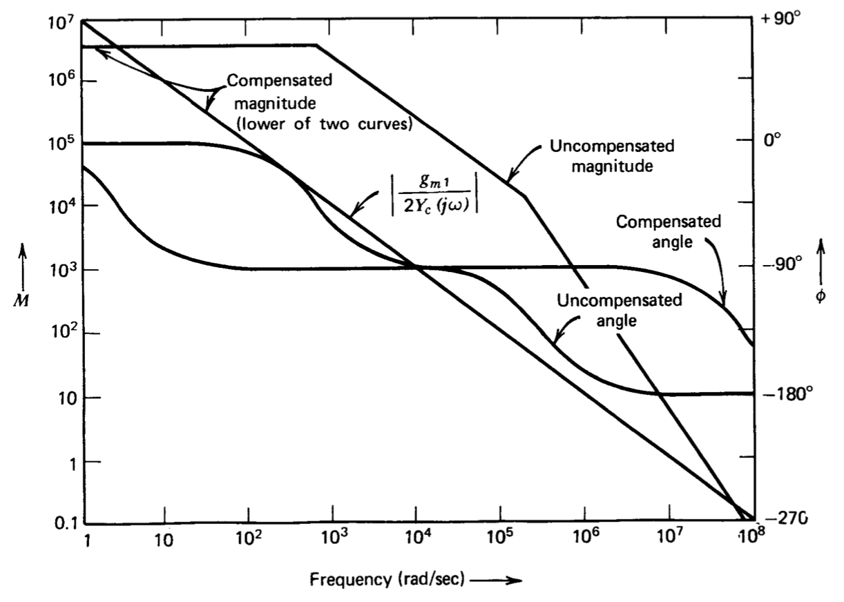
Figure 9.7 illustrates the effects of compensating the amplifier shown in Figure 9.1 with a 20-pF capacitor. The quantities \(Y_c\) and \(Y_a\) for this compen sating network are both equal to \(2 \times 10^{-11}s\). One of the two curves is obtained directly from the uncompensated transfer function of Figure 9.5 by moving the second pole from \(2.2 \times 10^5\) radians per second to \(1.5 \times 10^5\) radians per second, since loading by the compensating capacitor increases the total capacitance at the base of \(Q_5\) by 50%. The second plot is
\[\left | \right | = \dfrac{10^7}{\omega } \nonumber \]
The curve for the compensated amplifier is the lower of the two plots at all frequencies.
The advantages of this compensation for certain applications are obvious. It was shown earlier that operation with \(f = 1\) would cause the un compensated amplifier to oscillate. If a 20-pF compensating capacitor is used, the phase margin of the amplifier with direct feedback is greater than \(45^{\circ}\).
Note that this compensation lowers the first amplifier open-loop pole to 2.5 radians per second. The location of the low-frequency pole cannot be independently chosen if we insist on a single-pole rolloff at frequencies
below the unity-gain frequency and constrain both the unity-gain frequency and the d-c gain. The pole must be located at a frequency equal to the ratio of the unity-gain frequency to the d-c gain. This pole does not compromise closed-loop bandwidth, since closed-loop bandwidth is determined by the crossover frequency of the loop.
It is worth mentioning that parameter values for this amplifier are such that the uncompensated open-loop transfer function will be noticeably modified by any capacitive compensation in excess of approximately 0.1 pF! The minimum capacitor value necessary to modify the amplifier transfer function can be determined by noting that the uncompensated magnitude curve shown in Figure 9.5 includes a region where its value is \(2 \times 10^9/\omega \) Thus, if a capacitor in excess of 0.1 pF is used for compensation, the magnitude \([g_{m1}/2 Y_c(j\omega )\) will be smaller than the uncompensated magnitude over some frequency range. Furthermore, it is evident that feedback from any high level part of the circuit (from the collector of \(Q_6\) on) back to the base circuit of Q5 has approximately the same effect as feedback via the compensation terminals. Inevitable stray capacitance between these two parts of the circuit is usually on the order of 1 pF, and it is therefore concluded that the "uncompensated" curve of Figure 9.7 can probably never be measured for an actual amplifier.
As indicated above, feedback from any portion of the circuit from the collector of \(Q_6\) on modifies performance in much the same way as feed back from the source of \(Q_8\), and in certain applications it may be advantageous to compensate by feeding back from an alternate point. For ex ample, feedback from the output terminal includes more of the amplifier inside the compensating loop and thus with the control of this loop. Unfortunately, compensating-loop stability is less certain for this type of minor-loop feedback. Similarly, if large capacitors are used for compensation, greater inner-loop stability may be achieved by compensating from the collector \(Q_6\).
Some of the reasons for selecting an amplifier topology with the possibility for this type of compensation should now be clear. The compensation is normally chosen so that it, rather than uncompensated amplifier dynamics, dominates amplifier performance at all frequencies of interest. Thus the open-loop transfer function of the amplifier with compensation becomes quite reliable. A wide variety of open-loop transfer functions can be obtained (several examples will be given in Chapter 13) with the main limitation being the requirement of maintaining the stability of the compensating loop. Furthermore, it is easy to determine what compensating network should be used to produce a given open-loop transfer function.