
10.4: REPRESENTATIVE INTEGRATED-CIRCUIT OPERATIONAL AMPLIFIERS
- Page ID
- 74434

A number of semiconductor manufacturers presently offer a variety of integrated-circuit operational amplifiers. While an exhaustive study of available amplifiers is beyond the scope of this book, an examination of several representative designs demonstrates some of the possible variations of the basic topology described in Chapters 8 and 9 and serves as a useful prelude to the material on applications.
It should be mentioned that most of the circuits described are popular enough to be built, often with minor modifications, by a number of manufacturers. These "second-source" designs usually retain a designation that maintains an association with the original. Another factor that contributes to the proliferation of part numbers is that most manufacturers divide their production runs into two or three categories on the basis of measured parameters such as input bias current and offset voltage as well as the temperature range over which specifications are guaranteed. For example, National Semiconductor uses the 100, 200, and 300 series to designate whether military, intermediate, or commercial temperature range specifications are met, while Fairchild presently suffixes a C to designate commercial temperature range devices.
We should observe that no guarantee of inferior performance is implied when the less splendidly specified devices are used. Since all devices in one family are made by an identical process and since yields are constantly improving, a logical conclusion is that many commercially specified devices must in fact be meeting military specifications. These considerations coupled with a dramatic cost advantage (the order of a factor of three) suggest the use of the commercial devices in all but the most exacting applications.
and LM101A Operational Amplifiers
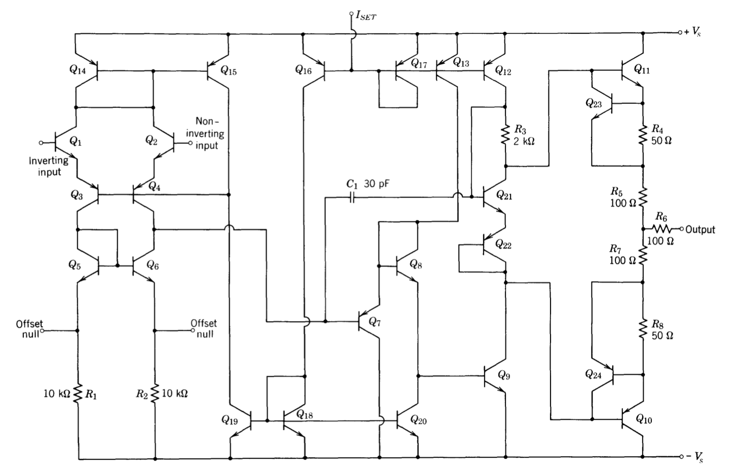
The LM101 operational amplifier(R. J. Widlar, "A New Monolithic Operational Amplifier Design," National Semicon ductor Corporation, Technical Paper TP-2, June, 1967. ) occupies an important place in the history of integrated-circuit amplifiers since it was the first design to use the two-stage topology combined with minor-loop feedback for compensation. Its superiority was such that it stimulated a variety of competing designs as well as serving as the ancestor of several more advanced National Semiconductor amplifiers. of this amplifier are both proportional to the reciprocal of the base-width modulation factor and thus are comparable in magnitude.
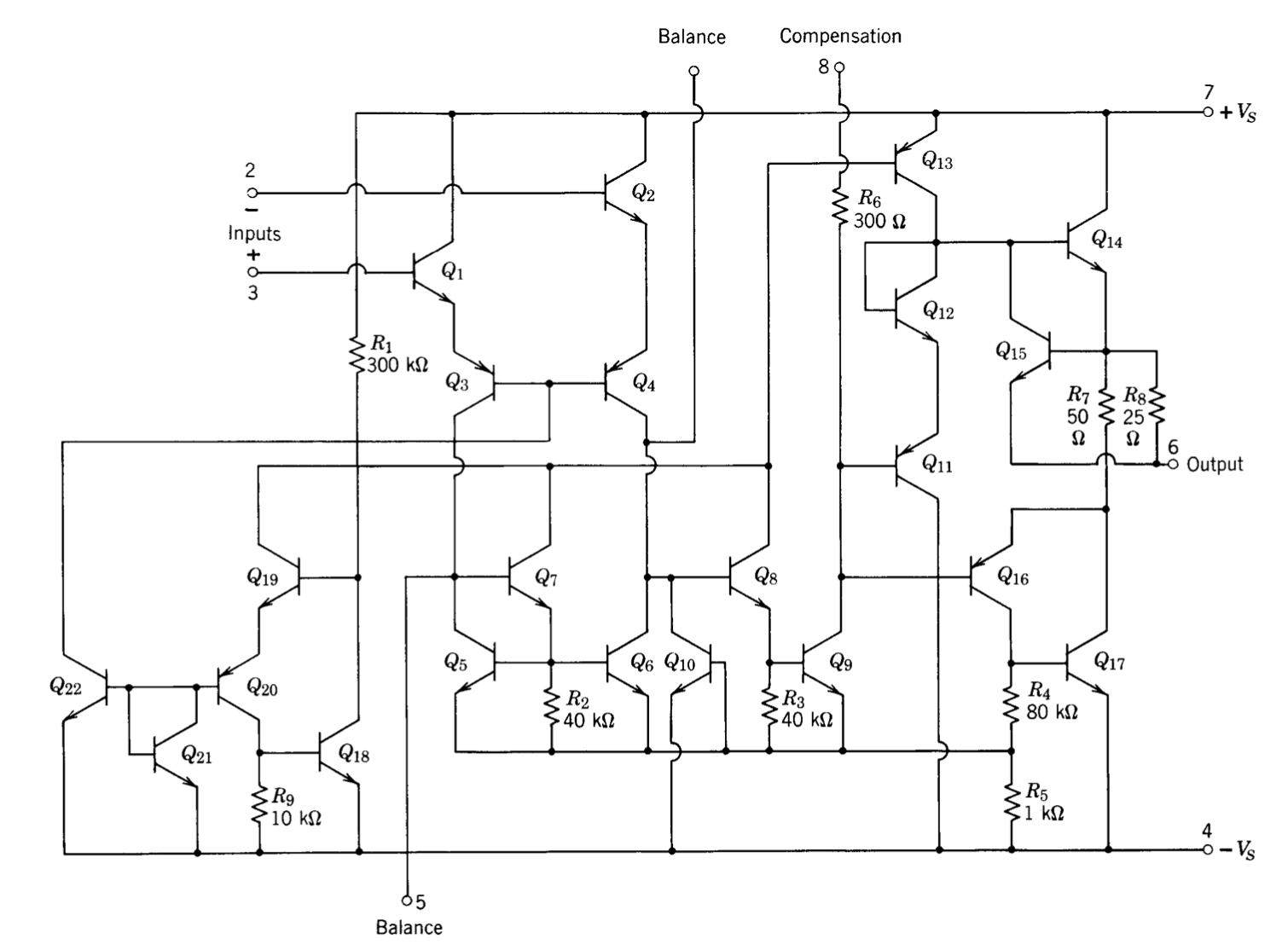
The schematic diagram for the amplifier is shown in Figure 10.17, and specifications are included in Table 10.1. (The definitions of some of the specified quantities are given in Chapter 11.) As was the case with the discrete-component amplifier described in the last chapter, it is first necessary to identify the functions of the various transistors, with emphasis placed on the transistors in the gain path. Transistors \(Q_1\) through \(Q_4\) form a differential input connection as described in the last section. The \(Q_5\) through \(Q_7\) triad is a current-repeater load for the differential stage. Transistors \(Q_8\) and \(Q_9\) are connected as an emitter follower driving a high voltage gain common-emitter stage. The voltage gains of the first and second stages
Table 10.1 LM101 Specifications: Electrical Characteristics
| Parameter | Condition | Min | Typ | Max | Units |
| Input offset voltage | \(T_A = 25^{\circ} C, R_S \le 10 k \Omega\) | 1.0 | 5.0 | mV | |
| Input offset current | \(T_A = 25^{\circ} C\) | 40 | 200 | nA | |
| Input bias current | \(T_A = 25^{\circ} C\) | 120 | 500 | nA | |
| Input resistance | \(T_A = 25^{\circ} C | 300 | 800 | \(k\Omega\) | |
| Supply current | \(T_A = 25^{\circ} C, V_S = \pm 20\ V\) | 1.8 | 3.0 | mA | |
| Large-signal voltage gain | \(T_A = 25^{\circ} C, V_S = \pm 15\ V\) \(V_{\text{out}} = \pm 10V, R_L \ge 2\ k\Omega\) |
50 | 160 | V/mV | |
| Input offset voltage | \(R_S \le 10\ k\Omega\) | 6.0 | mV | ||
| Average temperature | \(R_S \le 50\ \Omega\) | 3.0 | \(\mu V/^{\circ} C\) | ||
| coefficient of input | |||||
| offset voltage | \(R_S \le 10\ k\Omega\) | 6.0 | \(\mu V/^{\circ} C\) | ||
| Input offset current | \(T_A = +125^{\circ} C\) | 10 | 200 | nA | |
| \(T_A = - 55^{\circ} C\) | 100 | 500 | nA | ||
| Input bias current | \(T_A = - 55^{\circ} C\) | 0.28 | 1.5 | \(\mu A\) | |
| Supply current | \(T_A = +125^{\circ} C, V_S = \pm 20\ V\) | 1.2 | 2.5 | mA | |
| Large-signal voltage gain | \(V_S = \pm 15\ V, V_{\text{out}} = \pm 10\ V\) \(R_L \ge 2\ k\Omega\) |
25 | V/mV | ||
| Output voltage swing | \(V_S = \pm 15\ V, R_L = 10\ k\Omega\) | \(\pm 12\) | \(\pm 14\) | V | |
| \(R_L = 2\ k \Omega\) | \(\pm 10\) | \(\pm 13\) | V | ||
| Input voltage range | \(V_S = \pm 15\ V\) | \(\pm 12\) | V | ||
| Common-mode rejection ratio | \(R_S \le 10 \ k\Omega\) | 70 | 90 | dB | |
| Supply-voltage rejection ratio | \(R_S \le 10 \ k\Omega\) | 70 | 90 | dB |
The complementary Darlington connection \(Q_{16}\) and \(Q_{17}\) supplies negative output current. The use of this connection augments the low gain of the lateral PNP. (Recall that this amplifier was manufactured when current gains of 5 to 10 were anticipated from lateral-PNP transistors.) While a vertical-PNP transistor could have been used in the output stage, the designer of the 101 elected the complementary Darlington since it reduced total chip area(t is interesting to note that the size of the LMI0I chip is 0.045 inch square, smaller than many single transistors.) and since processing was simplified.
Positive output current is supplied by \(Q_{14}\). The gain path from the collector of \(Q_9\) to the emitter of \(Q_{14}\) includes transistor \(Q_{11}\), another lateral PNP. This device matches the current gain from the collector of \(Q_9\) to the output for positive output swings with the gain for negative output swings. By locating current source \(Q_{13}\) in the emitter circuit of \(Q_{11}\), this current source provides bias for \(Q_{11}\) as well as a high-resistance load for \(Q_9\). Diode-connected transistor \(Q_{12}\) is included in the output circuit to reduce cross over distortion.
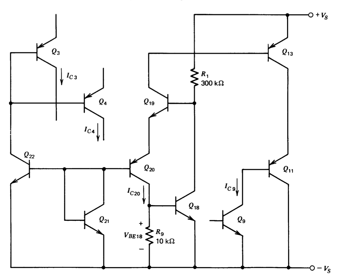
The operation of the biasing circuit for the LM101 depends on achieving equal current gains from certain lateral-PNP transistors. This approach was used since while low, unpredictable gains characterized the lateral PNP's of the era, the performance was highly uniform from device to device on one chip. The transistors used for biasing are shown in Figure 10.18. The loop containing transistors \(Q_{18}\), \(Q_{19}\), and \(Q_{20}\) controls \(I_{C20}\) so that \(I_{C20} \simeq V_{BE18}/R_9 \simeq 60\ \mu A\).
The high-value resistor, \(R_1\), included in this circuit is a collector FET. The characteristics of this resistor make the current supplied by it relatively independent of supply voltage. The base current of \(Q_{20}\) is repeated by tran sistors \(Q_{21}\) and \(Q_{22}\) and applied to the common-base connection of \(Q_3\) and \(Q_4\). If the areas of \(Q_{21}\) and \(Q_{22}\) and the current gains of \(Q_3\), \(Q_4\), and \(Q_{20}\) were equal, the total first-stage collector current, \(I_{C3} + I_{C4}\), would be equal to \(I_{C20}\). The area of \(Q_{21}\) is actually made larger than that of \(Q_{22}\) so that each input transistor operates at a quiescent collector current of \(10\ \mu A\).
Biasing for transistor \(Q_9\) includes transistors \(Q_{11}\), \(Q_{13}\), \(Q_{19}\), and \(Q_{20}\). Assuming high gain from \(Q_{19}\),
\[I_{C9} = \dfrac{I_{C20} (\beta_{20} + 1)}{\beta_{20}} \dfrac{\beta_{13}}{(1 + \beta_{11})} \nonumber \]
Thus \(I_{C9} = I_{C20}\) for equal PNP gains.
The actual circuit (Figure 10.17) shows that the collectors of \(Q_7\) and \(Q_8\) are connected in parallel with that of \(Q_{19}\). This doesn't significantly alter opera tion since \(I_{C19} \gg I_{C7} \simeq I_{C8}\), and allows a smaller geometry chip since \(Q_7\), \(Q_8\), and \(Q_{19}\) can all be located in the same isolation diffusion.
Positive output current is limited by transistor \(Q_{15}\) (Figure 10.17) when the voltage across \(R_8\) becomes approximately 0.6 volt. The negative current limit
is more involved. When the voltage across \(R_7\) reaches approximately 1.2 volts, the collector-to-base junction of \(Q_{15}\) becomes forward biased, and further increases in output current are supplied by Qu,. Since this lateral PNP has low gain, the emitter current of \(Q_9\) increases significantly when the limiting value of output current is reached. The emitter current of \(Q_9\) flows through \(R_5\), and when the drop across this resistor reaches 0.6 volt, transistor \(Q_{10}\) limits base drive for \(Q_8\), preventing further increases in output current.
There are two reasons for this unusual limiting circuit. First, the peculiarities of lateral PNP \(Q_{16}\) make it advantageous to have relatively high resistance between the emitter of this transistor and the output of the circuit to insure stability with capacitive loads. Second, this limit also protects \(Q_9\) if its collector is clamped to some voltage level. Such clamping applied to point 8 can be used to limit the output voltage of the amplifier.
The amplifier can be balanced to reduce input offset voltage by connecting a high-value resistor (typically \(20\ M\Omega\) to \(100\ M\Omega\)) from either point 5 or point 1 to ground. This type of balancing results in minimum voltage drift from the input transistors.
Compensating minor-loop feedback around the high-gain portion of the circuit is applied between points 1 to 8. The \(300-\Omega\) resistor in this circuit provides a zero at a frequency approximately one decade above the amplifier unity-gain frequency when a capacitor is used for compensation. The positive phase shift associated with this zero improves amplifier stability.
Measurements made on the amplifier show that the transconductance from the input terminals to the base of \(Q_8\) is approximately \(2 \times 10^{-4}\) mho so that the open-loop transfer function of the amplifier at frequencies of interest is approximately \(2 \times 10^{-4}/Y_c\), where \(Y_c\) is the short-circuit transfer admittance of the compensating network as defined in Section 9.2.3. This value of transconductance is consistent with the four series-connected input transistors operating at \(10\ \mu A\) of quiescent current. The transconductance to either output of the differential pair is \(qI_C/4kT \simeq 10^{-4}\text{ mho}\), and this value is doubled by the current-repeater load used for the input stage. While the compensating network does load the high-impedance node at the collector of \(Q_9\), such loading is usually insignificant.
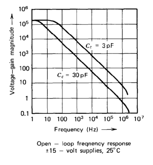
The open-loop transfer function included as part of the specifications shows that the amplifier has a single-pole response with a unity-gain frequency of approximately 1 MHz when compensated with a \(30-pF\) capacitor. This result can also be obtained from the analytic expression given above. The amplifier dynamics other than those which result from the inner loop limit the crossover frequency of loops using this amplifier to between 1 and 2 MHz. The phase shift that leads to instability for higher crossover frequencies results primarily from the lateral PNP transistors in the input stage.
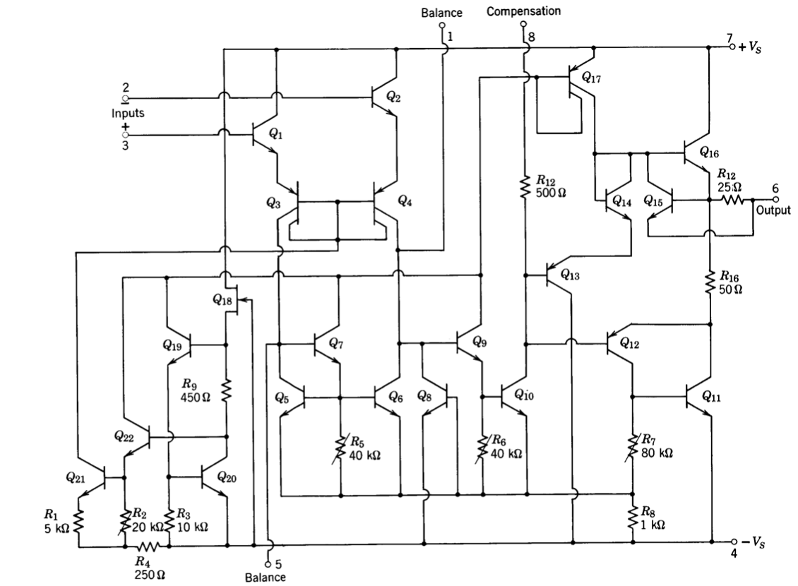
Evolutibnary modifications changed the LM101 amplifier to the LM101A shown in Figure 10.19, and this amplifier is (as of this writing) still the standard to which all other general-purpose, externally compensated integrated operational amplifiers are compared. The differences reflect primarily the increased performance of components available at the time the LM101A was designed. Better matching tolerances reduced the maximum input offset voltage to \(2\ mV\) at \(25^{\circ} C\) and improved common-mode rejection ratio and power-supply rejection modestly. Improved input-transistor current gain and a modified bias circuit reduced the maximum input bias current over the full \(-55^{\circ} C\) to \(+ 125^{\circ} C\) temperature range to \(100\ nA\) and reduced the typical room-temperature offset current to \(1.5\ nA\).
A detailed discussion of the bias circuit of the LM101A (transistors \(Q_{18}\) through \(Q_{22}\) in Figure 10.19) is beyond the scope of the book.(R. J. Widlar, "I. C. Op Amp with Improved Input-Current Characteristics," EEE, pp. 38-41, December, 1968. ) Its most important functional characteristic is that the quiescent collector current of the input stage is made proportional to absolute temperature. As a result, the transconductance of the input stage (which has a direct effect on the compensated open-loop transfer function of the amplifier) is made virtually temperature independent. A subsidiary benefit is that the change in quies cent current with temperature partially offsets the current-gain change of the input transistors so that the temperature dependence of the input bias current is reduced. The modified bias circuit became practical because the improved gain stability of the controlled-gain lateral PNP's used in the LM101A eliminated the requirement for the bias circuit to compensate for gross variations in lateral-PNP gain.
We shall get a greater appreciation for the versatility of the LM101A, particularly with respect to the control of its dynamics afforded by various types of compensation, in Chapter 13.
Table 10.2 \(\mu A 776\) specifications: \(\pm 15\) Volt Operation for 776; Electrical Characteristics (\(T_A\) is \(25^{\circ} C\), unless otherwise specified)
| \(I_{SET} = 1.5\ \mu A\) | \(I_{SET} = 15\ \mu A\) | |||||||
| Parameter | Conditions | Min | Type | Max | Min | Typ | Max | Units |
| Input offset voltage | \(R_S \le 10\ k\Omega\) | 2.0 | 5.0 | 2.0 | 5.0 | \(mV\) | ||
| Input offset current | 0.7 | 3.0 | 2.0 | 15 | \(nA\) | |||
| Input bias current | 2.0 | 7.5 | 15 | 50 | \(nA\) | |||
| Input resistance | 50 | 5.0 | \(M\Omega\) | |||||
| Input capacitance | 2.0 | 2.0 | \(pF\) | |||||
| Offset voltage adjustment range | 9.0 | 18 | \(mV\) | |||||
| Large-signal voltage gain | \(R_L \ge 75\ k\Omega, V_{\text{out}} = \pm 10\ V\) | 200 | 400 | \(V/mV\) | ||||
| \(R_L \ge 5\ k\Omega, V_{\text{out}} = \pm 10\ V\) | 100 | 400 | \(V/mV\) | |||||
| Output resistance | 5.0 | 1.0 | \(k\Omega\) | |||||
| Output short-circuit current | 3.0 | 12 | \(mA\) | |||||
| Supply current | 20 | 25 | 160 | 180 | \(\mu A\) | |||
| Power consumption | 0.75 | 5.4 | \(mW\) | |||||
| Transient response Rise time (unity gain) |
\(V_{in} = 20\ mV, R_L \ge 5\ k\Omega\), \(C_L = 100\ pF\) |
1.6 | 0.35 | \(\mu S\) | ||||
| Overshoot | 0 | 10 | % | |||||
| Slew rate | \(R_L \ge 5\ k\Omega\) | 0.1 | 0.8 | \(V/\mu S\) | ||||
| Output voltage swing | \(R_L \ge 75 \ k\Omega\) | \(\pm 12\) | \(\pm 14\) | \(V\) | ||||
| \(R_L \ge 5 \ k\Omega\) | \(\pm 10\) | \(\pm 13\) | \(V\) | |||||
| The following specifications apply: \(-55^{\circ} C \le T_A \le + 125^{\circ} C\) | ||||||||
| Input offset voltage | \(R_S \le 10 \ k\Omega\) | 6.0 | 6.0 | \(mV\) | ||||
| Input offset current | \(T_A = + 125^{\circ} C\) | 5.0 | 15 | \(nA\) | ||||
| \(T_A = -55^{\circ} C\) | 10 | 40 | \(nA\) | |||||
| Input bias current | \(T_A = + 125^{\circ} C\) | 7.5 | 50 | \(nA\) | ||||
| \(T_A = - 55^{\circ} C\) | 20 | 120 | \(nA\) | |||||
| Input-voltage range | \(\pm 10\) | \(\pm 10\) | \(V\) | |||||
| Common-mode rejection ratio | \(R_S \le 10\ k\Omega\) | 70 | 90 | 70 | 90 | \(dB\) | ||
| Supply-voltage rejection ratio | \(R_S \le 10\ k\Omega\) | 25 | 150 | 25 | 150 | \(\mu V/V\) | ||
| Large-signal voltage swing | \(R_L \ge 75 \ge 75 \ k\Omega\), \(V_{\text{out}} = \pm 10\ V\) | 100 | 75 | \(V/mV\) | ||||
| Output voltage swing | \(R_L \ge 75 \ge 75 \ k\Omega\) | \(\pm 10\) | \(\pm 10\) | \(V\) | ||||
| Supply current | 30 | 200 | \( mA\) | |||||
| Power consumption | 0.9 | 6.0 | \(mW\) | |||||
\(\mu A776\) Operational Amplifier
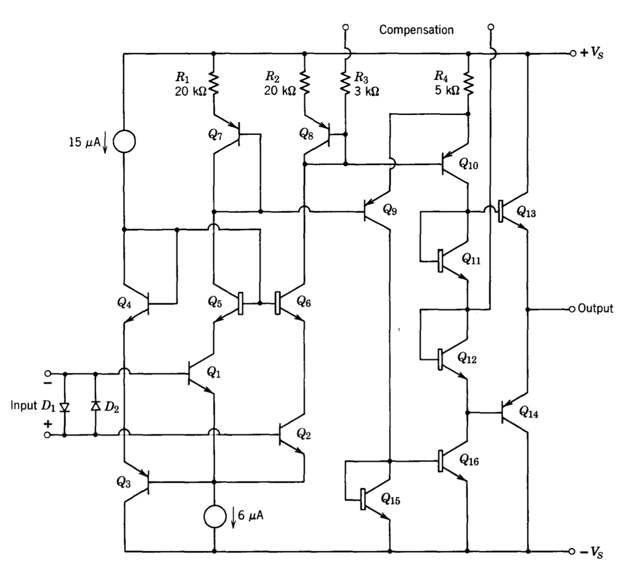
The LM101A circuit described in the previous section can be tailored for use in a variety of applications by choice of compensation. An interesting alternative way of modifying amplifier performance by changing its quiescent operating currents is used in the \(\mu A776\) operational amplifier. Some of the tradeoffs that result from quiescent current changes were discussed in Section 9.3.3, and we recall that lower operating currents compromise bandwidth in exchange for reduced input bias current and power consumption.
The schematic diagram for this amplifier is shown in Figure 10.20, with performance specifications listed in Table 10.2. Several topological similarities between this amplifier and the LM101 are evident. Transistors \(Q_1\) through \(Q_6\) form a current-repeater-loaded differential input stage. Transistors \(Q_7\) and Q9 are an emitter-follower common-emitter combination loaded by current source \(Q_{12}\). Diode-connected transistors \(Q_{21}\) and \(Q_{22}\) forward bias the \(Q_{10}-Q_{11}\) complementary output pair. Capacitor \(C_1\) compensates the amplifier.
The unique feature of the \(\mu A776\) is that all quiescent operating currents are referenced to the current labeled \(I_{SET}\) in the schematic diagram by means of a series of current repeaters. Thus changing this set current causes proportional changes in all quiescent currents and scales the current- dependent amplifier parameters.
The collector current of \(Q_{19}\) is proportional to the set current because of the \(Q_{16}-Q_{18}-Q_{19}\) connection. The difference between this current and the collector current of \(Q_{15}\) is applied to the common-base connection of the \(Q_3-Q_4\) pair. The collector current of \(Q_{15}\) is proportional to the total quies cent operating current of the differential input stage, since \(Q_{14}\) and \(Q_{15}\) form a current repeater for the sum of the collector currents of \(Q_1\) and \(Q_2\). The resultant negative feedback loop stabilizes quiescent differential-stage current. The geometries of the various transistors are such that the quies cent collector currents of \(Q_1, Q_2, Q_3\), and \(Q_4\) are each approximately equal to \(I_{SET}\).
The amplifier can be balanced by changing the relative values of the emitter resistors of the \(Q_5-Q_6\) current-repeater pair via an external potentiometer. While this balance method does not equalize the base-to-emitter voltages of the \(Q_5-Q_6\) pair, any drift increase is minimal because of the excellent match of first-stage components. An advantage is that the external balance terminals connect to low-impedance circuit points making the amplifier less susceptible to externally-generated noise.
One of the design objectives for the \(\mu A776\) was to make input- and output-voltage dynamic ranges close to the supply voltages so that low-voltage operation became practical. For this purpose, the vertical PNP \(Q_7\) is used as the emitter-follower portion of the high-gain stage. The quiescent voltage at the base of \(Q_7\) is approximately the same as the voltage at the base of \(Q_9\) (one diode potential above the negative supply voltage) since the base-to-emitter voltage of \(Q_7\) and the forward voltage of diode-connected transistor Qs are comparable. (Current sources \(Q_{13}\) and \(Q_{20}\) bias \(Q_7\) and \(Q_8\).) Because the operating potential of \(Q_7\) is close to the negative supply, the input stage remains linear for common-mode voltages within about 1.5 volts of the negative supply.
Transistor \(Q_{21}\) is a modified diode-connected transistor which, in conjunction with \(Q_{22}\), reduces output stage crossover distortion. At low set-current levels (resulting in correspondingly low collector currents for \(Q_9\) and \(Q_{12}\)) the drop across \(R_3\) is negligible, and the potential applied between the bases of \(Q_{10}\) and \(Q_{11}\) is equal to the sum of the base-to-emitter voltages of \(Q_{21}\) and \(Q_{22}\). At higher set currents, the voltage drop across \(R_3\) lowers the ratio of output-stage quiescent current to that of \(Q_9\) as an aid toward maintaining low power consumption.
A vertical-PNP transistor is used in the complementary output stage, and this stage, combined with its driver (\(Q_9\) and \(Q_{12}\)), permits an output voltage dynamic range within approximately one volt of the supplies at low output currents. Current limiting is identical to that used in the discrete-component amplifier described in Chapter 9.
The ability to change operating currents lends itself to rather interesting applications. For example, operation with input bias currents in the picoampere region and power consumption at the nanowatt level is possible with appropriately low set current if low bandwidth is tolerable. The amplifier can also effectively be turned into an open circuit at its input and output terminals by making the set current zero, and thus can be used as an analog switch. Since the unity-gain frequency for this amplifier is \(g_m/(2 \times 30\ pF)\) where \(g_m\), is the (assumed equal) transconductance of transistors \(Q_1\) through \(Q_4\), changes in operating current result in directly proportional changes in unity-gain frequency.
This amplifier is inherently a low-power device, even at modest set-current levels. For example, many performance specifications for a \(\mu A776\) operating at a set current of \(10\ \mu A\) are comparable to those of an LM101A when compensated with a \(30-pF\) capacitor. However, the power consumption of the \(\mu A776\) is approximately \(3\ mW\) at this set current (assuming operation from 15-volt supplies) while that of the LM101A is \(50\ mW\). The difference reflects the fact that the operating currents of the second and output stage are comparable to that of the first stage in the \(\mu A776\), while higher relative currents are used in the LM101A. One reason that this difference is possible is that the slew rate of the \(\mu A776\) is limited by its fixed, \(30-pF\) compensating capacitor. Higher second-stage current is necessary in the LM101A to allow higher slew rates when alternate compensating networks are used.
Table 10.3 LM108 Specifications: Electrical Characteristics
| Parameter | Conditions | Min | Type | Max | Units |
| Input offset voltage | \(T_A = 25^{\circ} C\) | 0.7 | 2.0 | \(mV\) | |
| Input offset current | \(T_A = 25^{\circ} C\) | 0.05 | 0.2 | \(nA\) | |
| Input bias current | \(T_A = 25^{\circ} C\) | 0.8 | 2.0 | \(nA\) | |
| Input resistance | \(T_A = 25^{\circ} C\) | 30 | 70 | \(M\Omega\) | |
| Supply current | \(T_A = 25^{\circ} C\) | 0.3 | 0.6 | \(mA\) | |
| Large-signal voltage gain | \(T_A = 25^{\circ} C, V_S = \pm 15\ V\) \(V_{\text{out}} = \pm 10\ V, R_L \ge 10\ k\Omega\) |
50 | 300 | \(V/mV\) | |
| Input offset voltage | 3.0 | \(mV\) | |||
| Average temperature coefficient of input-offset voltage |
3.0 | 15 | \(\mu V /^{\circ} C\) | ||
| Input offset current | 0.4 | \(nA\) | |||
| Average temperature coefficient of input offset current |
0.5 | 2.5 | \(pA/^{\circ} C\) | ||
| Input bias current | 3.0 | \(nA\) | |||
| Supply current | \(T_A = +125^{\circ} C\) | 0.15 | 0.4 | \(mA\) | |
| Large-signal voltage gain | \(V_S = \PM 15\ V, V_{\text{out}} = \pm 10\ V\) \(R_L \ge 10\ k\Omega\) |
25 | \(V/mV\) | ||
| Output voltage swing | \(V_S = \pm 15\ V, R_L = 10\ k\Omega\) | \(\pm 13\) | \(\pm 14\) | \(V\) | |
| Input voltage range | \(V_S = \pm 15\ V\) | \(\pm 14\) | \(V\) | ||
| Common-mode rejection ratio | 85 | 100 | \(dB\) | ||
| Supply-voltage rejection ratio | 80 | 96 | \(dB\) |
Operational Amplifier
R. J. Widlar, "I. C. Op Amp Beats FET's on Input Current," National Semiconductor Corporation, Application note AN-29, December, 1969.
The LM108 operational amplifier was the first general-purpose design to use super \(\beta\) transistors in order to achieve ultra-low input currents. While a detailed discussion of the operation of this circuit is beyond the scope of this book, the LM108 does illustrate another of the many useful ways that the basic two-stage topology can be realized.
A simplified schematic diagram that illustrates some of the more important features of the design is shown in Figure 10.21, with specifications given in Table 10.3. (The complete circuit, which is considerably more complex, is described in the reference given in the footnote.) The schematic diagram indicates two types of NPN transistors. Those with a narrow base (\(Q_1\), \(Q_2\), and \(Q_4\)) are super \(\beta\) transistors with current gains of several thousand and low breakdown voltage. The wide-base NPN transistors are conventional devices.
The input differential pair operates at a quiescent current level of \(3 \mu A\) per device. This quiescent level combined with the high gain of \(Q_1\) and \(Q_2\) results in an input bias current of less than one nanoampere, and thus the LM108 is ideally suited to use in high-impedance circuits.
In order to prevent voltage breakdown of the input transistors, their collectors are bootstrapped via cascode transistors \(Q_5\) and \(Q_6\). Operating currents and geometries of transistors \(Q_3, Q_4, Q_5\), and \(Q_6\) are chosen so that the input transistors operate at nearly zero collector-to-base voltage. Thus collector-to-base leakage current (which can dominate input current at elevated temperatures) is largely eliminated. It is also necessary to diode clamp the input terminals to prevent breaking down input transistors under large-signal conditions. This clamping, which deteriorates performance in some nonlinear applications, is one of the prices paid for low input current.
Transistors \(Q_9\) and \(Q_{10}\) form a second-stage differential amplifier. Diode-connected transistors Q7 and \(Q_8\) compensate for the base-to-emitter voltages of \(Q_9-Q_{10}\), so that the quiescent voltage across \(R_4\) is equal to that across \(R_1\) or \(R_2\). Resistor values are such that second-stage quiescent current is twice that of the first stage. Transistors \(Q_{15}\) and \(Q_{16}\) connected as a current repeater reflect the collector current of \(Q_9\) as a load for \(Q_{10}\). This connection doubles the voltage gain of the second stage compared with using a fixed-magnitude current source as the load for \(Q_{10}\). The high-resistance node is buffered with a conventional output stage.
Compensation can be effected by forming an inner loop via collector-to-base feedback around \(Q_{10}\). Circuit parameters are such that single-pole compensation with dynamics comparable to the feedback-compensated case results when a dominant pole is created by shunting a capacitor from the high-resistance node to ground. This alternate compensation results in superior supply-voltage noise rejection. (One disadvantage of capacitive coupling from collector to base of a second-stage transistor is that this feedback forces the transistor to couple high-frequency supply-voltage transients applied to its emitter directly to the amplifier output.)
The dynamics of the LM108 are not as good as those of the LM101A. While comparable bandwidths are possible in low-gain, resistively loaded applications, the bandwidth of the LM101A is substantially better when high closed-loop voltage gain or capacitive loading is required. The slower dynamics of the LM108 result in part from the use of the lateral PNP'S in the second stage where their peculiarities more directly affect bandwidth and partially from the low quiescent currents used to reduce the power consumption of the circuit by a factor of five compared with that of the LM1OIA.
LMI10 Voltage Follower
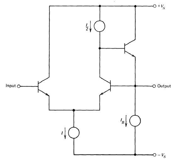
The three amplifiers described earlier in this section have been general-purpose operational amplifiers where one design objective was to insure that the circuit could be used in a wide variety of applications. If this requirement is relaxed, the resultant topological freedom can at times be
exploited. Consider the simplified amplifier shown in Figure 10.22. Here a current-source-loaded differential amplifier is used as a single high-gain stage and is buffered by an emitter follower. The emitter follower is biased with a current source. This very simple operational amplifier is connected in a unity-gain noninverting or voltage-follower configuration. Since it is known that the input and output voltage levels are equal under normal operating conditions, there is no need to allow for arbitrary input-output voltage relationships. One very significant advantage is that only NPN transistors are included in the gain path, and the bandwidth limitations that result from lateral PNP transistors are eliminated.
This topology is actually a one-stage amplifier, and the dynamics associated with such designs are even more impressive than those of two-stage amplifiers. While the low-frequency open-loop voltage gain of this design may be less than that of two-stage amplifiers, open-loop voltage gains of several thousand result in adequate desensitivity when direct output-to-input feedback is used.
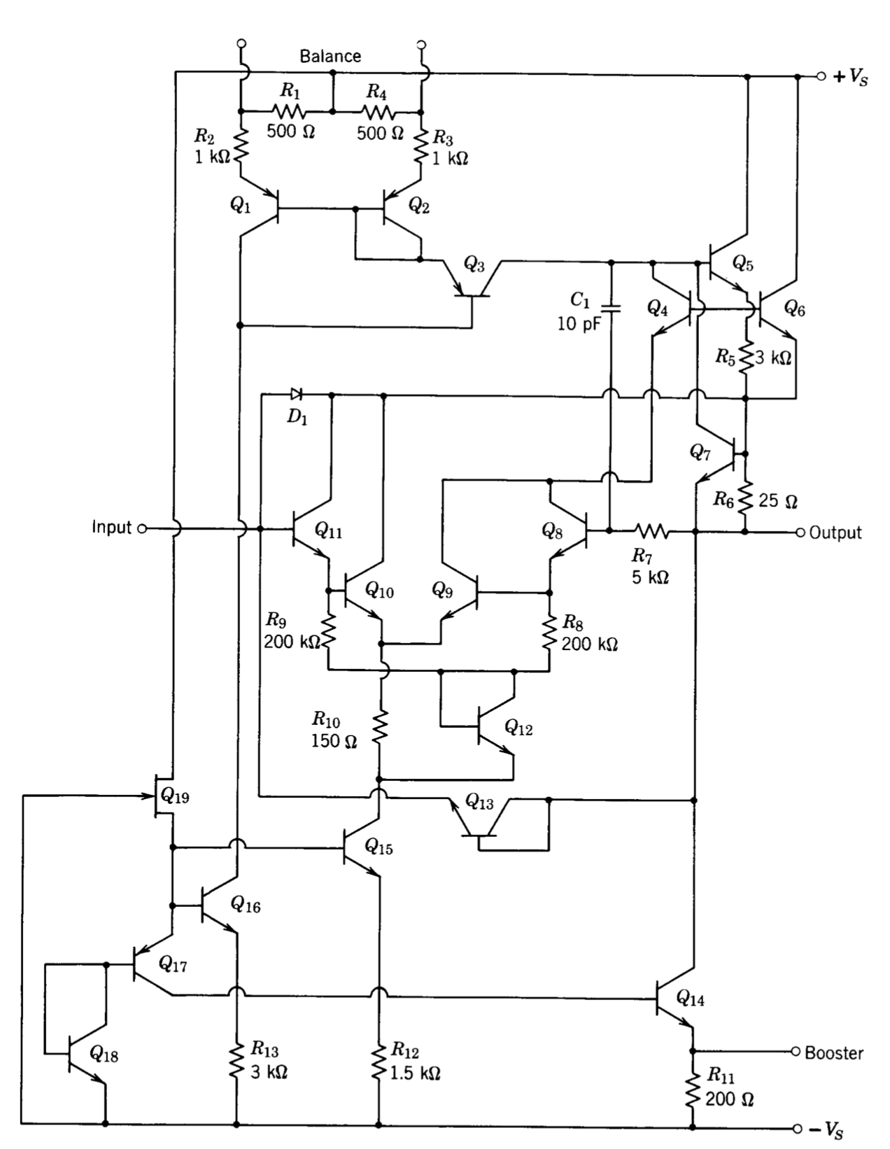
Table 10.4 LM110 Specifications: Electrical Characteristics
| Parameter | Conditions | Min | Typ | Max | Units |
| Input offset voltage | \(T_A = 25^{\circ} C\) | 1.5 | 4.0 | \(mV\) | |
| Input bias current | \(T_A = 25^{\circ} C\) | 1.0 | 3.0 | \(nA\) | |
| Input resistance | \(T_A = 25^{\circ} C\) | \(10^{10}\) | \(10^{12}\) | \(\Omega\) | |
| Input capacitance | 1.5 | \(pF\) | |||
| Large-signal voltage gain | \(T_A = 25^{\circ} C, V_S = \pm 15\ V\) \(V_{\text{out}} = \pm 10\ V, R_L = 8\ k\Omega\) |
0.999 | 0.9999 | \(V/V\) | |
| Output resistance | \(T_A = 25^{\circ} C\) | 0.75 | 2.5 | \(\Omega\) | |
| Supply current | \(T_A = 25^{\circ} C\) | 3.9 | 5.5 | \(mA\) | |
| Input offset voltage | 6.0 | \(mV\) | |||
| Offset voltage | \(-55^{\circ} C \le T_A \le 85^{\circ} C\) | 6 | \(\mu V/^{\circ} C\) | ||
| temperature drift | \(T_A = 125^{\circ} C\) | 12 | \(\mu V/^{\circ} C\) | ||
| Input bias current | 10 | \(nA\) | |||
| Large-signal voltage gain | \(V_S = \pm 15\ V, V_{\text{out}} = \pm 10\ V\) \(R_L = 10\ K\Omega\) |
0.999 | \(V/V\) | ||
| Output voltage swing | \(V_S = \pm 15\ V, R_L = 10\ k\Omega\) | \(\pm 10\) | \(V\) | ||
| Supply current | \(T_A = 125^{\circ} C\) | 2.0 | 4.0 | \(mA\) | |
| Supply-voltage rejection ratio | \(5\ V \le V_S \le 18\ V\) | 70 | 80 | \(dB\) |
The LM 110 voltage follower (Figure 10.23) is an integrated-circuit operational amplifier that elaborates on the one-stage topology described above. Perfomance specifications are listed in Table 10.4. Note that this circuit, like the LM108, uses both super \(\beta\) (narrow base) and conventional (wide base) NPN transistors. The input stage consists of transistors \(Q_8\) through \(Q_{11}\) connected as a differential amplifier using two modified Darlington pairs. Pinch resistors \(R_8\) and \(R_9\) increase the emitter current of \(Q_8\) and \(Q_{11}\) to reduce voltage drift. (See Section 7.4.4 for a discussion of the drift that can result from a conventional Darlington connection.) Transistor \(Q_{15}\) supplies the operating current for the input stage. Transistor \(Q_{16}\) supplies one-half of this current (the nominal operating current of either side of the differential pair) to the current repeater \(Q_1\) through \(Q_3\) that functions as the first-stage load.
Transistors \(Q_5\) and \(Q_6\) form a Darlington emitter follower that isolates the high-resistance node from loads applied to the amplifier. The emitter of \(Q_6\), which is at approximately the output voltage, is used to bootstrap the collector voltage of the \(Q_{10}-Q_{11}\) pair. The resultant operation at nominally zero collector-to-base voltage results in negligible leakage current from \(Q_{11}\). The \(Q_8-Q_9\) pair is cascoded with transistor \(Q_4\). Besides protecting \(Q_8\) and \(Q_9\) from excessive voltages, the cascode results in higher open-loop voltage gain from the circuit.
Diode \(D_1\) and diode-connected transistor \(Q_{13}\) limit the input-to-output voltage difference for a large-signal operation to protect the super \(\beta\) transistors and to speed overload recovery. Transistor \(Q_7\) is a current limiter, while \(Q_{14}\) functions as a current-source load for the output stage. The single-ended emitter follower is used in preference to a complementary
connection since it is more linear and thus better suited to high-frequency applications. An interesting feature of the design is that the magnitude of the current-source load for the emitter follower can be increased by shunting resistor Ru via external terminals. This current can be increased when it is necessary for the amplifier to supply substantial negative output current. The use of boosted output current also increases the power consumption of the circuit, raises its temperature, and can reduce input current because of the increased current gain of transistor \(Q_{11}\) at elevated temperatures.
The capacitive feedback from the collector of \(Q_4\) to the base of \(Q_8\) stabilizes the amplifier. Since the relative potentials are constrained under normal operating conditions, a diode can be used for the capacitor.
The small-signal bandwidth of the LM110 is approximately 20 MHz. This bandwidth is possible from an amplifier produced by the six-mask process because, while lateral PNP's are used for biasing or as static current sources, none are used in the signal path.
It is clear that special designs to improve performance can often be employed if the intended applications of an amplifier are constrained. Unfortunately, most special-purpose designs have such limited utility that fabrication in integrated-circuit form is not economically feasible. The LM110 is an example of a circuit for which such a special design is practical, and it provides significant performance advantages compared to general-purpose amplifiers connected as followers.
Recent Developments
The creativity of the designers of integrated circuits in general and monolithic operational amplifiers in particular seems far from depleted. Innovations in processing and circuit design that permit improved performance occur with satisfying regularity. In this section some of the more promising recent developments that may presage exciting future trends are described.
The maximum closed-loop bandwidth of most general-purpose monolithic operational amplifiers made by the six-mark process is limited to approximately 1 MHz by the phase shift associated with the lateral-PNP transistors used for level shifting. While this bandwidth is more than adequate for many applications, and in fact is advantageous in some because amplifiers of modest bandwidth are significantly more tolerant of poor decoupling, sloppy layout, capacitive loading, and other indiscretions than are faster designs, wider bandwidth always extends the application spectrum. Since it is questionable if dramatic improvements will be made in the frequency response of process-compatible PNP transistors in the near future, present efforts to extend amplifier bandwidth focus on eliminating the lateral PNP's from the gain path, at least at high frequencies.
One possibility is to capacitively bypass the lateral PNP's at high frequencies. This modification can be made to an LM101 or LM101A by connecting a capacitor from the inverting input to terminal 1 (see Figs. 10.17 and 10.19). The capacitor provides a feedforward path (see Section 8.2.2) that bypasses the input-stage PNP transistors. Closed-loop bandwidths on the order of 5 MHz are possible, and this method of compensation is discussed in greater detail in a later section. Unfortunately, feedforward does not improve the amplifier speed for signals applied to the noninverting input, and as a result wideband differential operation is not possible.
The LM 118 pioneered a useful variation on this theme. This operational amplifier is a three-stage design including an NPN differential input stage, an intermediate stage of lateral PNP's that provides level shifting, and a final NPN voltage-gain stage. The intermediate stage is capacitively by-passed, so that feedforward around the lateral-PNP stage converts the circuit to a two-stage NPN design at high frequencies, while the PNP stage provides the gain and level shifting required at low frequencies. Since the feedforward is used following the input stage, full bandwidth differential operation is retained. Internal compensation insures stability with direct feedback from the output to the inverting input and results in a unity-gain frequency of approximately 15 MHz and a slew rate of at least 50 volts per microsecond. External compensation can be used for greater relative stability.
A second possibility is to use the voltage drop that a current source produces across a resistor for level shifting. It is interesting to note that the \(\mu A702\), the first monolithic operational amplifier that was designed before the advent of lateral PNP's, uses this technique and is capable of closed-loop bandwidths in excess of 20 MHz. However, the other performance specifications of this amplifier preclude its use in demanding applications. The \(\mu A715\) is a more modern amplifier that uses this method of level shifting. It is an externally compensated amplifier capable of a closed-loop bandwidth of approximately 20 MHz and a slew rate of \(100\ V/\mu s\) in some connections.
It is evident that improved high-speed amplifiers will evolve in the future. The low-cost availability of these designs will encourage the use of circuits such as the high-speed digital-to-analog converters that incorporate them.
A host of possible monolithic operational-amplifier refinements may stem from improved thermal design. One problem is that many presently available amplifiers have a d-c gain that is limited by thermal feedback on the chip. Consider, for example, an amplifier with a d-c open-loop gain of \(10^5\), so that the input differential voltage required for a 10-volt output is \(100\ \mu V\). If the thermal gradient that results from the 10-volt change in output level changes the input-transistor pair temperature differentially
by \(0.05^{\circ}\ C\) (a real possibility, particularly if the output is loaded), differential input voltage is dominated by thermal feedback rather than by limited d-c gain. Several modern instrumentation amplifiers use sophisticated thermal-design techniques such as multiple, parallel-connected input transistors located to average thermal gradients and thus allow usable gains in the range of \(10^6\). These techniques should be incorporated into general-purpose operational amplifiers in the future.
An interesting method of output-transistor protection was originally developed for several monolithic voltage regulators, and has been included in the design of at least one high-power monolithic operational amplifier. The level at which output current should be limited in order to protect a circuit is a complex function of output voltage, supply voltage, the heat sink used, ambient temperature, and the time history of these quantities because of the thermal dynamics of the circuit. Any limit based only on output current level (as is true with most presently available operational amplifiers) must be necessarily conservative to insure protection. An attractive alternative is to monitor the temperature of the chip and to cut off the output before this temperature reaches destructive levels. As this technique is incorporated in more operational-amplifier designs, both output current capability and safety (certain present amplifiers fail when the output is shorted to a supply voltage) will improve. The high pulsed-current capability made possible by thermal protection would be particularly valuable in applications where high-transient capacitive changing currents are encountered, such as sample-and-hold circuits.
Another thermal-design possibility is to include temperature sensors and heaters on the chip so that its temperature can be stabilized at a level above the highest anticipated ambient value. This technique has been used in the \(\mu A726\) differential pair and \(\mu A727\) differential amplifier. Its inclusion in a general-purpose operational-amplifier design would make parameters such as input current and offset independent of ambient temperature fluctuations.