
10.5: ADDITIONS TO IMPROVE PERFORMANCE
- Page ID
- 74649

Operational amplifiers are usually designed for general-purpose applicability. For this reason and because of limitations inherent to integrated-circuit fabrication, the combination of an integrated-circuit operational amplifier with a few discrete components often tailors performance advantageously for certain applications. The use of customized compensation networks gives the designer a powerful technique for modifying the dynamics of externally compensated operational amplifiers. This topic is discussed in Chapter 13. Other frequently used modifications are intended to improve either the input-stage or the output-stage characteristics of monolithic amplifiers, and some of these additions are mentioned in this section.
One advantage that many discrete-component operational amplifiers have compared with some integrated-circuit designs is lower input current. This improvement usually results because the input current of the discrete- component design is compensated by one of the techniques described in Section 7.4.2. These techniques can reduce the input current of discrete-component designs, particularly at one temperature, to very low levels. The same techniques can be used to lower the input current of integrated-circuit amplifiers. Many amplifiers can be well compensated using transistors as shown in Figure 7.14. Transistor types, such as the 2N4250 or 2N3799, which have current-gain versus temperature characteristics similar to those of the input transistors of many amplifiers, should be used.
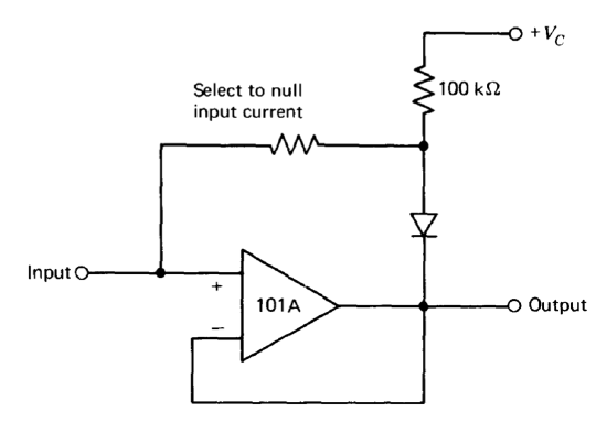
The connection shown in Figure 10.24 can be used to reduce the input current of a follower-connected LMl0lA. As a consequence of the temperature-dependent input-stage operating current of this amplifier (see Section 10.4.1), the temperature coefficient of its input current is approximately 0.3% per degree Centigrade, comparable to that of a forward- biased silicon diode at room temperature.
Another possibility involves the use of the low input current LM110 as a preamplifier for an operational amplifier. Since the bandwidth of the LM110 is much greater than that of most general-purpose operational amplifiers, feedback-loop dynamics are unaffected by the addition of the preamplifier. While this connection increases voltage drift, the use of self heating (see Section 10.4.4) and simple input current compensation can result in an input current under \(0.5\ nA\) over a wide temperature range.(While the LM108 has comparably low input current, its dynamics and load-driving capability are inferior to those of many other general-purpose amplifiers. As a result the connection described here is advantageous in some applications.)
Field-effect transistors(While the best-matched field-effect transistors are made by a monolithic process, the process cannot simultaneously fabricate high-quality bipolar transistors. Some manufacturers offer hybrid integrated circuits that combine two chips in one package to provide a FET-input operational amplifier. The \(\mu A740\) is a monolithic FET-input amplifier, but its performance is not as good as that of the hybrids.) can be connected as source followers in front of an operational amplifier as shown in Figure 10.25. Input current of a fraction of a nA at moderate temperatures is obtained at the expense of increased drift and poorer common-mode rejection ratio. The use of relatively inex pensive dual field-effect transistors yields typical drift figures of 10 to 100 pV,/C. The product of source-follower output resistance and amplifier input capacitance is normally small enough so that dynamics remain unchanged. If this capacitive loading is a problem, the gate and source terminals of the FET's can be shunted with small capacitors.
It is possible to reduce the drift of an operational amplifier by preceding it with a differential-amplifier stage, since the drift of a properly designed discrete-component differential amplifier can be made a fraction of a microvolt per degree Centigrade (see Chapter 7). This method is most effective when relatively high voltage gain is obtained from the differential stage and when its operating current is high compared with the input current of the operational amplifier. A recently developed integrated circuit (the LM121) is also intended to function as a preamplifier for operational amplifiers. The bias current of this preamplifier can be adjusted, and combined drift of less than one microvolt per degree Centigrade is possible. The use of a preamplifier that provides voltage gain often complicates compensation because the increased loop transmission that results may compromise stability in some applications.
The output current obtainable from an integrated-circuit operational amplifier is limited by the relatively small geometry of the output transistors and by the low power dissipation of a small chip. These limitations can be overcome by following the amplifier with a separate output stage.
There is a further significant performance advantage associated with the use of an external output stage. If output current is supplied from a transistor included on the chip, the dominant chip power dissipation is that associated with load current when currents in excess of several milliamperes are supplied. As a consequence, chip temperature can be strongly dependent on output voltage level. As mentioned earlier, thermal feedback to the input transistors deteriorates performance because of associated drift and input current changes. A properly designed output stage can isolate the amplifier from changes in load current so that chip temperature becomes virtually independent of output voltage and current.
Output-stage designs of the type described in Section 8.4 can be used. The wide bandwidth of emitter-follower circuits normally does not compromise frequency response. The output stage can be a discrete-component design, or any of several monolithic or hydrid integrated circuits may be used. The MC1538R is an example of a monolithic circuit that can be used as a unity-gain output buffer for an operational amplifier. This circuit is housed in a relatively large package that permits substantial power dissipation, and can provide output currents as high as \(300\ mA\). Its bandwidth exceeds 8 MHz, considerably greater than that of most general-purpose operational amplifiers.
Another possibility in low output power situations is to use a second operational amplifier connected as a noninverting amplifier (gains between 10 and 100 are commonly used) as an output stage for a preceding operational amplifier. Advantages include the open-loop gain increase provided by the noninverting amplifier, and virtual elimination of thermal-feedback problems since the maximum output voltage required from the first amplifier is the maximum output voltage of the combination divided by the closed-loop gain of the noninverting amplifier. It is frequently necessary to compensate the first amplifier very conservatively to maintain stability in feedback loops that use this combination.
PROBLEMS
Exercise \(\PageIndex{1}\)
You are the president of Single-Stone Semiconductor, Inc. Your best-selling product is a general-purpose operational amplifier that has chip dimensions of 0.05 inch square. Experience shows that you make a satisfactory profit if you sell your circuits at a price equal to 10 times the cost at the wafer level. You presently fabricate your circuits on wafers with a usable area of 3 square inches. The cost of processing a single wafer is $40, and yields are such that you currently sell your amplifier for one dollar. Your chief engineer describes a new amplifier that he has designed. It has characteristics far superior to your present model and can be made by the same process, but it requires a chip size of 0.05 inch by 0.1 inch. Explain to your engineer the effect this change would have on selling price. You may assume that wafer defects are randomly distributed.
Exercise \(\PageIndex{2}\)
A current repeater of the type shown in Figure 10.9 is investigated with a transistor curve tracer. The ground connection in this figure is connected to the curve-tracer emitter terminal, the input is connected to the base terminal of the tracer, and the repeater output is connected to the collector terminal of the curve tracer. Assume that both transistors have identical values for \(I_S\) and very high current gain. Draw the type of a display you expect on the curve tracer.
Exercise \(\PageIndex{3}\)
Assume that it is possible to fabricate lateral-PNP transistors with a current gain of 100 and a value of \(C_{\pi}\) equal to \(400\ pF\) at \(100\ \mu A\) of collector current. A unity-gain current repeater is constructed by bisecting the collector of one of these transistors and connecting the device as shown in Figure 10.10. Calculate the 0.707 frequency of the current transfer function for this structure operating at a total collector current of \(100\ \mu A\). You may neglect \(C_{\mu}\) and base resistance for the transistor. Contrast this value with the frequency at which the current gain of a single-collector lateral-PNP transistor with similar parameters drops to 0.707 of its low-frequency value.
Exercise \(\PageIndex{4}\)
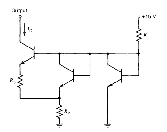
Figure 10.26 shows a connection that can be used as a very low level current source. Assume that all transistors have identical values of \(I_S\), high \(\beta\), and are at a temperature of \(300^{\circ} K\). Find values for \(R_1, R_2\), and \(R_3\) such that the output current will be \(1\ \mu A\) subject to the constraint that the sum of the resistor values is less than \(100\ k\Omega\).
Exercise \(\PageIndex{5}\)
Consider the three current repeater structures shown in Figs. 10.9, 10.11\(a\), and 10.11\(b\). Assume perfectly matched transistors, and calculate the incremental output resistance of each connection in terms of \(\beta\) and \(\eta\) of the transistors and the operating current level.
Exercise \(\PageIndex{6}\)
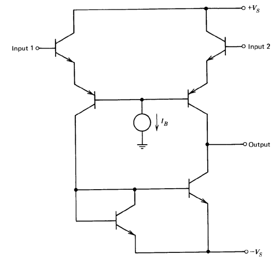
The final voltage-gain stage and output buffer of an integrated-circuit operational amplifier is shown in Figure 10.27. Calculate the quiescent collector-current level of the complementary emitter follower. You may assume that the current gain of the NPN transistors is 100, while that of PNP'S is 10. You may further assume that all NPN's have identical characteristics, as do all PNP'S.
Exercise \(\PageIndex{7}\)
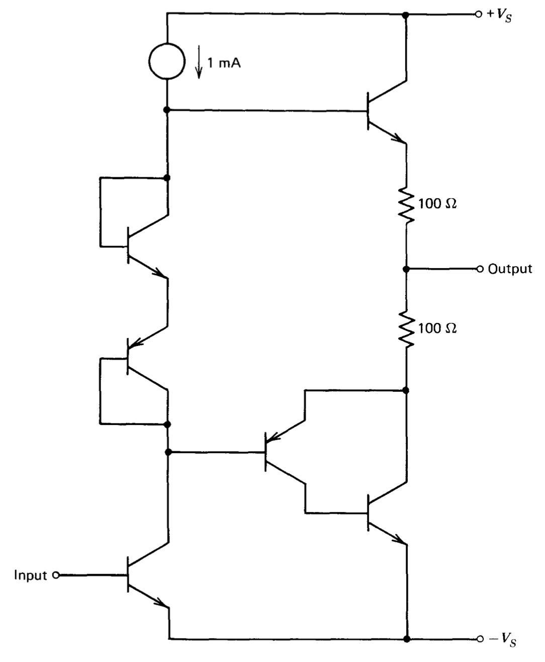
An operational amplifier input stage is shown in Figure 10.28. Calculate the drift referred to the input of this amplifier attributable to changes in current gain of the transistors used in the current repeater. You may assume that these transistors are perfectly matched, have a common-emitter current gain of 100, and a fractional change in current gain of 0.5% per degree Centigrade. Suggest a circuit modification that reduces this drift.
Exercise \(\PageIndex{8}\)
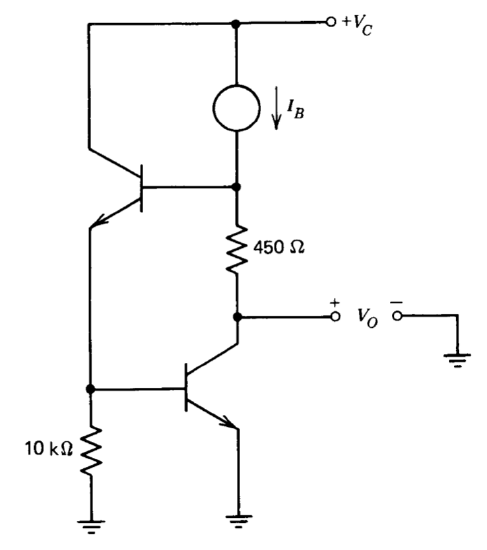
A portion of the biasing circuitry of the LM101A operational amplifier is shown in Figure 10.29. This circuit has the interesting property that for a properly choosen operating current level, the bias voltage is relatively insensitive to changes in the current level. Determine the value of \(I_B\) that makes \(\partial V_O/\partial I_B\) zero. You may assume high current gain for both transistors.
Exercise \(\PageIndex{9}\)
Determine how unity-gain frequency and slew rate are related to the first-stage bias current for the \(\mu A776\) operational amplifier. Use the specifications for this amplifier to estimate input-stage quiescent current at a set-current value of \(1.5\ \mu A\). Assuming that the ratio of bias current to set current remains constant for lower values of set current, estimate the 10 to 90% rise time in response to a step for the \(\mu A776\) connected as a non-inverting gain-of-ten amplifier at a set current of \(1\ nA\). Also estimate slew rate and power consumption for the \(\mu A776\) at this set current.
Exercise \(\PageIndex{10}\)
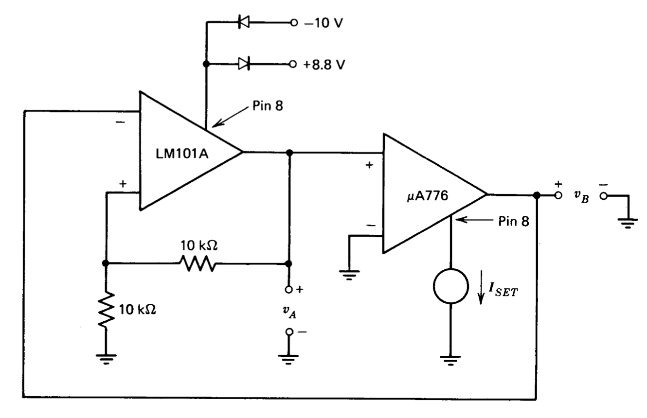
A \(\mu A776\) is connected in a loop with a LM101A as shown in Figure 10.30.
(a) Show that this is one way to implement a function generator similar to that described in Section 6.3.3.
(b) Plot the transfer characteristics of the LM101A with feedback (i.e., the voltage \(v_A\) as a function of \(v_B\)).
(c) Draw the waveforms \(v_A(t)\) and \(v_B(t)\) for this circuit. You may assume that the slew rate of the 101A is much greater than that of the \(\mu A776\).
(d) How do these waveforms change as a function of \(I_{SET}\)?
Exercise \(\PageIndex{11}\)
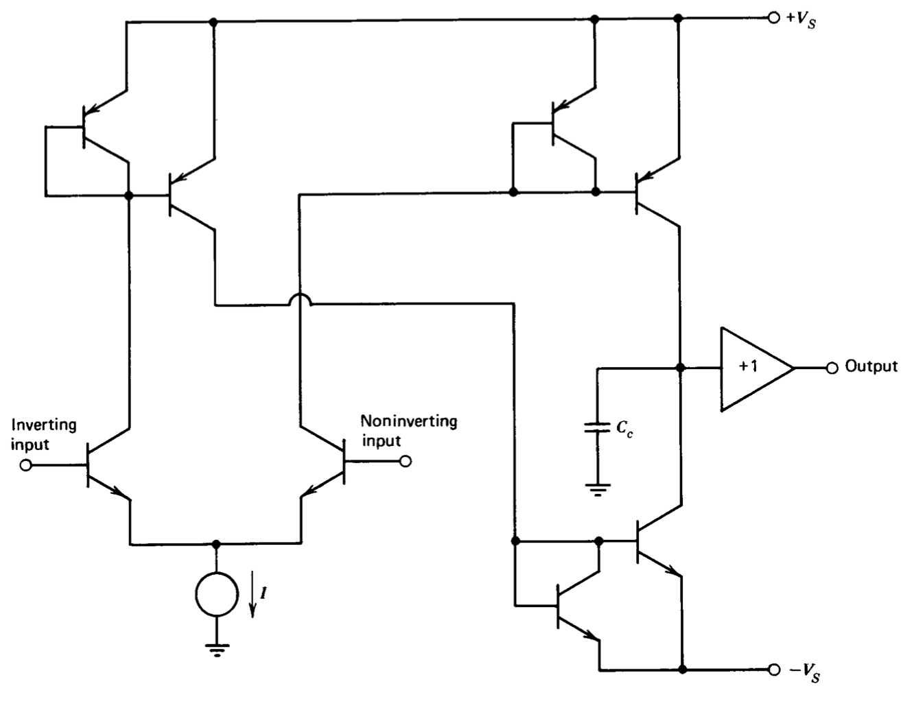
A simplified schematic of an operational amplifier is shown in Figure 10.31.
(a) How many stages has this amplifier?
(b) Make the (probably unwarranted) assumption that all transistors have identical (high) values for \(\beta\) and identical values for \(\eta\). Further assume that appropriate pairs have matched values of \(I_S\). Calculate the low-frequency gain of the amplifier.
(c) Calculate the amplifier unity-gain frequency and slew rate as a function of the current \(I\), the capacitor \(C_c\), and any other quantities you need. You may assume that this capacitor dominates amplifier dynamics.
(d) Suggest a circuit modification that retains essential features of the amplifier performance, yet increases its low-frequency voltage gain.
Exercise \(\PageIndex{12}\)
Specifications for the LM101A operational amplifier indicate a maximum input bias current of \(100\ nA\) and a maximum temperature coefficient of input offset current (input offset current is the difference between the bias current required at the two amplifier inputs) of \(0.2\ nA\) per degree Centigrade. These specifications apply over a temperature range of \(-55^{\circ} C\) to \(+ 125^{\circ} C\). Our objective is to precede this amplifier with a matched pair of 2N5963
transistors connected as emitter followers so that it can be used in applications that require very low input currents. Assume that you are able to match pairs of 2N5963 transistors so that the difference in base-to-emitter voltages of the pair is less than \(2\ mV\) at equal collector currents. Design an emitter-follower circuit using one of these pairs and any required bias-circuit components with the following characteristics:
1. The bias current required at the input of the emitter followers is relatively independent of common-mode level over the range of \(\pm 10\) volts.
2. The drift referred to the input added to the complete circuit by the emitter followers is less than \(\pm 2\ \mu V\) per degree Centigrade. Indicate how you plan to balance the emitter-follower pair in conjunction with the amplifier to achieve this result.
Estimate the input current for the modified amplifier with your circuit, assuming that the common-emitter current gain of the 2N5963 is 1000. Estimate the differential input resistance of the modified amplifier. You will probably need to know the differential input resistance of the LM101A to complete this calculation. In order to determine this quantity, show that for the LM101A input-stage topology, differential input resistance can be determined from input bias current alone.