
11.2: SPECIFICATIONS
- Page ID
- 58474

A firm understanding of some of the specifications used to describe operational amplifiers is necessary to determine if an amplifier will be satisfactory in an intended application. Unfortunately, completely specifying a
complex circuit is a virtually impossible task. The problem is compounded by the fact that not all manufacturers specify the same quantities, and not all are equally conservative with their definitions of "typical," "maximum," and "minimum." As a result, the question of greatest interest to the de signer (will it work in my circuit?) is often unanswered.
Definitions
Some of the more common specifications and their generally accepted definitions are listed below. Since there are a number of available operational amplifiers that are not intended for differential operation (e.g., amplifiers that use feedforward compensation are normally single-input amplifiers), the differences in specifications between differential- and single-input amplifiers are indicated when applicable.
Input offset voltage. The voltage that must be applied between inputs of a differential-input amplifier, or between the input and ground of a single- input amplifier, to make the output voltage zero. This quantity may be specified over a given temperature range, or its incremental change (drift) as a function of temperature, time, supply voltage, or some other parameter may be given.
Input bias current. The current required at the input of a single-input amplifier, or the average of the two input currents for a differential-input amplifier.
Input offset current. The difference between the two input currents of a differential-input amplifier. Both offset and bias current are defined for zero output voltage, but in practice the dependence of these quantities on output voltage level is minimal. The dependence of these quantities on temperature or other operating conditions is often specified.
Common-mode rejection ratio. The ratio of differential gain to common-mode gain.
Supply-voltage sensitivity. The change in input offset voltage per unit change in power-supply voltage. The reciprocal of this quantity is called the supply-voltage rejection ratio.
Input common-mode range. The common-mode input signal range for which a differential amplifier remains linear.
Input differential range. The maximum differential signal that can be applied without destroying the amplifier.
Output voltage range. The maximum output signal that can be obtained without significant distortion. This quantity is usually specified for a given load resistance.
Input resistance. Incremental quantities are normally specified for both differential (between inputs) and common-mode (either input to ground) signals.
Output resistance. Incremental quantity measured without feedback unless otherwise specified.
Voltage gain or open-loop gain. The ratio of the change in amplifier out put voltage to its change in input voltage when the amplifier is in its linear region and when the input signal varies extremely slowly. This quantity is frequently specified for a large change in output voltage level.
Slew rate. The maximum time rate of change of output voltage. This quantity depends on compensation for an externally compensated amplifier. Alternatively, the maximum frequency at which an undistorted given amplitude sinusoidal output can be obtained may be specified.
Bandwidth specifications. The most complete specification is a Bode plot, but unfortunately one is not always given. Other frequently specified quantities include unity-gain frequency, rise time for a step input or half-power frequency for a given feedback connection. Most confusing is a gain-bandwidth product specification, which may be the unity-gain frequency, or may be the product of closed-loop voltage gain and half-power bandwidth in some feedback connection.
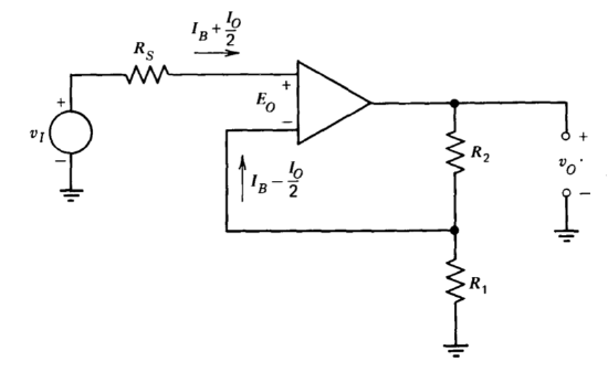
Even when operational-amplifier specifications are supplied honestly and in reasonable detail, the prediction of the performance of an amplifier in a particular connection can be an involved process. As an example of this type of calculation, consider the relatively simple problem of finding the output voltage of the noninverting amplifier connection shown in Figure 11.1 when \(v_I = 0\). The voltage offset of the amplifier is equal to \(E_O\). It is assumed that the low-frequency voltage gain of the amplifier ao is very large so that the voltage between the input terminals of the amplifier is nearly equal to \(E_O\). (Recall that with \(E_O\) applied to the input terminals, \(v_O = 0\). If \(a_0\) is very large, any other d-c output voltage within the linear region of the amplifier can be obtained with a voltage of approximately \(E_O\) applied between inputs.) The currents at the amplifier input terminals expressed in terms of the bias current \(I_B\) and the offset current \(I_O\) are also shown in this figure.(The specification of the input currents in terms of bias and offset current does not, of course, indicate which input-terminal current is larger for a particular amplifier. It has been arbitrarily assumed in Figure 11.1 that the offset current adds to the bias current at the noninverting input and subtracts from it at the inverting input.)
The voltage and current values shown in the figure imply that, for \(v_I = 0\),
\[-R_S \left (I_B + \dfrac{I_O}{2} \right ) - v_O \left ( \dfrac{R_1}{R_1 + R_2} \right ) + \left (I_B - \dfrac{I_O}{2} \right ) \dfrac{R_1 R_2}{R_1 + R_2} = E_O \nonumber \]
Solving for \(V_O\) yields
\[v_O = -\dfrac{(R_2 + R_1)}{R_1} E_O - \left (\dfrac{R_1 + R_2}{R_1} \right ) R_S \left (I_B + \dfrac{I_O}{2} \right ) + R_2 \left (I_B - \dfrac{I_O}{2} \right )\label{eq11.2.2} \]
This equation shows that the output voltage attributable to amplifier input current can be reduced by scaling resistance levels, but that the error resulting from voltage offset is irreducible since the ratio \((R_1 + R_2)/R_1\) presumably must be selected on the basis of the required ideal closed-loop gain. Equation \(\ref{eq11.2.2}\) also demonstrates the well-known result that balancing the resistances connected to the two inputs eliminates offsets attributable to input bias current, since with \(R_1 R_2/(R_1 + R_2) = R_S\), the output voltage is independent of \(I_B\).
As another example of the use of amplifier specifications, consider a device with an offset \(E_O\), a d-c gain of \(a_0\), and a maximum output voltage \(V_{OM}\). The maximum differential input voltage required in order to obtain any static output voltage within the dynamic range of the amplifier is then(The quantities in the equation are assumed to be maximum magnitudes. The possibility of cancellation because of algebraic signs exists for only one polarity of output voltage, and is thus ignored when calculating the maximum magnitude of the input voltage.)
\[V_{IM} = E_O + \dfrac{V_{OM}}{a_0} \nonumber \]
This equation shows that values of ao in excess of \(V_{OM}/E_O\) reduce the amplifier input voltage (which must be low for the closed-loop gain to approximate its ideal value) only slightly. We conclude that if \(a_0 > V_{OM}/E_O\), further operational-amplifier design efforts are better devoted to lowering offset rather than to increasing \(a_0\).
Parameter Measurement
One way to bypass the conspiracy of silence that often surrounds amplifier specifications is to measure the parameters that are important in a particular application. Measurement allows the user to determine for himself how a particular manufacturer defines "typical," "maximum," and "minimum," and also permits him to grade circuits so that superior units can be used in the more demanding applications.
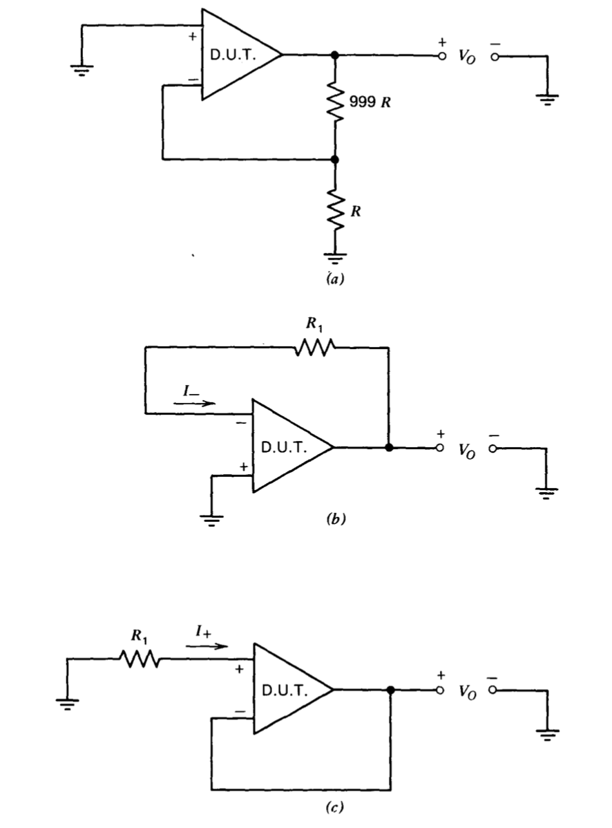
The d-c characteristics exclusive of open-loop gain are relatively straight forward to measure. Circuits that can be used to measure the input offset voltage \(E_O\) and the input currents at the two input terminals, \(I_{+}\) and \(I_{-}\), are shown in Figure 11.2. In the circuit of Figure 11.2\(a\), assume that resistor values are chosen so that \(|E_O| gg |I_R|\). The quiescent voltages are
\[(-10^{-3} V_O + E_O)a_0 = V_O \nonumber \]
for an appropriately chosen reference polarity for \(E_O\). Solving this equation for \(V_O\) yields
\[V_O = \dfrac{a_0 E_O}{1 + 10^{-3} a_0} \simeq 10^3 E_O \nonumber \]
Thus we see that this circuit uses the amplifier to raise its own offset voltage to an easily measured level.
If the resistor \(R_1\) in Figs. 11.2\(b\) and 11.2\(c\) is chosen so that both \(|I_{-} R_1|\) and \(|I_{+} R_1|\gg |E_O|\), the output voltages are
\[V_O = I_{-} R_1 \nonumber \]
and
\[V_O = -I_{+} R_1 \nonumber \]
respectively. The measurement of \(I_{-}\) and \(I_{+}\) allows direct calculation of offset and bias currents, since we recall from earlier definitions that the bias current is equal to the average of \(I_{+}\) and \(I_{-}\), while the offset current is equal to the magnitude of the difference between these two quantities.
A test box that includes a socket for the device under test and incorporates mode switching to select among the tests is easily constructed. Results can be displayed on an inexpensive D'Arsonval meter movement, since resistor values can be chosen to yield output voltages on the order of one volt. The low-pass characteristics of the meter movement provides a degree of noise rejection that improves the accuracy of the measurements. If further noise filtering is required, moderate-value capacitors may be used in parallel with resistors \(999R\) and \(R_1\) in Figure 11.2.
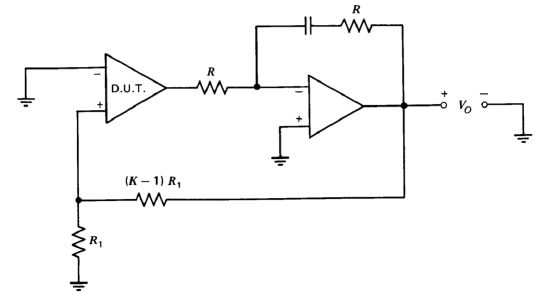
The offset measurement circuit shown in Figure 11.2\(a\) requires large loop-transmission magnitude for proper operation. If there is the possibility that the low-frequency loop transmission of a particular amplifier is too small, the alternative circuit shown in Figure 11.3 can be used to measure offset. The second amplifier provides very large d-c gain with the result that the voltage out of the amplifier under test is negligible. At moderate frequencies, the second amplifier functions as a unity-gain inverter so that loop stability is not compromised by the integrator characteristics that result if the feedback resistor \(R\) is eliminated. Lowering the value of this
feedback resistor relative to the input resistor of the second amplifier may improve stability, particularly when the \((K - 1)R_1\) resistor is bypassed for noise reduction. Since this connection keeps the output voltage from the amplifier under test near ground, \(V_O\) will be (in the absence of input-current effects) simply equal to \(KE_O\).
The supply-voltage rejection ratio of an amplifier can be measured with the same circuitry used to measure offset if provision is included to vary voltages applied to the amplifier. The supply-voltage rejection ratio is defined as the ratio of a change in supply voltage to the resulting change in input offset voltage.
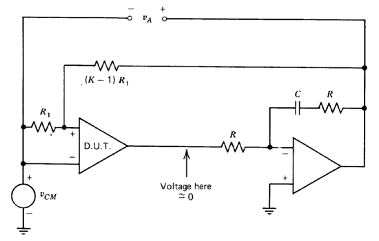
The technique of including a second amplifier to increase loop transmission simplifies the measurement of common-mode rejection ratio (see Figure 11.4). If the differential gain \(a_0\) of the amplifier is large compared to its common-mode gain \(a_{cm}\), we can write
\[0 = a_{cm} v_{CM} + \dfrac{a_0 v_A}{K} \nonumber \]
Thus
\[\left | \dfrac{a_0}{a_{cm}} \right | = \text{CMRR} = \left | \dfrac{Kv_{CM}}{v_A} \right |
Since the voltage \(v_A\) also includes a component proportional to the offset voltage of the amplifier, it may be necessary to use incremental measurements to determine accurately rejection ratio.
The slew rate of an amplifier may be dependent on the time rate of change of input-signal common-mode level and will be a function of compensation for an amplifier with selectable compensation. Standardized results that allow intercomparison of various amplifiers can be obtained by connecting the amplifier as a unity-gain inverter and applying a step input that sweeps the amplifier output through most of its dynamic range. Diode clamping at the inverting input of the amplifier can be used to prevent large common-mode signals. (See Section 13.3.7 for a representative circuit.) Alternatively, the maximum slew rate in a specific connection of interest can often be determined by applying a large enough input signal to force the maximum time rate of change of amplifier output voltage.
The open-loop transfer function of an amplifier is considerably more challenging to measure. Consider, for example, the problem of determining d-c gain. We might naively assume that the amplifier could be operated open loop (after all, we are measuring open-loop gain), biased in its linear region by applying an appropriate input quiescent level, and gain determined by adding an incremental step at the input and measuring the change in output level. The hazards of this approach are legion. The output signal is normally corrupted by noise and drift so that changes are difficult to determine accurately. We may also find that the amplifier exhibits bistable behavior, and that it is not possible to find a value for input voltage that forces the amplifier output into its linear region. This phenomenon results from positive thermal feedback in an integrated circuit, and can also occur in discrete designs because of self-heating, feedback through shared bias networks or power supplies, or for other reasons. The positive feedback
that leads to this behavior is swamped by negative feedback applied around the amplifier in normal applications, and thus does not disturb performance in the usual connections.
After some frustration it is usually concluded that better results may be obtained by operating the amplifier in a closed-loop connection. Signal amplitudes can be adjusted for the largest output that insures linear performance at some frequency, and the corresponding input signal measured. The magnitude and angle of the transfer function can be obtained if the input signal can be accurately determined. Unfortunately, the signal at the amplifier input is usually noisy, particularly at frequencies where the open-loop gain magnitude is large. A wave analyzer or an amplifier followed by a phase-sensitive demodulator driven at the input frequency may be necessary for accurate measurements. This technique can even be used to determine \(a_0\) if the amplifier is compensated so that the first pole in its open-loop transfer function is located within the frequency range of the detector.
There are also indirect methods that can be used to approximate the open-loop transfer function of the amplifier. The small-signal closed-loop frequency or transient response can be measured for a number of different values of frequency-independent feedback \(f_0\). A Nichols chart or the curves of Figure 4.26 may then be used to determine important characteristics of \(a(j\omega )\) at frequencies near that for which \(|a(j\omega )f_0 = 1\). Since various values offo are used, \(a(j\omega )\) can be determined at several different frequencies. This type of measurement often yields sufficient information for use in stability calculations.
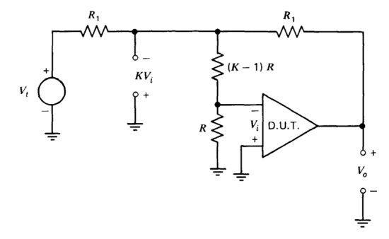
A third possibility is to test the amplifier in a connection that provides a multiple of the signal at the amplifier input, in much the same way as does the circuit suggested earlier for offset measurement. Figure 11.5 shows one possibility. The signal at the junction of the two resistors labeled \(R_1\) is \(K\) times as large as the input signal applied to the amplifier, and can be compared with either \(V_o\) or \(V_t\) (which is equal to \(-V\), when the loop transmission is large) in order to determine the open-loop transfer function of the amplifier. Note that if the signal at the junction of the two equal-value resistors is compared with \(V_o\), this method does not depend on large loop transmission.
While this method does scale the input signal, it does not provide filtering, with the result that some additional signal processing may be necessary to improve signal-to-noise ratio.