
11.4: REPRESENTATIVE LINEAR CONNECTIONS
- Page ID
- 75049

The objective of many operational-amplifier connections is to provide a linear gain or transfer function between circuit input and output signals. This section augments the collection of linear applications we have seen in preceding sections. As mentioned earlier, our objective in discussing these
circuits is not to form a circuits handbook, but rather to encourage the creativity so essential to useful imaginative designs.
The connections presented in this and subsequent sections do not include the minor details that are normally strongly dependent on the specifics of a particular application and the operational amplifier used, and that would obscure more important and universal features. For example, no attempt is made to balance the resistances facing both input terminals, although we have seen that such balancing reduces errors related to amplifier input
currents. We tacitly assume that the amplifier with feedback provides its ideal closed-loop gain unless specifically mentioned otherwise. Similarly, stability is assumed. The methods used to guarantee the latter assumption are the topic of Chapter 13.
Differential Amplifiers
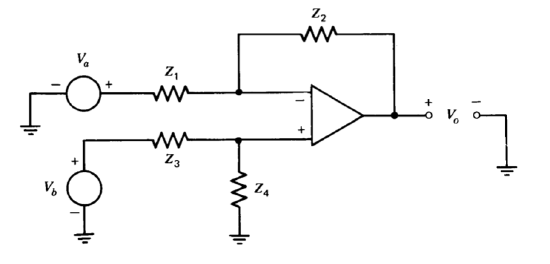
We have seen numerous examples of both inverting and noninverting amplifier connections. Figure 11.10 shows a topology that combines the features of both of these connections. The ideal input-output relationship is easily determined by superposition. If \(V_b\) is zero,
\[V_o = -\dfrac{Z_2}{Z_1} V_a \nonumber \]
If \(V_a\) is zero, the circuit is a noninverting amplifier preceded by an attenuator, and
\[V_o = \left ( \dfrac{Z_4}{Z_3 + Z_4} \right ) \left ( \dfrac{Z_1 + Z_2}{Z_1} \right ) V_b \nonumber \]
Linearity insures that in general
\[V_o = \left ( \dfrac{Z_4}{Z_3 + Z_4} \right ) \left ( \dfrac{Z_1 + Z_2}{Z_1} \right ) V_b - \dfrac{Z_2}{Z_1} V_a \nonumber \]
If values are selected so that \(Z_4/Z_3 = Z_2/Z_1\).
\[V_o = \dfrac{Z_2}{Z_1} (V_b - V_a) \nonumber \]
This connection is frequently used with four resistors to form a differential amplifier. Adjustment of any of the four resistors can be used to zero common-mode gain. Other possibilities involve combining two capacitors for \(Z_2\) and \(Z_4\) with two resistors for \(Z_1\) and \(Z_3\). If the time constants of the two combinations are equal, a differential or a noninverting integrator results.
It is important to note that the input current at the \(V_a\) terminal of the differential connection is dependent on both input voltages, while the current at the \(V_b\) terminal is dependent only on voltage \(V_b\). This nonsymmetrical loading can cause errors in some applications. Two noninverting unity-gain amplifiers can be used as buffers to raise input impedance to very high levels if required.
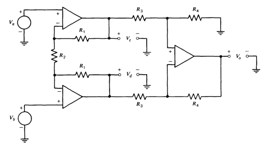
If the design objective is a high-input-impedance differential amplifier with high common-mode rejection ratio, the connection shown in Figure11.11 can be used. Consider a common-mode input signal with \(V_a = V_b = V_i\). In this case the two left-hand amplifiers combine to keep the voltage across \(R_2\) zero. Thus for a common-mode input, the intermediate voltages \(V_c\) and \(V_d\) are related to inputs as
\[V_c = V_d = V_a \ \ \ V_a = V_b \nonumber \]
Alternatively, consider a pure differential input signal with \(V_i/2 = V_a = - V_b\). In this case the midpoint of resistor \(R_2\) is an incrementally grounded point, and each of the left-hand amplifiers functions as a noninverting amplifier with a gain of \((2R_1 + R_2)/R_2\). Linearity insures that the differential gain of the left-hand pair of amplifiers must be independent of common-mode level. Thus
\[\dfrac{V_c - V_d}{V_a - V_b} = \dfrac{2R_1 + R_2}{R_2} \nonumber \]
The right-hand amplifier has a gain of zero for the common-mode component of \(V_c\) and \(V_d\), and a gain of \(R_4/R_3\) for the differential component of these intermediate signals. Combining expressions shows that \(V_o\) is independent of the common-mode component of \(V_a\) and \(V_b\), and is related to these signals as
\[V_o = \left ( \dfrac{R_1 + R_2}{R_2} \right ) \dfrac{R_4}{R_3} (V_a - V_b) \nonumber \]
In addition to the high input impedance provided by the left-hand amplifiers, the differential gain of this pair makes the common-mode rejection of the overall amplifier less sensitive to ratio mismatches of the output-amplifier resistor networks.
Double Integrator
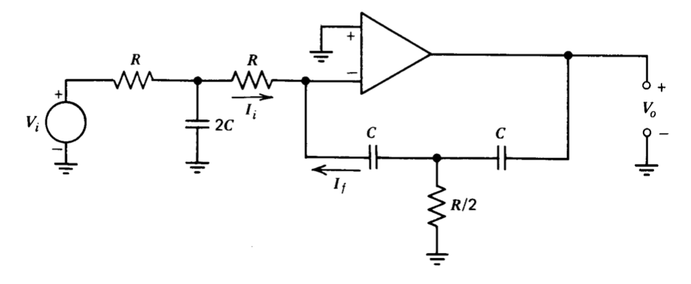
We have seen that either inverting or noninverting integration can be accomplished with an operational amplifier. Figure 11.12 shows a connection that provides a second-order integration with a single operational amplifier. The circuit is analyzed by the virtual-ground method. Assuming that the inverting input of the amplifier is at ground potential
\[I_i (s) = \dfrac{V_i (s)}{2R(RCs + 1)} \label{eq11.4.8} \]
and
\[I_f (s) = \dfrac{RC^2 s^2 V_o (s)}{2(RCs + 1)} \label{eq11.4.9} \]
The negligible input current of the amplifier forces \(I_f = -I_i\). Combining and Equations \(\ref{eq11.4.8}\) and \(\ref{eq11.4.9}\) via this constraint shows that
\[\dfrac{V_o (s)}{V_i (s)} = -\dfrac{1}{(RCs)^2} \nonumber \]
Current Sources
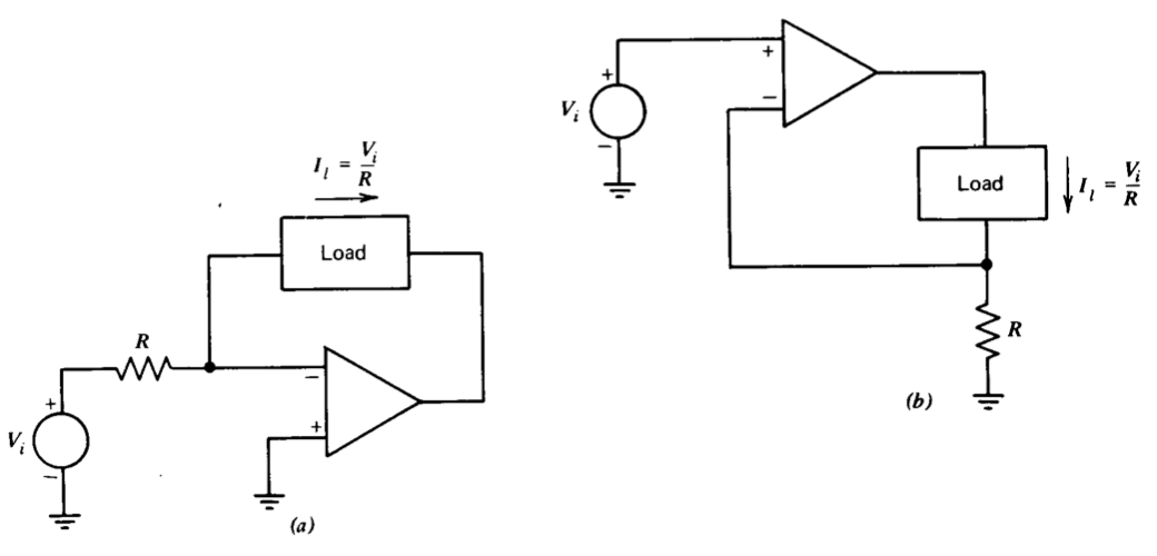
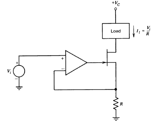
The operational amplifier can be used as a current source in a number of different ways. Figure 11.13 shows two simple configurations. In part \(a\) of this figure, the load serves as the feedback impedance of an inverting-connected operational amplifier. The virtual-ground method shows that the current through the load must be equal to the current through resistor \(R\). In part \(b\), the operational amplifier forces the voltage across \(R\) to be equal to the input voltage. Since the current required at the inverting input terminal of the amplifier is negligible, the load current is equal to the current through resistor \(R\).
Both of the current-source connections described above require that the load be floating. The configuration shown in Figure 11.14 relaxes this requirement. Here the operational amplifier constrains the source current of a field-effect transistor. Provided that operating levels are such that the FET gate is reverse biased, the source and drain currents of this device are identical. Thus the operational amplifier controls the load current indirectly.
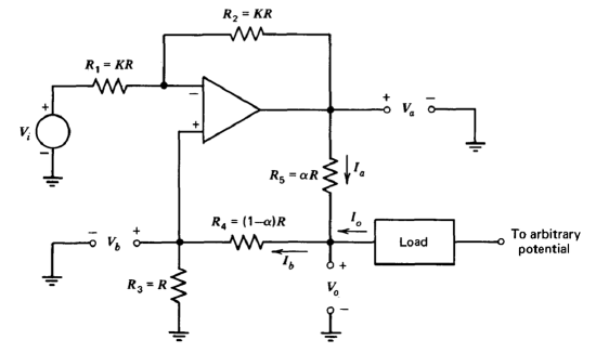
The relative operating levels of the circuit shown in Figure 11.14 must be constrained to keep the FET in its forward operating region with its gate reverse biased for satisfactory performance. The Howland current source shown in Figure 11.15 allows further freedom in the choice of operating levels.
The analysis of this circuit is simplified by noting that the operational amplifier relates \(V_a\) to \(V_i\) and \(V_b\) as
\[V_a = -V_i + 2V_b \label{eq11.4.11} \]
The circuit topology implies the relationships
\[I_o = I_b - I_a \nonumber \]
\[I_a = \dfrac{V_a - V_o}{\alpha R} \nonumber \]
\[I_b = \dfrac{V_o - V_b}{(1 - \alpha )R} \nonumber \]
and
\[V_b = \dfrac{V_o}{2 - \alpha} \label{eq11.4.15} \]
The transfer relationships of interest for this circuit are the input voltage to short-circuit output current transconductance \(I_o/ V_i\) and the output conductance of the circuit \(I_o/V_o\). Solving Equations \(\ref{eq11.4.11}\) through \(\ref{eq11.4.15}\) for these conductances shows that
\[\dfrac{I_o}{V_i}|_{V_o = 0} = \dfrac{1}{\alpha R} \nonumber \]
and
\[\dfrac{I_o}{V_o}|_{V_i = 0} = 0 \nonumber \]
Since the output current is independent of output voltage, we can model the circuit as a current source with a magnitude dependent on input voltage. While the output resistance of this current source is independent of the quantity \(\alpha\), this parameter does affect scale factor. Smaller values of \(\alpha R\) also allow a greater maximum output current for a given output voltage saturation level from the operational amplifier. There is a tradeoff involved in the selection of \(\alpha\), however, since smaller values for this parameter result in higher error currents for a given offset voltage referred to the input of the amplifier (see Problem P11.11).
There is further freedom in the selection of relative resistor ratios, since an extension of the above analysis shows that the output resistance is infinite provided \(R_2/R_1 =(R_4+R_5)/R_3\).
It is interesting to note that the success of this current source actually depends on positive feedback. Consider a voltage \(V_o\) applied to the output terminal of the circuit. The current that flows through resistor \(R_4\) is exactly balanced by current supplied from the output of the operational amplifier via resistor \(R_5\). The voltage at the output of the operational amplifier is the same polarity as \(V_o\) and has a larger magnitude than this variable.
We should further note that the resistor \(R_3\) does not have to be connected to ground, but can also function as an input terminal. In this configuration the output current is proportional to the difference between the voltages applied to the two inputs.
Circuits which Provide a Controlled Driving-Point Impedance
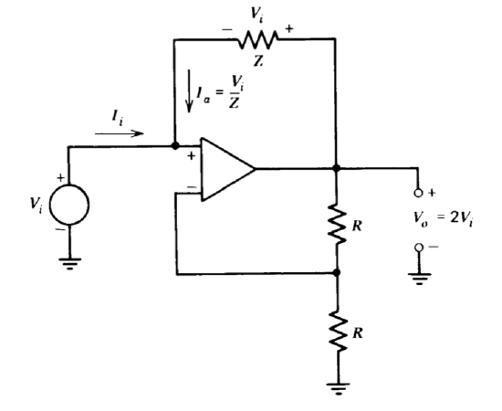
We have seen examples of circuits designed to produce very high or very low input or output impedances. It is also possible to use operational amplifiers to produce precisely controlled output or driving-point impedances. Consider the circuit shown in Figure 11.16. The operational amplifier is configured to provide a noninverting gain of two. As a result of this gain, the impedance connected between the amplifier output and its noninverting input has a voltage \(V_i\) across it with a polarity as shown in Figure 11.16. Since there is negligible current required at the inverting input of the amplifier, the input current required from the source is
\[I_i = -I_a = -\dfrac{V_i}{Z} \label{eq11.4.18} \]
Solving Equation \(\ref{eq11.4.18}\) for the input impedance of the circuit yields
\[\dfrac{V_i}{I_i} = -Z \label{eq11.4.19} \]
Equation \(\ref{eq11.4.19}\) shows that this circuit has sufficient positive feedback to produce negative input impedances.
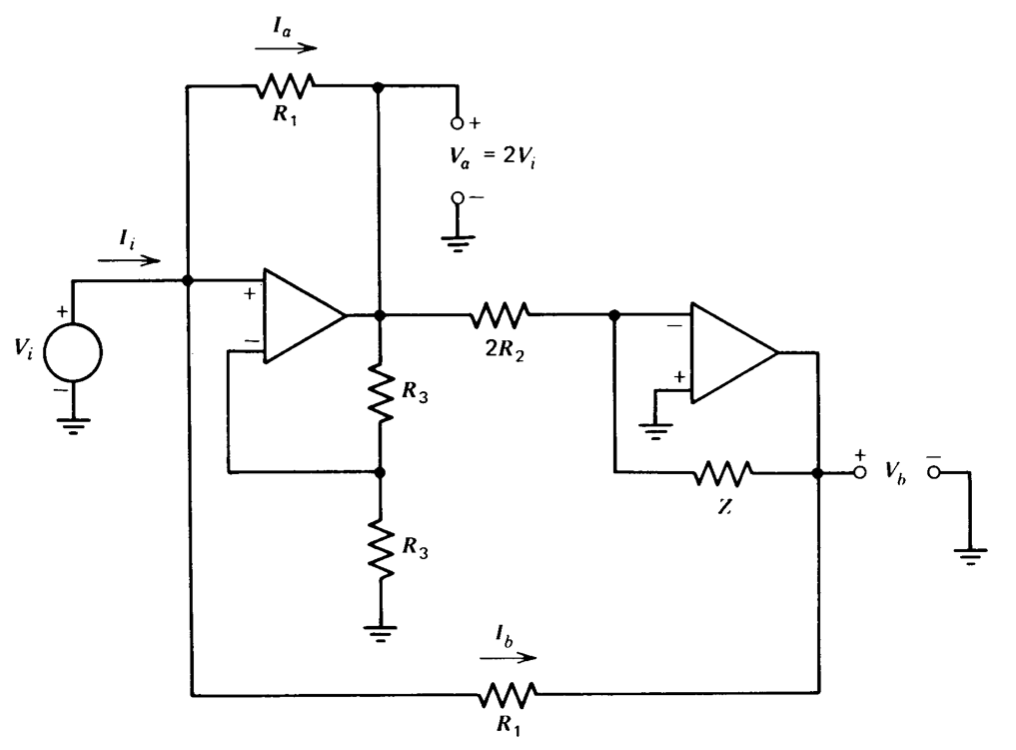
The gyrator shown in Figure 11.17 is another example of a circuit that provides a controlled driving-point impedance. The circuit relationships include
\[I_i = I_a + I_b \label{eq11.4.20} \]
\[I_a = \dfrac{V_i - V_a}{R_1} = \dfrac{-V_i}{R_1} \nonumber \]
\[I_b = \dfrac{V_i - V_b}{R_1} \nonumber \]
\[V_b = -\dfrac{V_i Z}{R_2} \label{eq11.4.23} \]
Combining Equations \(\ref{eq11.4.20}\) through \(\ref{eq11.4.23}\) and solving for the driving-point impedance shows that
\[\dfrac{V_i}{I_i} = \dfrac{R_1 R_2}{Z} \nonumber \]
We see that the gyrator provides a driving-point impedance that is reciprocally related to another circuit impedance. Applications include the synthesis of elements that function as inductors using only capacitors, resistors, and operational amplifiers. For example, if we choose impedance \(Z\) to be a \(1-\mu F\) capacitor and \(R_1 = R_2 = 1\ k\Omega\), the driving-point impedance of the circuit shown in Figure 11.17 is \(s\), equivalent to that of a 1-henry inductor.