
12.5: FURTHER EXAMPLES
- Page ID
- 75435

It was mentioned in the introduction to Chapter 11 that the objective of the application portion of this book was to illustrate concepts for design rather than to provide specific, detailed examples in the usually futile hope that the reader could apply them directly to his own problems. Successful design almost always involves combining bits and pieces, a concept here, a topology there, to ultimately arrive at the optimum solution. In this section we will see how some of the ideas introduced earlier are combined into relatively more sophisticated configurations. The three examples that are presented are all "real world" in that they reflect actual requirements that the author has encountered recently in his own work.
Frequency-Independent Phase Shifter
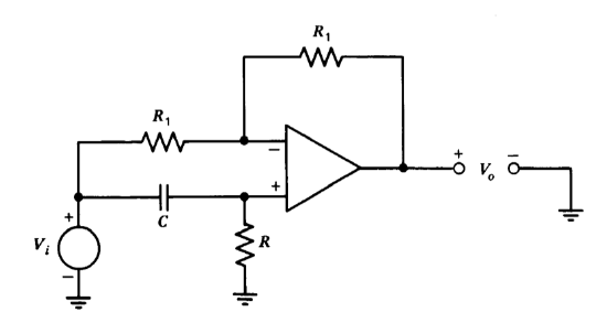
There are a number of operational-amplifier connections, such as the approximation to a time delay described in the previous section, that have a transfer-function magnitude independent of frequency combined with specified phase characteristics. The phase shifter shown in Figure 12.30 is another example of this type of circuit. We recognize this circuit as a differential-amplifier connection, and thus realize that its transfer function is
\[\dfrac{V_o (s)}{V_i (s)} = \left (\dfrac{2RCs }{RCs + 1} - 1 \right ) = \dfrac{RCs - 1}{RCs + 1} \nonumber \]
This transfer function (which is the negative of a first-order Pade approxi mate to a time delay of \(2RC\) seconds) produces a phase shift that varies from \(-180^{\circ}\) at low frequencies to \(0^{\circ}\) at high frequencies. If a potentiometer or a field-effect transistor is used for \(R\), the phase shift can be manually or electronically varied.
One technique for converting resolver(A resolver is basically a transformer with a primary-to-secondary coupling that can be varied by mechanically changing the relative alignment of these windings. This device is used as a rugged and highly accurate mechanical-angle transducer.) signals to digital form requires that a fixed \(90^{\circ}\) phase shift be applied to a sinusoidal signal with no change in its amplitude. The frequency of the signal to be phase shifted may change by a few percent. Unfortunately, there are no finite-polynomial linear transfer functions that combine frequency-independent magnitude characteristics with a constant 900 phase shift. While approximating functions do exist over restricted frequency ranges, the arc-minute phase-shift constancy required in this application precluded the use of such functions. We note that since a very specific class of input signals (single-frequency sinusoids) is to be applied to the phase shifter, linearity may not be a necessary constraint. Nonlinear circuits, in spite of our inability to analyze them systematically, often have very interesting properties.
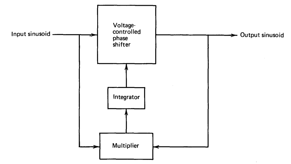
Consider the configuration shown diagrammatically in Figure 12.31 as a possible solution to our problem. In this circuit, an all-pass phase shifter with a voltage-variable amount of phase shift is the central element. The circuit shown in Figure 12.30 with a field-effect transistor used for the resistor \(R\) can perform this function. The multiplier is used as a phase detector. If the magnitude of the phase shift between the input and output signals is less than \(90^{\circ}\), the average value of the multiplier output will be positive, while if this magnitude is between \(90^{\circ}\) and \(180^{\circ}\), the average multiplier out put signal will be negative. The integrator, which provides the control
voltage for the FET in the phase shifter, filters the second harmonic that results from the multiplication and supplies the loop gain necessary to keep the average value of the multiplier output at zero, thus forcing a 900 phase shift between input and output signals. Although the circuit described above can result in moderate accuracy, a detailed investigation indicated that meeting the required specifications probably was not practical with this topology.
It is worth noting that while the basic approach described above was not used in this case, it is a valuable technique that has a number of interesting and useful variations. For example, the phase shift of a second-order high- or low-pass active filter is \(\pm 90^{\circ}\) when excited at its corner frequency. Tracking filters can be realized by replacing the fixed resistors in an active filter with voltage-controlled resistors and using a phase comparison to locate the corner frequency of the filter at its excitation frequency.
In some applications, other types of phase detectors are used. One possibility involves high-gain limiters that produce square waves with zero crossing synchronized to those of the sine waves of interest. The duty cycle of an exclusive OR gate operating on the square waves indicates the relative phase of the original signals.
The previous circuit combined an all-pass network that provides a transfer-function magnitude that is independent of frequency with feedback which forces \(90^{\circ}\) of phase shift at the operating frequency. An alternative approach is to combine a network that provides \(90^{\circ}\) of phase shift at all frequencies (an integrator) with feedback that forces its gain magnitude to be one at the operating frequency.
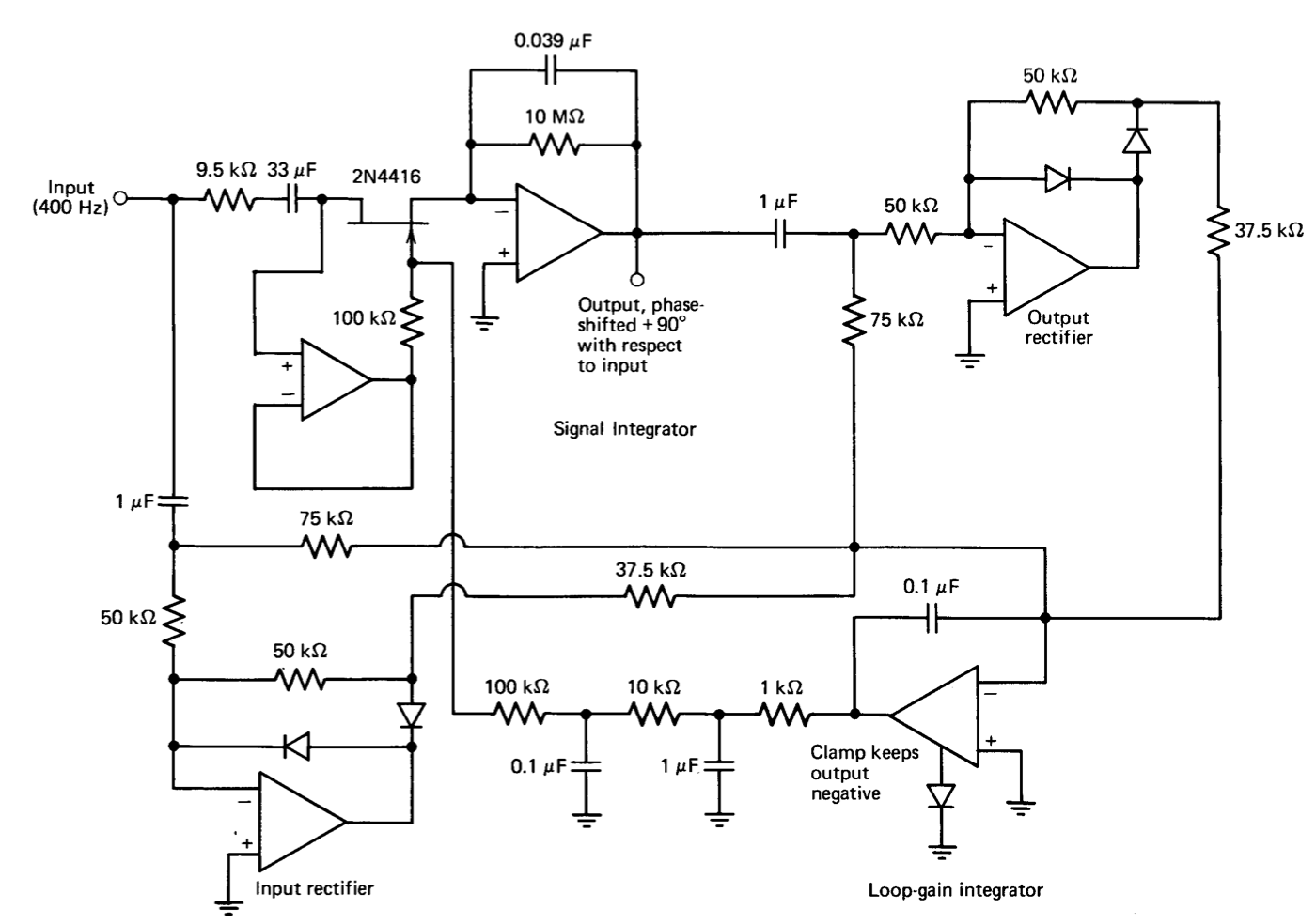
The circuit that evolved to implement the above concept is shown in only slightly simplified form in Figure 12.32. The signal integrator provides the required 90' of phase shift. Its scale factor is adjusted by means of the field-effect transistor so that a gain magnitude of one is provided at frequencies close to the nominal operating value of 400 Hz. Half of the drain-to-source voltage of the field-effect transistor is applied to its gate to linearize the drain-to-source resistance as described in Section 12.1.4. The unity-gain buffer amplifier prevents current flowing through the FET-gate network from being integrated. The capacitor in series with the signal-integrator input resistor and the resistor shunting the integrating capacitor are required to keep this integrator from saturating as a consequence of input voltage offset and bias current. While they change the ideal phase shift by a total of approximately eight arc minutes, this value is trimmed out along with other phase-shift errors with a network (not shown) following the integrator.
The two full-wave precision-rectifier connections combine with the loop-gain integrator to provide an average current into the capacitor of this integrator that is proportional to the difference between the magnitudes of the input and output signals. If, for example, the output-signal magnitude exceeds the input-signal magnitude, the voltage out of the loop-gain integrator is driven negative. This action increases the incremental resistance of the FET, thus decreasing the signal-integrator scale factor and lowering the magnitude of the output signal. The inputs to the precision rectifiers are a-c coupled so that d-c components of these signals do not influence the rectifier output signals. A two-pole low-pass filter follows the loop-gain integrator to further filter harmonics that would degrade signal-integrator performance.
The maximum positive output level of the loop-gain integrator is clamped via an internal node to a maximum output level of zero volts in order to eliminate a latch-up mode. If this voltage became positive, the FET would conduct gate current, and this current could cause the signal-integrator output to saturate. As a result, the a-c component of the signal-integrator output would be eliminated, and the loop, in an attempt to restore equilibrium, would drive the output of the loop-gain integrator further positive. The diode clamp prevents initiation of this unfortunate chain of events.
The circuit shown in Figure 12.32 has been built and tested at operating frequencies between 395 and 405 Hz over the temperature range of \(0^{\circ}\) to \(50^{\circ}\) Centigrade. (The feedback also eliminates the effects of signal-integrator component-value changes with temperature.) The input- and output-signal amplitudes remain equal within I mV peak-to-peak at any input-signal level up to 20 volts peak-to-peak. The phase shift of the circuit with a 20 volt peak-to-peak input remains constant within one arc minute. While the actual phase shift is not precisely \(90^{\circ}\), the constant component of the phase error can be trimmed out as described earlier.
Sine-Wave Shaper
We have discussed certain aspects of a function-generator circuit that combines an integrator and a Schmitt trigger to produce square and triangle waves in Sections 6.3.3 and 12.2.1. Commercial versions of this circuit usually also provide a sine-wave output that is synthesized by the seemingly improbable .method of shaping the triangle wave with a piecewise-linear network. This technique is practical because of the ease of generating variable-frequency triangular waves, and because the use of relatively few segments in the shaping network gives surprisingly good sine-wave fidelity.
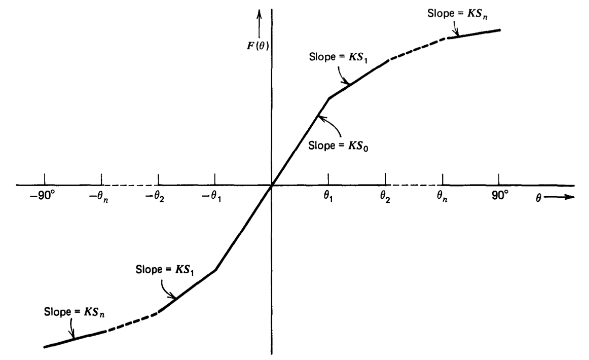
Part of the design problem is to determine how the characteristics of the shaping network should be chosen to best approximate a sine wave. The parameters that define the network are shown in Figure 12.33. A total of n break points are located over the input-variable range of \(0^{\circ}\) to \(90^{\circ}\). The
slope of the input-output transfer relationship is \(KS_m\) between \(\theta = \theta_m\) and \(\theta = \theta_{m+1}\). The multiplying constant \(K\) reflects the fact that only relative slopes are important, since a multiplicative change in all slopes changes only the magnitude of the input-output transfer characteristics. The symmetry of the transfer characteristics about the origin insures that the output signal will have no d-c component and will contain no even harmonics when a zero-average-value triangular signal is used as the input.
The network specification involves the choice of \(n\) values of \(\theta\) (the breakpoint locations) and \(n + 1\) relative slopes. It can be shown that if the \(\theta\)'s are selected such that
\[\theta_m = \dfrac{m 180^{\circ}}{2n + 1} \ \ \ 0 \le m \le n \label{eq12.5.2} \]
and slopes selected as
\[S_m = \sin \theta_{m + 1} - \sin \theta_m \ \ \ 0 \le m < n \label{eq12.5.3} \]
\[S_m = 0 \ \ \ m = n \label{eq12.5.4} \]
put distortion resulting from imprecise break-point locations and slope values is comparable to the distortion associated with the piecewise-linear approximation unless expensive components are used to establish these parameters. Furthermore, an inexpensive integrated-circuit five-diode array is available. This matched-diode array can be used for the four break points, with the fifth diode providing temperature compensation as described in material to follow. Equations \(\ref{eq12.5.2}\), \(\ref{eq12.5.3}\) and \(\ref{eq12.5.4}\) evaluated for \(n = 4\) suggest break points located at input-variable values of \(20^{\circ}\), \(40^{\circ}\), \(60^{\circ}\), and \(80^{\circ}\), with relative segment slopes (normalized to a minimum nonzero slope of one) of 2.879, 2.532, 1.879, 1, and 0, respectively.
With the transfer characteristics of the shaping network determined, it is necessary to design the circuit that synthesizes the required function. The discussion of Section 11.5.3 mentioned the use of superdiode connections to improve the sharpness of break points compared to that which can be achieved with diodes alone. This technique was not used for the sine shaper, since the rounding associated with the normal diode forward characteristics actually improves the quality of the fit to the sine curve.
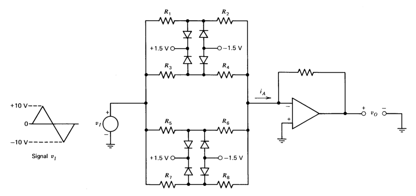
The compressive type nonlinearities described in Section 11.5.3 were realized using diodes to increase the feedback around an operational amplifier, thus reducing its incremental closed-loop gain when a breakpoint level was exceeded. An alternative is to use diodes to decrease the drive signal applied to the amplifier to lower incremental gain. This approach simplifies temperature compensation. The topology used is shown in Figure 12.34.
The input-signal level of 20 volts peak-to-peak corresponds to the input variable range of \(\pm 90^{\circ}\) shown in Figure 12.33. Thus the break-point locations of \(\pm 20^{\circ}\), \(\pm 40^{\circ}\), \(\pm 60^{\circ}\), and \(\pm 80^{\circ}\) correspond to input-voltage levels of \(\pm 2.22\) volts, \(\pm 4.44\) volts, \(\pm 6.67\) volts, and \(\pm 8.89\) volts, respectively. Resistor values are determined as follows. It is initially assumed that the diodes are ideal, in that they have a threshold voltage of zero volts, zero resistance in the forward direction, and zero conductance in the reverse direction. Assume that the \(R_1-R_2\) path is to provide the break points at input voltages of \(\pm 8.89\) volts. Since the inverting input of the operational amplifier is at ground potential, the resistor ratio necessary to make the voltage at the midpoint of these two resistors \(\pm 1.5\) volts with \(\pm 8.89\) volts at the input is
\[\dfrac{R_2}{R_1 + R_2} = \dfrac{1.5}{8.89} = 0.1687 \label{eq12.5.5} \]
The ratios of resistor pairs \(R_3-R_4\), \(R_5-R_6\), and \(R_7-R_8\) are chosen in a similar way to locate the remaining break points.
The relative conductances of the resistive paths between the triangular- wave signal source and the inverting input of the operational amplifier are constrained by the relative slopes of the desired transfer characteristics as follows. The closed-loop incremental gain of the connection is proportional to the incremental transfer conductance from the signal source to the current \(i_A\) defined in Figure 12.34. With the ratio of the two resistors in each path chosen in accordance with relationships like Equation \(\ref{eq12.5.5}\), the incre mental transfer conductance is zero (for ideal diodes) when the input- signal magnitude exceeds 8.89 volts, increases to \(1/(R_1 + R_2)\) for input-signal magnitudes between 6.67 and 8.89 volts,, increases further to \([1/(R_1 + R_2)] + [1/(R_3 + R_4)]\) for input-signal magnitudes between 4.44 and 6.67 volts, etc. If we define \(1/(R_1 + R_2) = G\), realizing the correct relative slope for input-signal magnitudes between 4.44 and 6.67 volts requires
\[\dfrac{1}{R_1 + R_2} + \dfrac{1}{R_3 + R_4} = 1.879 G \label{eq12.5.6} \]
The satisfaction of Equation \(\ref{eq12.5.6}\) makes the slope in this input signal range 1.879 times as large as the slope for input signals between 6.67 and 8.89 volts. Corresponding relationships couple other resistor-pair values to the \(R_1-R_2\) pair.
The sets of equations that parallel Equations \(\ref{eq12.5.5}\) and \(\ref{eq12.5.6}\), together with the selection of any one resistor value, determine reistors \(R_1\) through \(R_8\). The general resistance level set by choosing the one free resistor value is selected based on loading considerations and to insure that stray capacitance does not deteriorate dynamic performance.
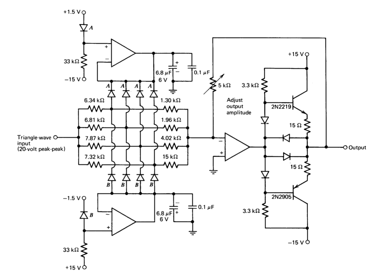
The circuit used for the sine shaper (Figure 12.35) uses the standard 1%-tolerance resistor values that best approximate calculated values. The five diodes labeled \(A\) and those labeled \(B\) are from two CA3039 integrated- circuit diode arrays. One member of each array modifies the bias voltages to account for the diode threshold voltages and to provide temperature compensation. The compensating diodes are operated at a current level of approximately half the maximum operating current level of the shaping diodes. While this type of compensation clearly has no effect on the conductance characteristics of the shaping diodes, the exponential diode characteristics actually improve the performance of the circuit as described earlier.
Since this circuit is intended to operate to 1 MHz (a high-speed integrated- circuit operational amplifier with a discrete-component buffer to increase output-current capacity is used), capacitors are necessary at the output of the reference-voltage amplifiers to lower their output impedance at the switching frequency of the diodes. The \(1.5-V\) levels are derived from the voltages that establish triangle-wave amplitude so that any changes in this amplitude cause corresponding break-point location changes.
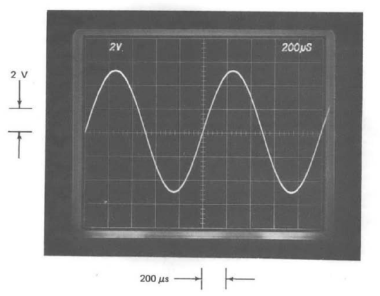
The circuit produces approximate sine waves with the amplitude of any individual harmonic in the output signal at least 40 dB (a voltage ratio of 100:1) below the fundamental. This performance is obtained with no trimming. If adjustments are made to null the offset of the operational amplifier, and empirical adjustments (guided by a spectrum analyzer) are used to counteract component-value errors and to compensate for finite diode forward resistance, the amplitude of individual output-signal harmonics can be reduced to 55 dB below the fundamental at low frequencies. Performance deteriorates somewhat at frequencies above approximately 10 kHz because of reduced signal-amplifier open-loop gain. A 1-kHz output signal from the circuit is shown in Figure 12.36.
Nonlinear Three-Port Network
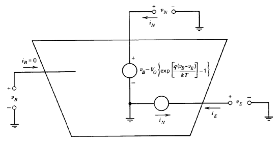
The realization of a device analog that may be of value in teaching the dynamic behavior of bipolar transistors requires a three-port network defined by Figure 12.37. The synthesis of this network is initiated by first designing a circuit that provides the relationship
\[v_N = v_B - V_0 \left \{\exp \left [\dfrac{q(v_B - v_E)}{kT} \right ] - 1 \right \}\label{eq12.5.7} \]
The parameter \(V_O\), as we might expect, is related to the quantity \(I_S\) for the transistor being simulated, and consequently a corresponding temperature dependence is desirable.
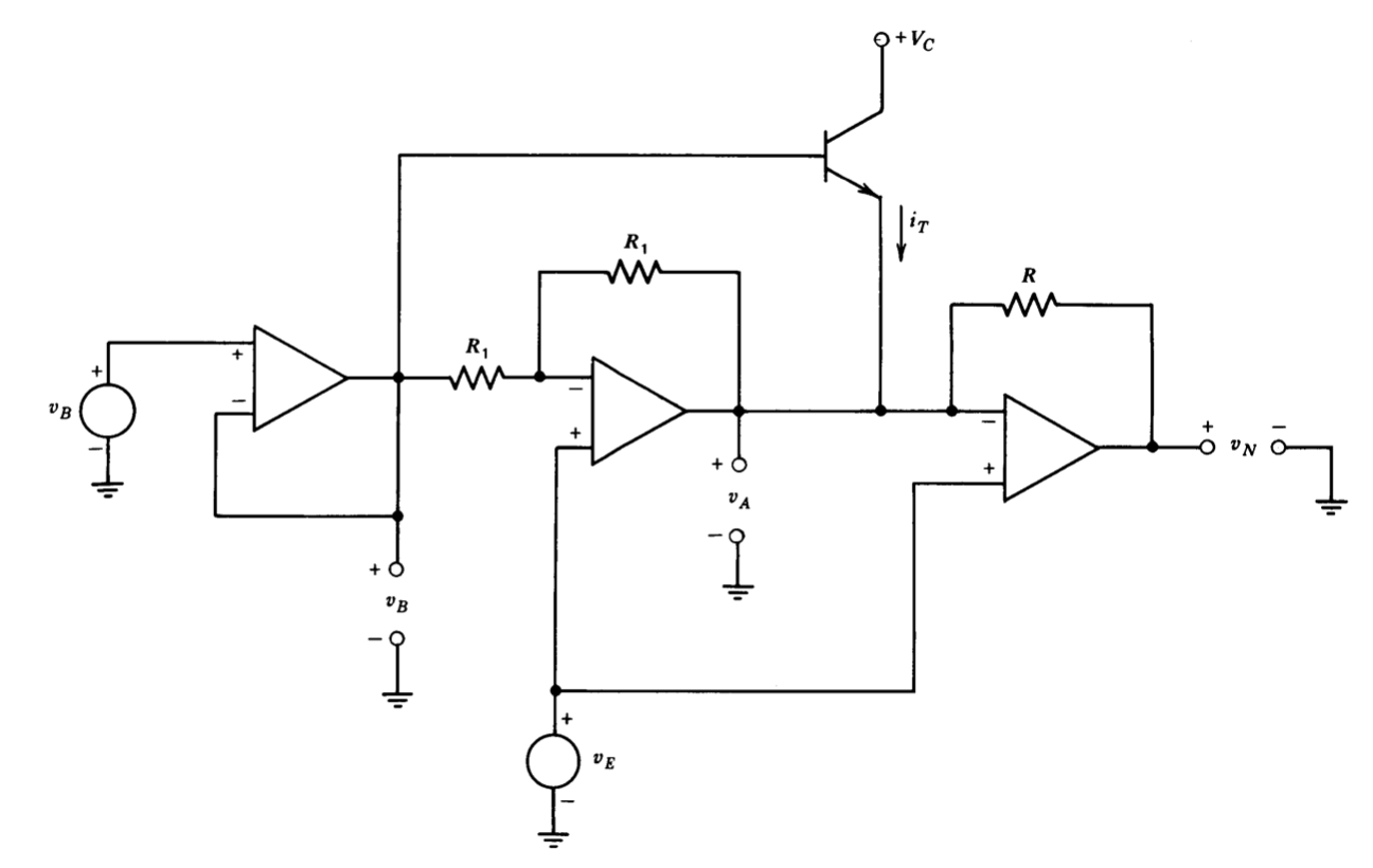
There are a number of ways to simulate Equation \(\ref{eq12.5.7}\). One topology that is adaptable to further requirements is shown in Figure 12.38. Since an eventual constraint is that the current at the \(v_B\) input be zero, a buffer amplifier is used at this terminal. The second amplifier is differentially connected with an output voltage.
\[v_A = 2v_E - v_B\label{eq12.5.8} \]
The third amplifier is also connected as a differential amplifier, so that
\[v_N = v_E - (i_T + i_A) R \label{eq12.5.9} \]
Since feedback keeps the inverting input terminal of the third amplifier at potential \(v_E\),
\[i_A = \dfrac{v_A -v_E}{R} = \dfrac{v_E - v_B}{R} \label{eq12.5.10} \]
If we assume the usual transistor characteristics,
\[i_T \simeq I_S \left \{ \exp \left [\dfrac{q(v_B - v_E)}{kT} \right ] - 1 \right \}\label{eq12.5.11} \]
Substituting Equations \(\ref{eq12.5.10}\) and \(\ref{eq12.5.11}\) into Equation \(\ref{eq12.5.9}\) yields the form required by Equation \(\ref{eq12.5.8}\):
\[v_N = v_B - RI_S \left \{ \exp \left [\dfrac{q(v_B - v_E)}{kT} \right ] - 1 \right \} \nonumber \]
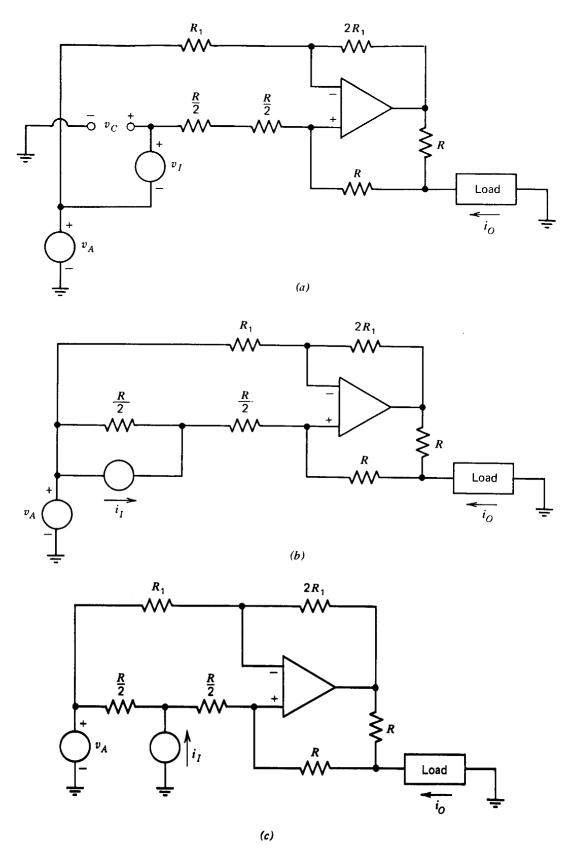
In order to complete the synthesis, it is necessary to sample the current flowing at terminal \(N\) and make the current flowing at terminal \(E\) the negative of this current. A modification of the Howland current source (see Section 11.4.3) can be used. The basic circuit with differential inputs is shown in Figure 12.39\(a\). (The reason for the seemingly strange input-voltage connection and the split resistor will become apparent momentarily.) The current \(i_O\) for these parameter values is
\[i_O = \dfrac{2(v_A - v_C)}{R} = \dfrac{2(v_A - v_A - v_I}{R} = \dfrac{-2v_I}{R}\label{eq12.5.13} \]
In Figure 12.39\(b\), the voltage source \(v_I\) and half of the split resistor are replaced with a Norton-equivalent circuit. For equivalence, it is necessary to make \(i_I = 2v_I/R\). Expressing Equation \(\ref{eq12.5.13}\) in terms of \(i_I\) shows
\[i_O = -i_I \nonumber \]
The topology of Figure 12.39\(b\) shows that the \(i_T\) current source can be returned to ground rather than to voltage source \(v_A\). This modification is shown in Figure 12.39\(c\), the current-controlled current source necessary in our present application. Note that the output is independent of \(v_A\), the common-mode input voltage applied to the current source.
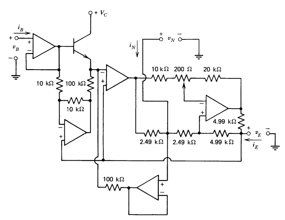
The circuits of Figs. 12.38 and 12.39\(c\) are combined to form the three-port network as shown in Figure 12.40. In this circuit, the feedback for the voltage \(v_N\) is taken from the output side of the current-sampling resistor so that voltage drops in this resistor do not influence \(v_N\). It is necessary to buffer the \(100-k\Omega\) feedback resistor with a unity-gain follower to insure that current through this resistor does not flow through the current-sampling resistor and thus alter \(i_E\).
The trim potentiometer allows precise matching of resistor ratios to make current \(i_E\) independent of common-mode voltage levels at various points in the current source and thus dependent only on \(i_N\). In this application, it was not necessary to have exactly unity gain between \(i_N\) and \(- i_E\), so no trim is included for this ratio. The general magnitude of the resistors in the current source is chosen for compatibility with required current levels and amplifier characteristics and is not important for purposes of this discussion.
Exercise \(\PageIndex{1}\)
Consider a Wien-Bridge oscillator as shown in Figure 12.1. Show that if the output signal is of the general form \(v_O = E \sin [(t/RC) + \theta]\) where \(\theta\) is a constant, the signals applied to the two inputs of the operational amplifier are virtually identical, a necessary condition for satisfactory performance. Note that if the inverting and noninverting inputs are interchanged and it is assumed that the output has the form indicated above, the signals at the two inputs will also be identical. However, this modified topology will not function as an oscillator. Explain.
Exercise \(\PageIndex{2}\)
A Wien-Bridge oscillator is constructed using the basic topology shown in Figure 12.1. Because of component tolerances, the time constants of the series and parallel arms of the frequency-dependent feedback network differ by 5%. How must component values in the frequency-independent feedback path be related to guarantee oscillation?
Exercise \(\PageIndex{3}\)
Use a describing-function approach to analyze the circuit shown in Figure 12.3, assuming that the operational amplifier is ideal and that the diodes have zero conductance until a forward voltage of 0.6 volt is reached and zero resistance in the forward-conducting state. In particular, determine the magnitude of the signal applied to the noninverting input of the amplifier and the third-harmonic distortion present at the amplifier output.
Exercise \(\PageIndex{4}\)
A sinusoidal oscillator is constructed by connecting the output of a double integrator (see Figure 11.12) to its input. Show that amplitude can be controlled by varying the magnitude of the (\(R/2\))-valued resistor shown in this figure. Design a complete circuit that can produce a \(20-V\) peak-to-peak output signal at 1 kHz. Use a FET with parameters given in Section 12.1.4 for the control element. Analyze your amplitude-control loop to show that it has acceptable stability and a crossover frequency compatible with the 1-kHz frequency of oscillation. If you have confidence in your design, build it. The 2N4416 field-effect transistor is reasonably well characterized by the parameters referred to above.
Exercise \(\PageIndex{5}\)
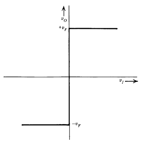
The discussions of Sections 12.2.2 and 12.2.3 suggest operating electronic switches connected to symmetrical, variable voltages from the output of a Schmitt trigger for two different applications. An alternative to the use of switches is to use a circuit that has the transfer characteristic shown in Figure 12.41 for the necessary shaping function. (In this diagram, the voltage \(v_F\) is a positive variable.) Design a circuit that uses operational amplifiers to synthesize this transfer characteristic. Your output levels should be insensitive to temperature variations.
Exercise \(\PageIndex{6}\)
A magnetic-suspension system was described in Section 6.2.3. Develop an electronic analog simulation of this system that permits determination of the transients that result from disturbing forces applied to the ball. Assume that, in addition to operational amplifiers and appropriate passive components, multipliers with a scale factor \(v_O = v_Xv_Y/10\) volts are available. A way to perform the division required in this simulation using a multiplier and an operational amplifier is outlined in Section 6.2.2.
You may leave the various element values in the simulation defined in terms of system parameters, without developing final amplitude-scaled values.
Exercise \(\PageIndex{7}\)
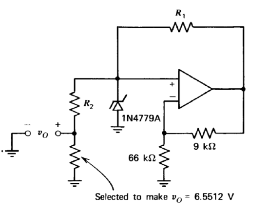
A circuit intended for use as a precision voltage reference for an analog-to-digital converter is shown in Figure 12.42. The circuit uses a fraction of the Zener-diode voltage as its output. While this method involving resistive attenuation results in relatively high output resistance compared with using the voltage at the output of the amplifier as the reference, the output voltage becomes essentially independent of operational-amplifier offset voltage.
The specified breakdown voltage of the 1N4779A is 8.5 volts \(\pm 5\)%. The indicated resistor is selected during testing to obtain the required output voltage independent of the actual value of the Zener-diode voltage.
The breakdowh voltage range and the temperature coefficient of the device are guaranteed at an operating current of \(0.500\ mA\). By proper choice of \(R_1\) and \(R_2\), it is possible to make the current through the Zener diode independent of the actual Zener voltage after the single indicated selection has been completed. Such a choice is advantageous since it simplifies circuit calibration as opposed to methods that require two or more interdependent adjustments to set output voltage and Zener-diode operating current. Find values for \(R_1\) and \(R_2\) that result in this simplification. (Please excuse the somewhat unwieldy numbers involved in this problem, but it is drawn directly from an existing application.)
Exercise \(\PageIndex{8}\)
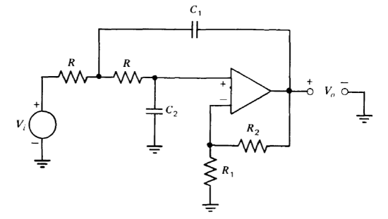
A Sallen and Key low-pass circuit with an amplifier closed-loop voltage gain greater than unity is shown in Figure 12.43. Determine the transfer function \(V_o(s)/V_i(s)\) for this circuit. Compare the sensitivity of this circuit to component variations with that of the unity-gain version.
Exercise \(\PageIndex{9}\)
One way to analyze the Sallen and Key circuit shown in Figure 12.43 is to recognize the configuration as a positive-feedback circuit. If the loop is broken at the noninverting input to the operational amplifier, analysis techniques based on loop-transmission properties can be used.
(a) Indicate the loop-transmission singularity pattern that results when the loop is broken at the point mentioned above. It is not necessary to determine singularity locations exactly in terms of element values.
(b) Show how the closed-loop poles of the system move as a function of the closed-loop gain of the operational amplifier by using root-locus methods that have been appropriately modified for positive feedback systems.
Exercise \(\PageIndex{10}\)
Design a sixth-order Butterworth filter with a 1 kHz corner frequency by cascading three unity-gain Sallen and Key circuits.
Exercise \(\PageIndex{11}\)
The fifth-order Pad6 approximate to a one-second time delay is
\[P_5 (s) = \dfrac{1 - 0.5s + 0.111s^2 - 1.39 \times 10^{-2} s^3 + 9.92 \times 10^{-4} s^4 - 3.31 \times 10^{-5} s^5}{1 + 0.5s + 0.111s^2 - 1.39 \times 10^{-2} s^3 + 9.92 \times 10^{-4} s^4 + 3.31 \times 10^{-5} s^5}\nonumber \]
Design an active filter that synthesizes this transfer function.
Exercise \(\PageIndex{12}\)
Develop a linearized block-diagram for the system shown in Figure 12.32, assuming that the FET is characterized by the parameters given in Section 12.1.4. Show that the loop crossover frequency is low compared to 400 Hz for any input-voltage level up to 20 volts peak-to-peak. Estimate the time required for the system to restore equilibrium following an incremental perturbation (initiated, for example, by a change in input frequency) when the input-signal amplitude is 100 mV peak-to-peak. Note that the system is not significantly disturbed by a change in input amplitude when operating under equilibrium conditions, and that therefore this relatively long settling time does not deteriorate performance.