
13.3: COMPENSATION BY CHANGING THE AMPLIFIER TRANSFER FUNCTION
- Page ID
- 58483

If the open-loop transfer function of an operational amplifier is fixed, this constraint, combined with the requirement of achieving a specified ideal closed-loop transfer function, severely restricts the types of modifications that can be made to the loop transmission of connections using the amplifier. Significantly greater flexibility is generally possible if the open-loop transfer function of the amplifier can be modified. There are a number of available integrated-circuit operational amplifiers that allow this type of control. Conversely, very few discrete-component designs are intended to be compensated by the user. The difference may be historical in origin, in that early integrated-circuit amplifiers used shunt impedances at various nodes for compensation (see Section 8.2.2) and the large capacitors required could not be included on the chip. Internal compensation became practical as the two-stage design using minor-loop feedback for compensation evolved, since much smaller capacitors are used to compensate these amplifiers. Fortunately, the integrated-circuit manufacturers choose to continue to design some externally compensated amplifiers after the technology necessary for internal compensation evolved.
In this section, some of the useful open-loop amplifier transfer functions that can be obtained by proper external compensation are described, and a number of different possibilities are analytically and experimentally evalu ated for one particular integrated-circuit amplifier.
General Considerations
An evident question concerning externally compensated amplifiers is why they should be used given that internally compensated units are available. The answer hinges on the wide spectrum of applications of the operational amplifier. Since this circuit is intended for use in a multitude of feedback applications, it is necessary to choose its open-loop transfer function to insure stability in a variety of connections when this quantity is fixed.
The compromise most frequently used is to make the open-loop transfer function of the amplifier dominated by one pole. The location of this pole is chosen such that the amplifier unity-gain frequency occurs below frequencies where other singularities in the amplifier transfer function contribute excessive phase shift.
This type of compensation guarantees stability if direct, frequency-independent feedback is applied around the amplifier. However, it is overly conservative if considerable resistive attenuation is provided in the feedback path. In these cases, the crossover frequency of the amplifier with feedback drops, and the bandwidth of the resultant circuit is low. Conversely, if the feedback network or loading adds one or more intermediate-frequency poles to the loop transmission, or if the feedback path provides voltage gain, stability suffers.
However, if compensation can be intelligently selected as a function of the specific application, the ultimate performance possible from a given amplifier can be achieved in all applications. Furthermore, the compensation terminals make available additional internal circuit nodes, and at times it is possible to exploit this availability in ways that even the manufacturer has not considered. The creative designer working with linear integrated circuits soon learns to give up such degrees of freedom only grudgingly.
In spite of the clear advantages of user-compensated designs, internally compensated amplifiers outsell externally compensated units. Here are some of the reasons offered by the buyer for this contradictory preference.
(a) The manufacturers' compensation is optimum in my circuit. (This is true in about 1% of all applications.)
(b) It's cheaper to use an internally compensated amplifier since components and labor associated with compensation are eliminated. (Several manufacturers offer otherwise identical circuits in both internally and externally compensated versions. For example, the LM107 series of operational amplifiers is identical to the LM1OA family with the single exception that a \(30-pF\) compensating capacitor is included on the LM107 chip. The current prices of this and other pairs are usually identical. However, this excuse has been used for a long time. As recently as 1970, unit prices ranged from $0.75 to $5.00 more for the compensated designs depending on temperature range. A lot of \(30-pF\) capacitors can be bought for $5.00.)
(c) Operational amplifiers can be destroyed from the compensating terminals. (Operational amplifiers can be destroyed from any terminals.)
(d) The compensating terminals are susceptible to noise pickup since they connect to low-signal-level nodes. (This reason is occasionally valid. For example, high-speed logic can interact with an adjacent operational amplifier through the compensating terminals, although inadequate power- supply bypassing is a far more frequent cause of such coupling.)
(e) Etc.
After sufficient exposure to this type of rationalization, it is difficult to escape the conclusion that the main reason for the popularity of internally compensated amplifiers is the inability of many users to either determine appropriate open-loop transfer functions for various applications or to implement these transfer functions once they have been determined. A primary objective of this book is to eliminate these barriers to the use of externally compensated operational amplifiers.
Any detailed and specific discussion of amplifier compensating methods must be linked to the design of the amplifier. It is assumed for the re mainder of this chapter that the amplifier to be compensated is a two-stage design that uses minor-loop feedback for compensation. This assumption is realistic, since many modern amplifiers share the two-stage topology, and since it is anticipated that new designs will continue this trend for at least the near future.
It should be mentioned that the types of open-loop transfer functions suggested for particular applications can often be obtained with other than two-stage amplifier designs, although the method used to realize the desired transfer function may be different from that described in the material to follow.
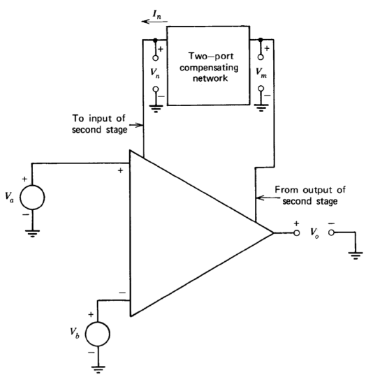
Figure 13.11 Operational amplifier compensated with a two-port network.
Figure 13.11 illustrates the topology for an amplifier compensated with a two-port network. This basic configuration has been described earlier in Sections 5.3 and 9.2.3. While the exact details depend on specifics of the amplifier involved, the important general conclusions introduced in the earlier material include the following:
(a) The unloaded open-loop transfer function of a two-stage amplifier compensated this way (assuming that the minor loop is stable) is
\[a(s) = \dfrac{V_o (s)}{V_a (s) - V_b (s)} \simeq \dfrac{K}{Y_c (s)} \label{eq13.3.1} \]
over a wide range of frequencies.
The quantity \(K\) is related to the transconductance of the input-stage transistors, while \(Y_c (s)\) is the short-circuit transfer admittance of the network.
\[Y_c (s) = \dfrac{I_n (s)}{V_m (s)} |_{V_n = 0} \nonumber \]
This result can be justified by physical reasoning if we remember that at frequencies where the transmission of the minor loop formed by the second stage and the compensating network is large, the input to the second stage is effectively a virtual incremental ground. Furthermore, the current required at the input to the second stage is usually very small. Thus it can be shown by an argument similar to that used to determine the ideal closed-loop gain of an operational amplifier that incremental changes in current from the input stage must be balanced by equal currents into the compensating network. System parameters are normally selected so that major-loop crossover occurs at frequencies where the approximation of Equation \(\ref{eq13.3.1}\) is valid and, therefore, this approximation can often be used for stability calculations.
(b) The d-c open-loop gain of the amplifier is normally independent of compensation. Accordingly, at low frequencies, the approximation of Equation \(\ref{eq13.3.1}\) is replaced by the constant value ao. The approximation fails because
the usual compensating networks include a d-c zero in their transfer admittances, and at low frequencies this zero decreases the magnitude of the minor-loop transmission below one.
(c) The approximation fails at high frequencies for two reasons. The minor-loop transmission magnitude becomes less than one, and thus the network no longer influences the transfer function of the second stage. This transfer function normally has at least two poles at high frequencies, reflecting capacitive loading at the input and output of the second stage. There may be further departure from the approximation because of singularities associated with the input stage and the buffer stage that follows the second stage. These singularities cannot be controlled by the minor loop since they are not included in it.
(d) The open-loop transfer function of the compensated amplifier can be estimated by plotting both the magnitude of the approximation (Equation \(\ref{eq13.3.1}\)) and of the uncompensated amplifier transfer function on common log-magnitude versus log-frequency coordinates. If the dominant amplifier dynamics are associated with the second stage, the compensated open-loop transfer-function magnitude is approximately equal to the lower of the two curves at all frequencies. The uncompensated amplifier transfer function must reflect loading by the compensating network at the input and the output of the second-stage. In practice, designers usually determine experimentally the frequency range over which the approximation of Equation \(\ref{eq13.3.1}\) is valid for the amplifier and compensating networks of interest.
Several different types of compensation are described in the following sections. These compensation techniques are illustrated using an LM301A operational amplifier. This inexpensive, popular amplifier is the commercial-temperature-range version of the LM1OA amplifier described in Section 10.4.1. Recall from that discussion that the quantity \(K\) is nominally \(2 \times 10^4\) mho for this amplifier, and that its specified d-c open-loop gain is typically 160,000. Phase shift from elements outside the minor loop (primarily the lateral-PNP transistors in the input stage) becomes significant at 1 MHz, and feedback connections that result in a crossover frequency in excess of approximately 2 MHz generally are unstable.
A number of oscilloscope photographs that illustrate various aspects of amplifier performance are included in the following material. A single LM301A was used in all of the test circuits. Thus relative performance reflects differences in compensation, loading, and feedback, but not in the uncompensated properties of the amplifier itself. (The fact that this amplifier survived the abuse it received by being transferred from one test circuit to another and during testing is a tribute to the durability of modern integrated-circuit operational amplifiers.)
One-Pole Compensation
The most common type of compensation for two-stage amplifiers involves the use of a single capacitor between the compensating terminals. Since the short-circuit transfer admittance of this "network" is \(C_c s\) where \(C_c\), is the value of the compensating capacitor, Equation \(\ref{eq13.3.1}\) predicts
\[a(s) \simeq \dfrac{K}{C_c s}\label{eq13.3.3} \]
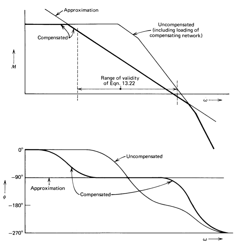
Figure 13.12 Open-loop transfer function for one-pole compensation.
The approximation of Equation \(\ref{eq13.3.3}\) is plotted in Figure 13.12 along with a representative uncompensated amplifier transfer function. As explained in the previous section, the compensated open-loop transfer function is very nearly equal to the lower of the two curves at all frequencies.
The important feature of Figure 13.12, which indicates the general-purpose nature of this type of one-pole compensation, is that there is a wide range of frequencies where the magnitude of \(a(j\omega)\) is inversely proportional to frequency and where the angle of this open-loop transfer function is approximately \(-90^{\circ}\). Accordingly, the amplifier exhibits essentially identical stability (but a variable speed of response) for many different values of frequency-independent feedback connected around it.
Two further characteristics of the open-loop transfer function of the amplifier are also evident from Figure 13.12. First, the approximation of Equation \(\ref{eq13.3.3}\) can be extended to zero frequency if the d-c open-loop gain of the amplifier is known, since the geometry of Figure 13.12 shows that
\[a(s) \simeq \dfrac{a_0}{(a_0 C_c/K)s + 1} \nonumber \]
at low and intermediate frequencies. Second, if the unity-gain frequency of the amplifier is low enough so that higher-order singularities are unimportant, this frequency is inversely related to \(C_c\) and is
\[\omega_u = \dfrac{K}{C_c} \nonumber \]
Stability calculations for feedback connections that use this type of amplifier are simplified if we recognize that provided the crossover frequency of the combination lies in the indicated region, these calculations can be based on the approximation of \(\ref{eq13.3.3}\).
Several popular internally compensated amplifiers such as the LM107 and the \(\mu A741\) combine nominal values of \(K\) of \(2 \times 10^{-4}\) mho with \(30-pF\) capacitors for \(C_c\). The resultant unity-gain frequency is \(6.7 \times 10^6\) radians per second or approximately 1 MHz. This value insures stability for any resistive feedback networks connected around the amplifier, since, with this type of feedback, crossover always occurs at frequencies where the loop transmission is dominated by one pole.
The approximate open-loop transfer function for either of these internally compensated amplifiers is \(a(s) = 6.7 \times 10^6/s\). This transfer function, which is identical to that obtained from an LM101A compensated with a \(30-pF\) capacitor, may be optimum in applications that satisfy the following conditions:
(a) The feedback-network transfer function from the amplifier output to its inverting input has a magnitude of one at the amplifier unity-gain frequency.
(b) Any dynamics associated with the feedback network and output loading contribute less than \(30^{\circ}\) of phase shift to the loop transmission at the crossover frequency.
(c) Moderately well-damped transient response is required.
(d) Input signals are relatively noise free.
If one or more of the above conditions are not satisfied, performance can often be improved by using an externally compensated amplifier that allows flexibility in the choice of compensating-capacitor value. Consider, for example, a feedback connection that combines \(a(s)\) as approximated by Equation \(\ref{eq13.3.3}\) with frequency-independent feedback \(f_0\). The closed-loop transfer function for this combination is
\[A(s) = \dfrac{a(s)}{1 + a(s) f_0} = \dfrac{1}{f_0} \left [\dfrac{1}{(C_c/Kf_0)s + 1} \right ] \label{eq13.3.6} \]
The closed-loop corner frequency (in radians per second) is
\[\omega_h = \dfrac{Kf_0}{C_c} \nonumber \]
This equation shows that the bandwidth can be maintained at the maximum value consistent with satisfactory stability (recall the phase shift of terms ignored in the approximation of Equation \(\ref{eq13.3.3}\)) if \(C_c\) is changed with \(f_0\) to keep the ratio of these two quantities constant. Alternatively, the closed-loop bandwidth can. be lowered to provide improved filtering for noisy input signals by increasing the size of the compensating capacitor. A similar increase in capacitor size can also force crossover at lower frequencies to keep poles associated with the load or a frequency-dependent feedback network from deteriorating stability.
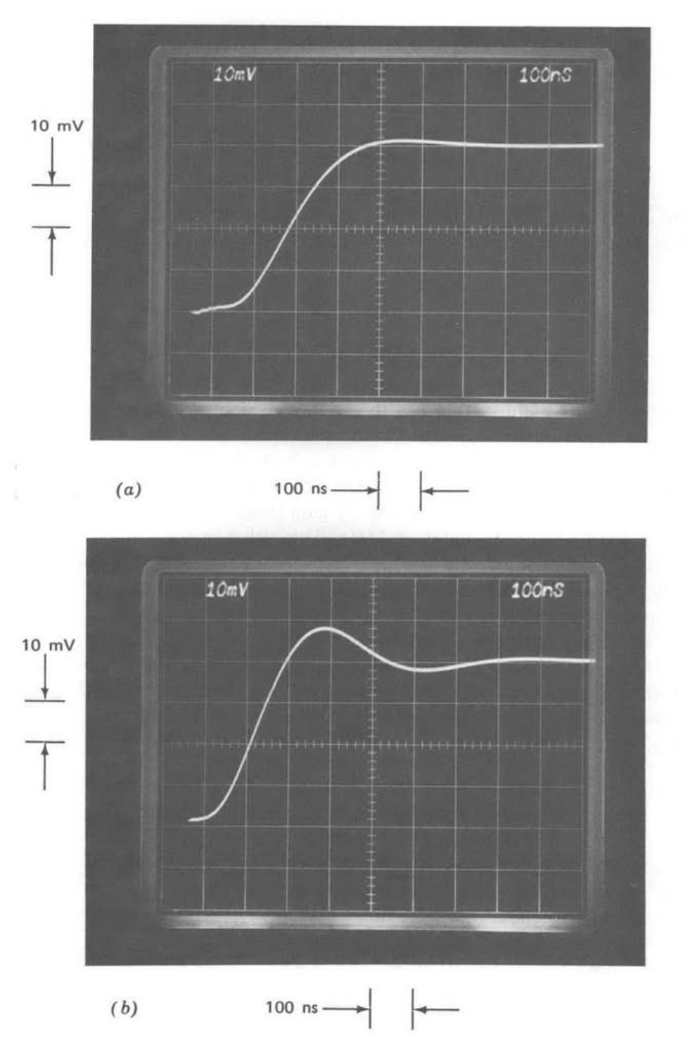
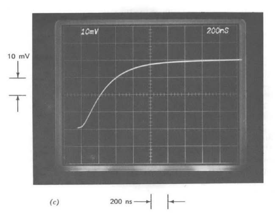
Figure 13.13 Step response of unity-gain follower as a function of compensating-capacitor value. (Input-step amplitude is \(40\ mV\). (\(a\)) \(C_c = 30\ pF\). (\(b\)) \(C_c = 18\ pF\). (\(c\)) \(C_c = 68\ pF\).
Figure 13.13 shows the small-signal step responses for the LM301A test amplifier connected as a unity-gain follower (\(f_0 = 1\)). Part a of this figure
illustrates the response with a \(30-pF\) compensating capacitor, the value used in similar, internally compensated designs. This transient response is quite well damped, with a 10 to 90% rise time of 220 ns, implying a closed-loop bandwidth (from Equation 3.5.7) of approximately \(10^7\) radians per second or 1.6 MHz.(If the amplifier open-loop transfer function were exactly first order, the closed-loop half-power frequency in this connection would be identically equal to the unity-gain frequency of the amplifier itself. However, the phase shift of higher-frequency singularities ignored in the one-pole approximation introduces closed-loop peaking that extends the closed-loop bandwidth.)
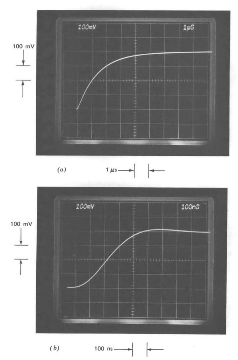
The response with a \(18-pF\) compensating capacitor (Figure 13.13\(b\)) trades considerably greater overshoot for improved rise time. Comparing this response with the second-order system responses (Figure 3.8) shows that the
closed-loop transient is similar to that of a second-order system with 0.47 and \(\omega_n = 13.5 \times 10^6\) radians per second. Since the amplifier open-loop transfer function satisfies the conditions used to develop the curves of Figure 4.26, we can use these curves to approximate loop-transmission properties. Figure Figure 4.26a estimates a phase margin of \(50^{\circ}\) and a crossover frequency of \(11 \times 10^6\) radians per second. Since the value of \(f\) is one in this connection, these quantities correspond to compensated open-loop parameters of the amplifier itself.
Figure 13.13\(c\) illustrates the step response with a \(68-pF\) compensating capacitor. The response is essentially first order, indicating that crossover now occurs at a frequency where only the dominant pole introduced by compensation is important. Equation \(\ref{eq13.3.6}\) predicts an exponential time constant
\[\tau = \dfrac{C_c}{Kf_0} \label{eq13.3.8} \]
under these conditions. The zero to 63% rise time shown in Figure 13.12\(c\) is approximately 300 ns. Solving Equation \(\ref{eq13.3.8}\) for \(K\) using known parameter values yields
\[K = \dfrac{C_c}{\tau f_0} = \dfrac{68\ pF}{300\ ns} = 2.3 \times 10^{-4} \text{ mho}\label{eq13.3.9} \]
We notice that this value for \(K\) is slightly higher than the nominal value of \(2 \times 10^{-4}\text{ mho}\), reflecting (in addition to possible experimental errors) a somewhat higher than nominal first-stage quiescent current for this particular amplifier.(The quiescent first-stage current of this amplifier can be measured directly by connecting an ammeter from terminals 1 and 5 to the negative supply (see Figure 10.19). The estimated value of \(K\) is in excellent agreement with the measured total (the sum of both sides) quiescent current of \(24\mu A\) for the test amplifier.) Variations of as much as 50% from the nominal value for \(K\) are not unusual as a consequence of uncertainties in the integrated- circuit process.
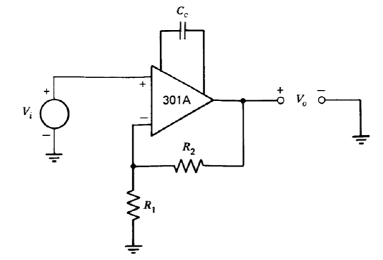
Figure 13.14 Noninverting amplifier.
The amplifier was next connected in the noninverting configuration shown in Figure 13.14. The value of \(R_1\) was kept less than or equal to \(1\ k\Omega\) in all connections to minimize the loading effects of amplifier input capacitance. Figure 13.15\(a\) shows the step response for a gain-of-ten connection (\(R_1 = 1\ k\Omega, R_2 = 9\ k\Omega\)) with \(C_c = 30\ pF\). The 10 to 90% rise time has increased significantly compared with the unity-gain case using identical compensation. This change is expected because of the change in fo (see Equation \(\ref{eq13.3.6}\)).
Figure 13.15\(b\) is the step response when the capacitor value is lowered to get an overshoot approximately equal to that shown in Figure 13.13\(a\). While this change does not return rise time to exactly the same value displayed in Figure 13.13\(a\), the speed is dramatically improved compared to the transient shown in Figure 13.15\(a\). (Note the difference in time scales.)
Our approximate relationships predict that the effects of changing fo from 1 to 0.1 could be completely offset by lowering the compensating capacitor from \(30\ pF\) to \(3\ pF\). The actual capacitor value required to obtain the response shown in Figure 13.15\(b\) was approximately \(4.5\ pF\). At least two effects contribute to the discrepancy. First, the approximation ignores higher-frequency open-loop poles, which must be a factor if there is any overshoot in the step response. Second, there is actually some positive minor-loop capacitive feedback in the amplifier. The schematic diagram for the LM101A (Figure 10.19) shows that the amplifier input stage is loaded with a current repeater. The usual minor-loop compensation is connected to the output side of this current repeater. However, the input side of the
repeater is also brought out on a pin to be used for balancing the amplifier. Any capacitance between a part of the circuit following the high-gain stage and the input side of the current repeater provides positive minor-loop feedback because of the inversion of the current repeater. An excellent stray-capacitance path exists between the amplifier output (pin 6) and the balance terminal connected to the input side of the current repeater (pin 5).(A wise precaution that reduces this effect is to clip off pin 5 close to the can when the amplifier is used in connections that do not require balancing. This modification was not made to the demonstration amplifier in order to retain maximum flexibility. Even with pin 5 cut close to the can, there is some header capacitance between it and pin 6.) Part of the normal compensating capacitance is "lost" cancelling this positive feedback capacitance.
The important conclusion to be drawn from Figure 13.15 is that, by properly selecting the compensating-capacitor value, the rise time and bandwidth of the gain-of-ten amplifier can be improved by approximately a factor of 10 compared to the value that would be obtained from an amplifier with fixed compensation. Furthermore, reasonable stability can be retained with the faster performance.
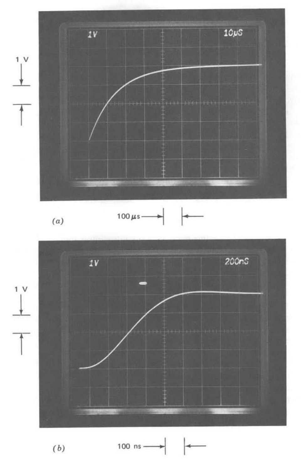
Figure 13.16 Step responses of gain-of-100 noninverting amplifier. (Input-step amplitude is \(40\ mV\).) (\(a\)) \(C_c = 30\ pF\). (\(b\)) \(C_c = 1\ pF\).
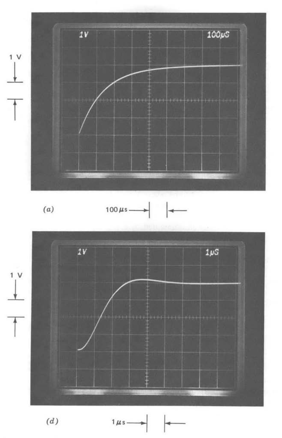
Figure 13.17 Step responses of gain-of-1000 noninverting amplifier. (Input-step amplitude is \(4\ mV\).) (\(a\)) \(C_c = 30\ pF\). (\(b\)) Very small \(C_c\).
Figures 13.16 and 13.17 continue this theme for gain-of-100 (\(R_1 = 100\ \Omega, R_2 = 10\ k\Omega\)) and gain-of-1000 (\(R_1 = 10\ \Omega, R_2 = 10\ k\Omega\)) connections, respectively. The rise time for \(30-pF\) compensation is linearly related to gain, and has a 10 to 90% value of approximately 350 microseconds in Figure 13.17\(a\), implying a closed-loop bandwidth of 1 kHz for an internally compensated amplifier in this gain-of-1000 connection. Compensating-capaci tor values of \(1\ pF\) for the gain-of-100 amplifier and just a pinch (obtained with two short, parallel wires spaced for the desired transient response) for the gain-of-1000 connection result in overshoot comparable to that of the unity-gain follower compensated with \(30\ pF\). The rise time does increase slightly at higher gains reflecting the fact that the uncompensated amplifier high-frequency open-loop gain is limited. However, a rise time of approximately 2 us is obtained in the gain-of-1000 connection. The corresponding closed-loop bandwidth of 175 kHz represents a nearly 200:1 improvement compared with the value expected from an internally compensated general- purpose amplifier.
It is interesting to note that the closed-loop bandwidth obtained by properly compensating the inexpensive LM301A in the gain-of-1000 connection compares favorably with that possible from the best available discrete-component, fixed-compensation operational amplifiers. Unity-gain frequencies for wideband discrete units seldom exceed 100 MHz; consequently these single-pole amplifiers have closed-loop bandwidths of 100 kHz or less in the gain-of-1000 connection. The bandwidth advantage compared with wideband internally compensated integrated-circuit amplifiers such as the LM 118 is even more impressive.
We should realize that obtaining performance such as that shown in Figure 13.17\(b\) requires careful adjustment of the compensating-capacitor value because the optimum value is dependent on the characteristics of the particular amplifier used and on stray capacitance. Although this process is difficult in a high-volume production situation, it is possible, and, when all costs are considered, may still be the least expensive way to obtain a high-gain wide-bandwidth circuit. Furthermore, compensation becomes routine if some decrease in bandwidth below the maximum possible value is acceptable.
Two-pole Compensation
The one-pole compensation described above is a conservative, general-purpose compensation that is widely used in a variety of applications. There are, however, many applications where higher desensitivity at intermediate frequencies than that afforded by one-pole magnitude versus frequency characteristics is advantageous. Increasing the intermediate-frequency magnitude of a loop transmission dominated by a single pole necessitates a corresponding increase in crossover frequency. This approach is precluded in systems where irreducible phase shift constrains the maximum crossover frequency for stable operation.
The only way to improve intermediate-frequency desensitivity without increasing the crossover frequency is to use a higher-order loop-transmission rolloff at frequencies below crossover. For example, consider the two amplifier open-loop transfer functions
\[a(s) = \dfrac{10^5}{10^{-2} s + 1}\label{eq13.3.10} \]
and
\[a'(s) = \dfrac{10^5 (10^{-6} s + 1)}{(10^{-4} s + 1)^2}\label{eq13.3.11} \]
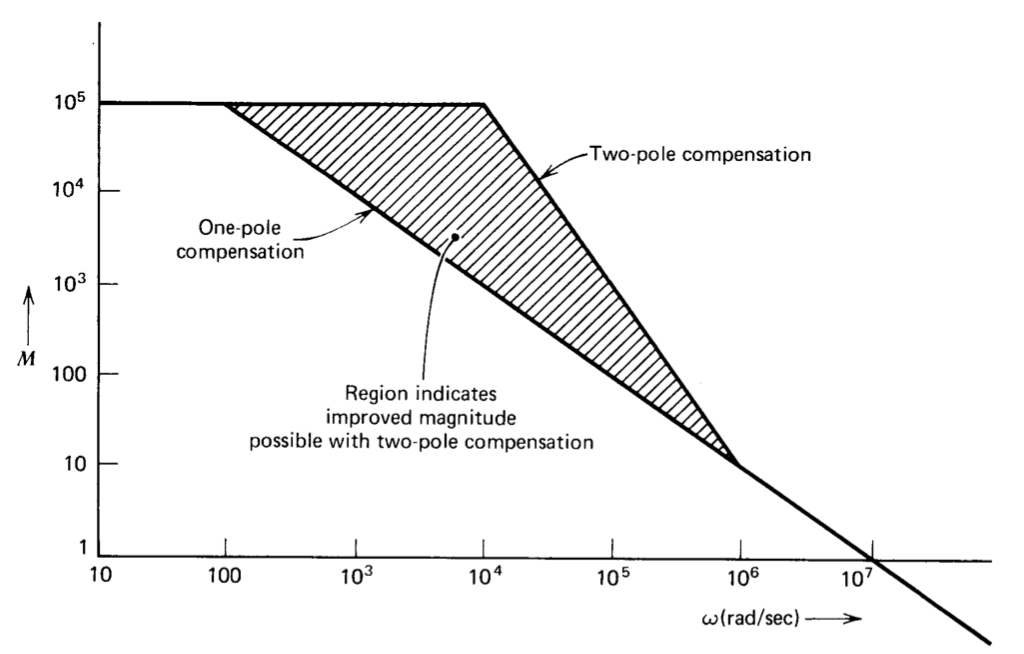
Figure 13.18 Comparison of magnitudes of one- and two-pole open-loop transfer functions.
The magnitude versus frequency characteristics of these two transfer functions are compared in Figure 13.18.
Both of these transfer functions have unity-gain frequencies of \(10^7\) radians per second and d-c magnitudes of 105. However, the magnitude of \(a'(j\omega )\) exceeds that of \(a(j\omega )\) at all frequencies between 100 radians per second and \(10^6\) radians per second. The advantage reaches a factor of 100 at \(10^4\) radians per second.
The same advantage can be demonstrated using error coefficients. If amplifiers with open-loop transfer functions given by Equations \(\ref{eq13.3.10}\) and \(\ref{eq13.3.11}\) are connected as unity-gain followers, the respective closed-loop gains are
\[A(s) = \dfrac{a(s)}{1 + a(s)} = \dfrac{10^5}{10^{-2}s + 1 + 10^5} \nonumber \]
and
\[A'(s) = \dfrac{a'(s)}{1 + a'(s)} = \dfrac{10^5 (10^{-6} s + 1)}{(10^{-4} s + 1)^2 + 10^5 (10^{-6} s + 1)} \nonumber \]
The corresponding error series are
\[1 - A(s) \simeq \dfrac{10^{-2} s + 1}{10^{-2} s + 10^5} = 10^{-5} + 10^{-7} s - \cdots + \nonumber \]
and
\[1 - A'(s) \simeq \dfrac{10^{-8} s^2 + 2 \times 10^{-4} s + 1}{10^{-8} s^2 + 0.1 s + 10^5} = 10^{-5} + 2 \times 10^{-9} s + \cdots + \nonumber \]
Identifying error coefficients shows that while these two systems have identical values for \(e_0\), the error coefficient ei is a factor of 50 times smaller for the system with the two-pole rolloff. Thus, dramatically smaller errors result with the two-pole system for input signals that cause the \(e_1\) term of the error series to dominate.

Figure 13.19 Network for two-pole compensation.
It is necessary to use a true two-port network to implement this compensation, since the required \(s^2\) dependence of \(Y_c\) cannot be obtained with a two-terminal network. The short-circuit transfer admittance of the net work shown in Figure 13.19,
\[\dfrac{I_n (s)}{V_n (s)} = \dfrac{RC_1 C_2 s^2}{R(C_1 + C_2)s + 1} \nonumber \]
has the required form. The approximate open-loop transfer function with this type of compensating network is (from Equation \(\ref{eq13.3.1}\))
\[a(s) \simeq \dfrac{K}{Y_c} \simeq \dfrac{K'(\tau s + 1)}{s^2} \label{eq13.3.17} \]
where \(\tau = R(C_1 + C_2)\) and \(K' = K/RC_1C_2\).
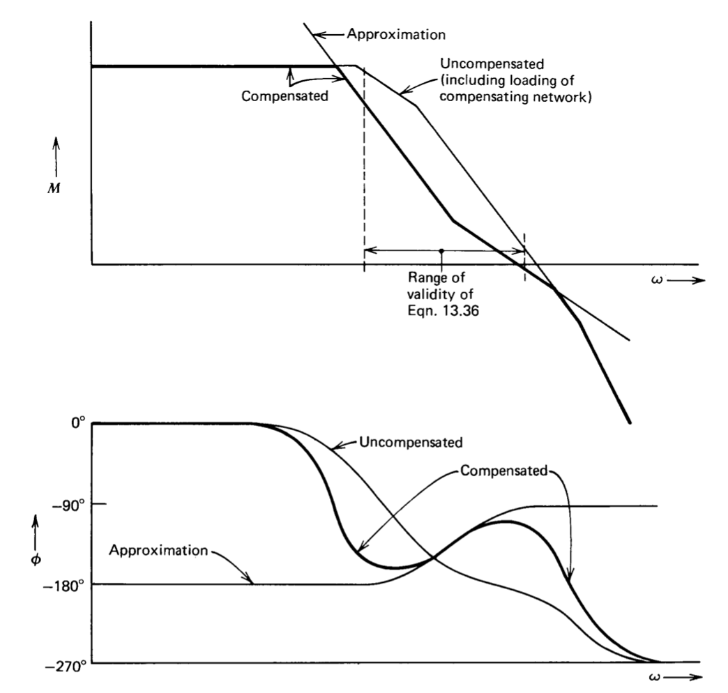
Figure 13.20 Open-loop transfer function for two-pole compensation.
An estimation of the complete open-loop transfer function based on Equation \(\ref{eq13.3.17}\) and a representative uncompensated transfer function are shown in Figure 13.20. We note that while this type of transfer function can yield significantly improved desensitivity and error-coefficient magnitude compared to a one-pole transfer function, it is not a general-purpose compensation. The zero location and constant \(K'\) must be carefully chosen as a function of the attenuation provided by the feedback network in a particular application in order to obtain satisfactory phase margin. While lowering the frequency of the zero results in a wider frequency range of acceptable phase margin, it also reduces desensitivity, and in the limit leads to a one-pole transfer function. This type of open-loop transfer function is also intolerant of an additional pole introduced in the feedback network or by capacitive loading. If the additional pole is located at an intermediate frequency below the zero location, instability results. Another problem is that
there is a wide range of frequencies where the phase shift of the transfer function is close to - 1800. While this transfer function is not conditionally stable by the definition given in Section 6.3.4, the small phase margin that results when the crossover frequency is lowered (in a describing-function sense) by saturation leads to marginal performance following overload.
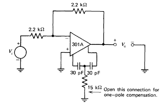
Figure 13.21 Unity-gain inverter with two-pole compensation.
In spite of its limitations, two-pole compensation is a powerful technique for applications where signal levels and the dynamics of additional elements in the loop are well known. This type of compensation is demonstrated using the unity-gain inverter shown in Figure 13.21. The relatively low feedback-network resistors are chosen to reduce the effects of capacitance at the inverting input of the amplifier. This precaution is particularly important since the voltage at this input terminal is displayed in several of the oscilloscope photographs to follow. An LM310 voltage follower (see Section 10.4.4) was used to isolate this node from the relatively high oscilloscope input capacitance for these tests. The input capacitance of the LM310 is considerably lower than that of a unity-gain passive oscilloscope probe, and its bandwidth exceeds that necessary to maintain the fidelity of the signal of interest.
The approximate open-loop transfer function for the amplifier with compensating-network values as shown in Figure 13.21 is (from Equation \(\ref{eq13.3.17}\) using the previously determined value of \(K = 2.3 \times 10^{-4}\) mho)
\[a(s) \simeq \dfrac{1.7 \times 10^{13} (9\times 10^{-7} s + 1)}{s^2}\label{eq13.3.18} \]
Since the value of \(f_0\) for the unity-gain inverter is 1/2, the approximate loop transmission for this system is
\[L(s) \simeq - \dfrac{0.85 \times 10^{13} (9 \times 10^{-7} s + 1)}{s^2}\label{eq13.3.19} \]
The crossover frequency predicted by Equation \(\ref{eq13.3.19}\) is \(7.7 \times 10^6\) radians per second, and the zero is located at \(1.1 \times 10^6\) radians per second, or a factor of 7 below the crossover frequency. Consequently, the phase margin of this system is \(\tan^{-1} (1/7) = 8^{\circ}\) less than that of a unity-gain inverter using one-pole compensation adjusted for the same crossover frequency.
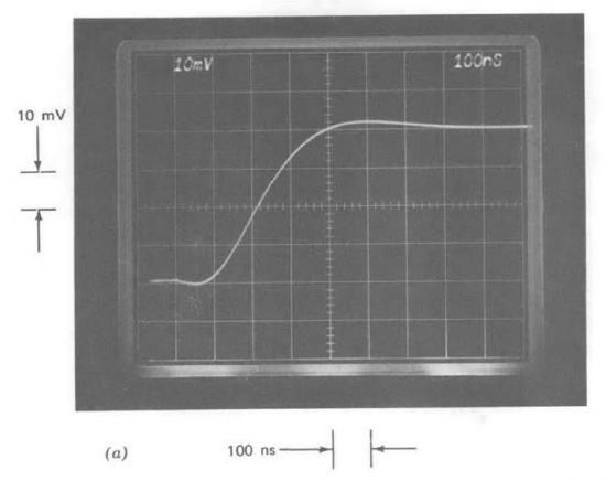
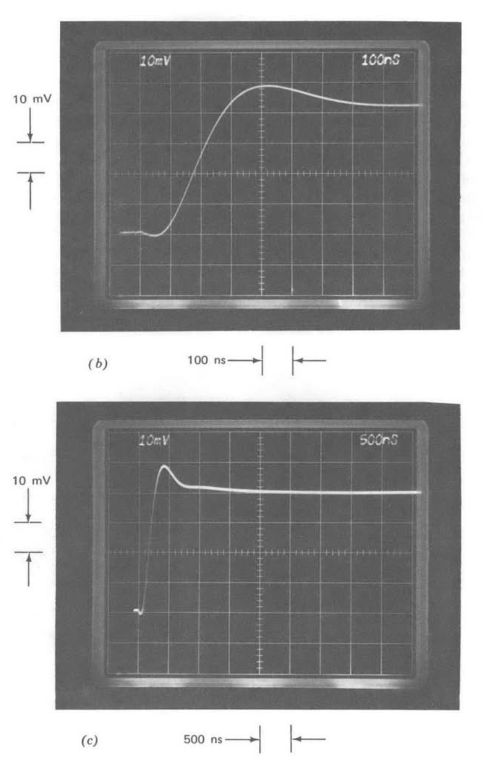
Figure 13.22 Step responses of unity-gain inverter. (Input-step amplitude is \(-40\ mV\).) (\(a\)) One-pole compensation. (\(b\)) Two-pole compensation. (\(c\)) Repeat of part \(b\) with slower sweep speed.
Figure 13.22 compares the step responses of the inverter-connected LM301A with one- and two-pole compensation. Part a of this figure was obtained with the lower end of the \(15-k\Omega\) resistor removed from ground as indicated in Figure 13.21. In this case the compensating element is equivalent to a single \(15-pF\) capacitor. Note that Equation \(\ref{eq13.3.3}\) combined with the value \(f_0 = 1/2\), which applies to the unity-gain inverter, predicts a \(7.7 \times 10^6\)-radian-per-second crossover frequency for \(15-pF\) compensation. The same result can be obtained by realizing that at frequencies beyond the zero location the parallel impedance of the capacitors in the two-pole compensating network must be smaller than that of the resistor, and thus removing the resistor does not alter the amplifier open-loop transfer function substantially in the vicinity of crossover.
The response shown in Figure 13.22\(a\) is quite similar to that shown previously in Figure 13.13\(a\). Recall that Figure 13.13\(a\) was obtained with a unity-gain follower (\(f_0 = 1\)) and \(C_c = 30\ pF\). As anticipated, lowering \(f_0\) and \(C_c\) by the same factor results in comparable performance for single-pole systems.
There is a small amount of initial undershoot evident in the transient of Figure 13.22\(a\). This undershoot results from the input step being fed directly to the output through the two series-connected resistors. This fed-forward signal can drive the output negative initially because of the nonzero output impedance and response time of the amplifier. The magnitude of the initial undershoot would shrink if larger-value resistors were used around the amplifier.
The step response of Figure 13.22\(b\) results with the \(15-k\Omega\) resistor connected to ground and is the response for two-pole compensation. Three effects combine to speed the rise time and increase the overshoot of this response compared to the single-pole case. First, the phase margin is approximately 80 less for the two-pole system. Second, the \(T\) network used for two-pole compensation loads the output of the second stage of the amplifier to a greater extent than does the single capacitor used for one-pole compensation, although this effect is small for the element values used in the present example. The additional loading shifts the high-frequency poles associated with limited minor-loop transmission toward lower frequencies. Third, a closed-loop zero that results with two-pole compensation also influences system response.
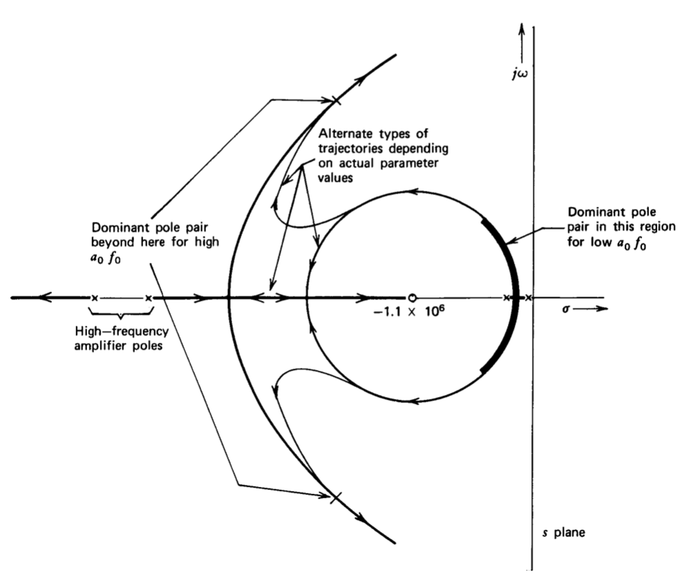
Figure 13.23 Root-locus diagram for inverter with two-pole compensation.
The root-locus diagram shown in Figure 13.23 clarifies the third reason. (Note that this diagram is not based on the approximation of Equation \(\ref{eq13.3.19}\), but rather on a more complete loop transmission assuming a representative amplifier using these compensating-network values.) With the value of \(a_0f_0\) used to obtain Figure 13.22\(b\), one closed-loop pole is quite close to the zero at \(- 1.1 \times 10^6\text{ sec}^{-1}\) regardless of the exact details of the diagram. Since the zero is in the forward path of the system, it appears in the closed-loop transfer function. The resultant closed-loop doublet adds a positive, long-duration "tail" to the response as explained in Section 5.2.6. The tail is clearly evident in Figure 13.22\(c\), a repeat of part \(b\) photographed with a slower sweep speed. The time constant of the tail is consistent with the doublet location at approximately \(- 10^6\text{ sec}^{-1}\).
We recall that this type of tail is characteristic of lag-compensated systems. The loop transmission of the two-pole system combines a long \(1/s^2\) region with a zero below the crossover frequency. This same basic type of loop transmission results with lag compensation.
The root-locus diagram also shows that satisfactory damping ratio is obtained only over a relative small range of \(a_0f_0\). As \(a_0f_0\) falls below the optimum range, system performance is dominated by a low-frequency poorly damped pole pair as indicated in Figure 13.23. As \(a_0f_0\) is increased above the optimum range, a higher-frequency poorly damped pole pair dominates performance since the real-axis pole closest to the origin is very nearly cancelled by the zero.
The error-reducing potential of two-pole compensation is illustrated in Figure 13.24. The most important quantity included in these photographs is the signal at the inverting input of the operational amplifier. The topology used (Figure 13.21) shows that the signal at this terminal is (in the absence of loading) half the error between the actual and the ideal amplifier output.
Part a of this figure indicates performance with single-pole compensation achieved via a \(15-pF\) capacitor. The upper trace indicates the.amplifier output when the signal applied from the source is a 20-volt peak-to-peak, 10-kHz triangle wave. This signal is, to within the resolution of the measurement, the negative of the signal applied by the source. The bottom trace is the signal at the inverting input terminal of the operational amplifier.
The approximate open-loop transfer function from the inverting input to the output of the test amplifier is
\[-a(s) = -\dfrac{2.3 \times 10^{-3}}{1.5 \times 10^{-11} s} = -\dfrac{1.5 \times 10^7}{s}\label{eq13.3.20} \]
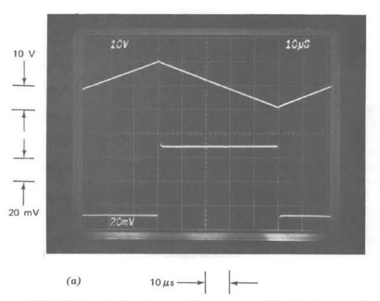
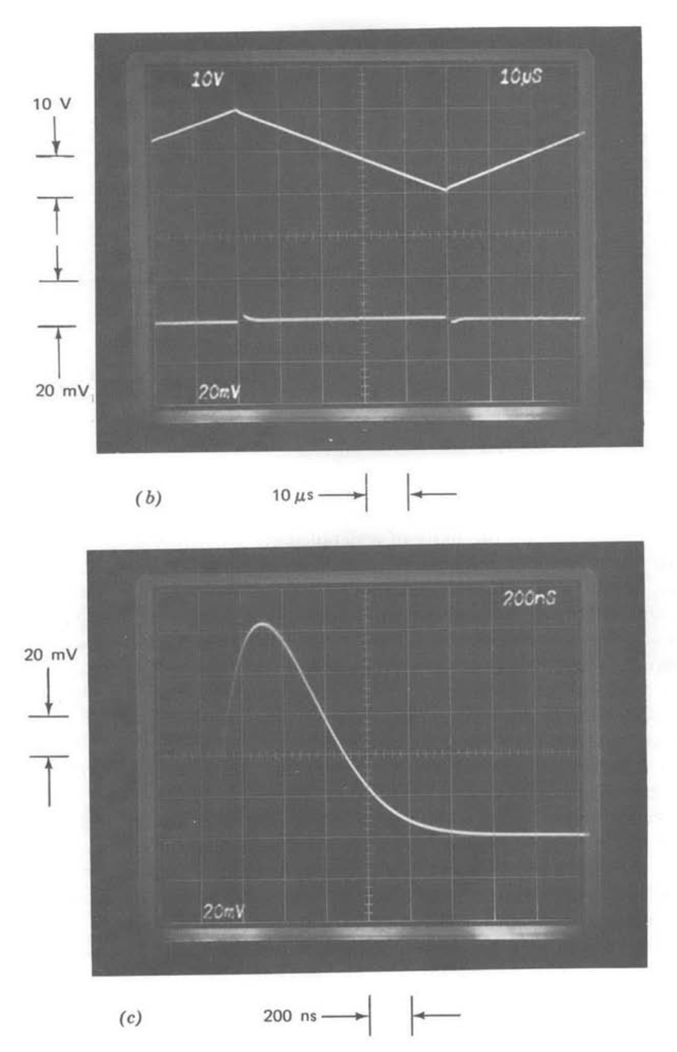
Figure 13.24 Unity-gain inverting-amplifier response with triangle-wave input. (Input amplitude is 20 volts peak-to-peak.) (\(a\)) One-pole compensation-upper trace: output; lower trace: inverting input of operational amplifier. (\(b\)) Two-pole compensation-upper trace: output; lower trace: inverting input of operational amplifier. (\(c\)) Repeat of lower trace, part \(b\), with faster sweep speed.
with a \(15-pF\) compensating capacitor. The input-terminal signal illustrated can be justified on the basis of a detailed error-coefficient analysis using this value for \(a(s)\). A simplified argument, which highlights the essential feature of the error coefficients for this type of compensation, is to recognize that Equation \(\ref{eq13.3.20}\) implies that the operational amplifier itself functions as an integrator on an open-loop basis. Since the amplifier output signal is a triangle wave, the signal at the inverting input terminal (proportional to the derivative of the output signal) must be a square wave. The peak magnitude of the square wave at the input of the operational amplifier should be the magnitude of the slope of the output, \(4 \times 10^5\) volts per second, divided by the scale factor \(1.5 \times 10^7\) volts per second per volt from Equation \(\ref{eq13.3.20}\), or approximately \(27\ mV\). This value is confirmed by the bottom trace in Figure 13.24\(a\) to within experimental errors.
Part b of Figure 13.24 compares the output signal and the signal applied to the inverting input terminal of the operational amplifier with the two-pole compensation described earlier. A substantial reduction in the amplifier input signal, and thus in the error between the actual and ideal output, is clearly evident with this type of compensation. There are small-area error pulses that occur when the triangle wave changes slope. These pulses are difficult to observe in Figure 13.24\(b\). The time scale is changed to present one of these error pulses clearly in Figure 13.24\(c\). Note that this pulse is effectively an impulse compared to the time scale of the output signal. As might be anticipated, when compensation that makes the amplifier behave like a double integrator is used, the signal at the amplifier input is approximately the second derivative of its output, or a train of alternating-polarity im pulses.
Equation \(\ref{eq13.3.18}\) shows that
\[a(s) \simeq \dfrac{1.7 \times 10^{13}}{s^2}\label{eq13.3.21} \]
at frequencies below approximately 106 radians per second for the two-pole compensation used. A graphically estimated value for the area of the impulse shown in Figure 13.24\(c\) is \(5 \times 10^{-8}\) volt-seconds. Multiplying this area by the scale factor \(1.7 \times 10^{13}\) volts per second squared per volt from Equation \(\ref{eq13.3.21}\) predicts a change in slope of \(8.5 \times 10^5\) volts per second at each break of the triangle wave. This value is in good agreement with the actual slope change of \(8 \times 10^5\) volts per second.
We should emphasize that the comparisons between one- and two-pole compensation presented here were made using one-pole compensation tailored to the attenuation of the feedback network. Had the standard \(30-pF\) compensating-capacitor value been used, the error of the one-pole compensated configuration would have been even larger.
Compensation That Includes a Zero
We have seen a number of applications where the feedback network or capacitive loading at the output of the operational amplifier introduces a pole into the loop transmission. This pole, combined with the single dominant pole often obtained via minor-loop compensation, will deteriorate stability.
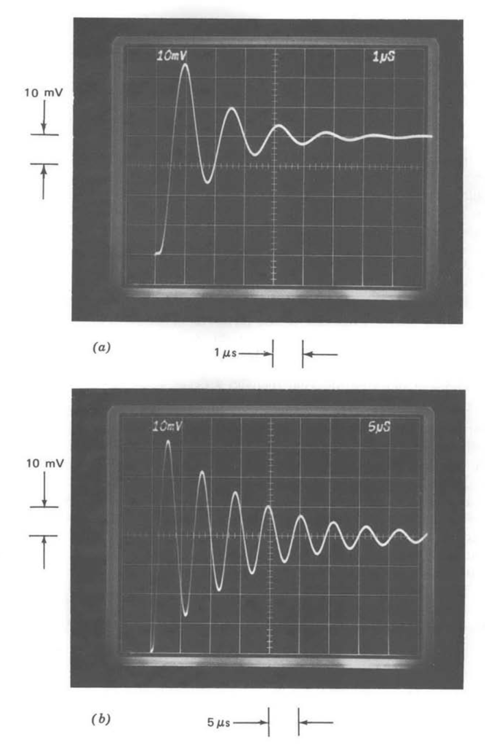
Figure 13.25 Step response of capacitively loaded unity-gain follower with one-pole compensation. (Input-step amplitude is \(40\ mV\).) (a) \(0.01-\mu F\) load capacitor. (\(b\)) \(0.1-\mu F\) load capacitor.
Figure 13.25 shows how capacitive loading decreases the stability of the LM301A when single-pole compensation is used. The amplifier was connected as a unity-gain follower and compensated with a single \(30-pF\) capacitor to obtain these responses. The load-capacitor values used were \(0.01\ \mu F\) and \(0.1\ pF\) for parts \(a\) and \(b\), respectively.
These transient responses can be used to estimate the open-loop output resistance of the operational amplifier. We know that the open-loop transfer function for this amplifier compensated with a \(30-pF\) capacitor is
\[a(s) \simeq \dfrac{7.7 \times 10^6}{s} \nonumber \]
in the absence of loading. This transfer function is also the negative of the unloaded loop transmission for the follower connection. When capacitive loading is included, the loop transmission changes to
\[L(s) \simeq -\dfrac{7.7 \times 10^6}{s(R_o C_L s + 1)}\label{eq13.3.23} \]
where \(R_o\) is the open-loop output resistance of the amplifier and \(C_L\) is the value of the load capacitor.
The ringing frequency shown in Figure 13.25\(b\) is approximately \(1.1 \times 10^6\) radians per second. Since this response is poorly damped, the ringing frequency must closely approximate the crossover frequency. Furthermore, the poor damping also indicates that crossover occurs well above the break frequency of the second pole in Equation \(\ref{eq13.3.23}\).
These relationships, combined with the known value for \(C_L\), allow Equation \(\ref{eq13.3.23}\) to be solved for \(R_o\), with the result
\[R_o \simeq \dfrac{7.7 \times 10^6}{\omega_c^2 C_L} = 65\ \Omega \lable{eq13.3.24} \nonumber \]
One simple way to improve stability is to include a zero in the unloaded open-loop transfer function of the amplifier to partially offset the negative phase shift of the additional pole in the vicinity of crossover. If a series resistor-capacitor network with component values \(R_c\) and \(C_c\) is used for compensation, the short-circuit transfer admittance of the network is
\[Y_c = \dfrac{C_c s}{R_c C_c s + 1} \nonumber \]
The approximate value for the corresponding unloaded open-loop transfer function of the amplifier is
\[a(s) \simeq \dfrac{K(R_c C_c s + 1)}{C_c s} \lable{eq13.3.26} \nonumber \]
Figure 13.26 Unloaded open-loop transfer function for compensation that includes a zero.
An estimation of the complete, unloaded open-loop transfer with this type of compensation, based on Equation \(\ref{eq13.3.26}\) and representative uncompen sated amplifier characteristics, is shown in Figure 13.26. Note that in this case the slope of the approximating function is zero when it intersects the uncompensated transfer function. The geometry involved shows that the approximation fails at lower frequencies than was the case with other types of compensation.
The approximate loop transmission for the unity-gain follower with capacitive loading and this type of compensation is
\[L(s) \simeq -\dfrac{K(R_c C_c s + 1)}{C_c s (R_o C_L s + 1)} \lable{eq13.3.27} \nonumber \]
Appropriate \(R_c\) and \(C_c\) values for the LM301A loaded with a \(0.1-\mu F\) capacitor are \(33\ k\Omega\) and \(30\ pF\), respectively. Substituting these and other previously determined values into Equation \(\ref{eq13.3.27}\) yields
\[L(s) \simeq -\dfrac{7.7 \times 10^6 (10^{-6} s + 1)}{s (6.5 \times 10^{-6} s + 1)} \lable{eq13.3.28} \nonumber \]
The crossover frequency for Equation \(\ref{eq13.3.28}\) is \(1.4 \times 10^6\) radians per second and the phase margin is approximately \(55^{\circ}\), although higher-frequency poles ignored in the approximation will result in a lower phase margin for the actual system.
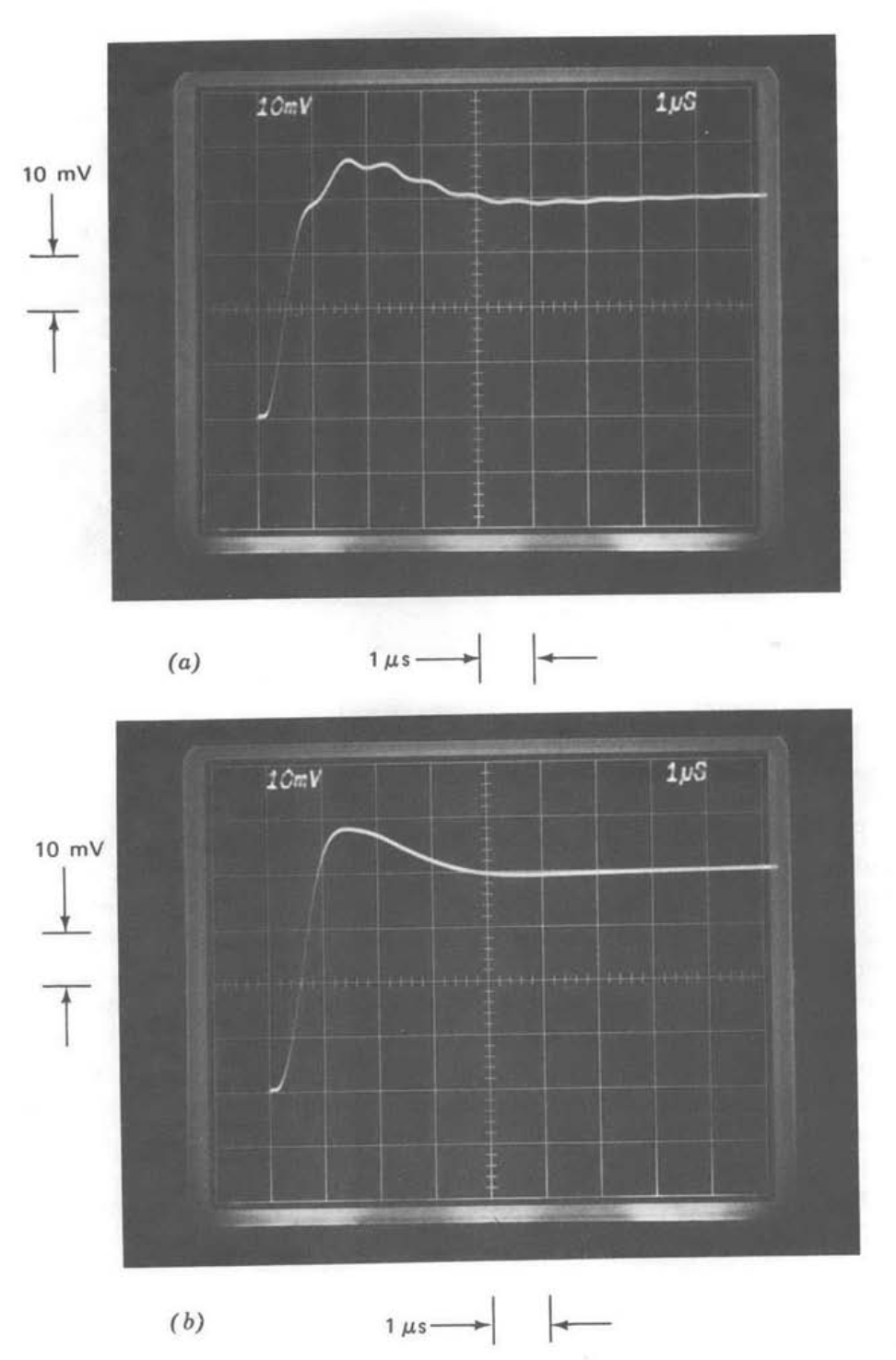
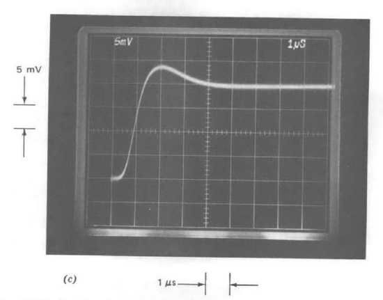
Figure 13.27 Step response of unity-gain inverter loaded with \(0.1\ \mu F\) capacitor and compensated with a zero. (Input-step amplitude is \(40\ mV\) for parts \(a\) and \(b\), \(2\ mV\) for part \(c\).) (\(a\)) With series resistor-capacitor compensation. (\(b\)) With compensating network of Figure 13.29. (\(c\)) Smaller amplitude input signal.
The step response of the test amplifier connected this way is shown in Figure 13.27\(a\). Although the basic structure of the transient response is far superior to that shown in Figure 13.25\(b\), there is a small-amplitude high-frequency ringing superimposed on the main transient. This component, at a frequency well above the major-loop crossover frequency, reflects potential minor-loop instability.
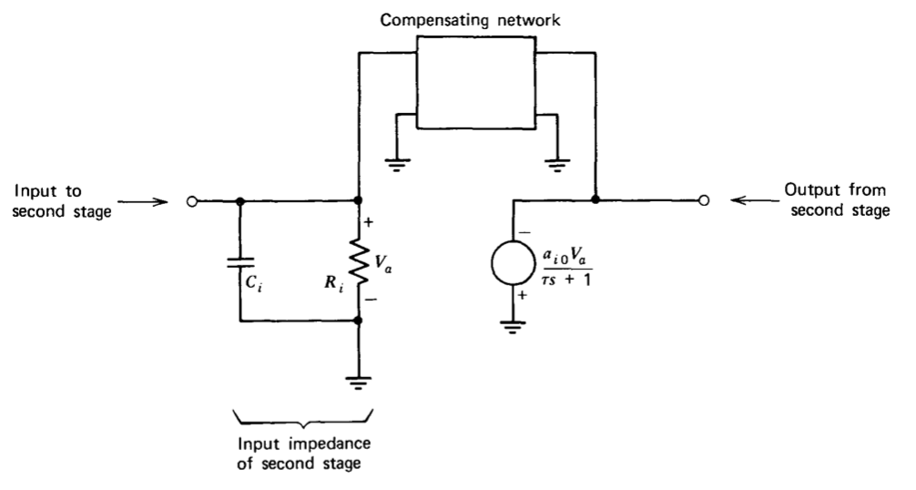
Figure 13.28 Model for second stage of a two-stage amplifier.
Figure 13.28 illustrates the mechanism responsible for the instability. This diagram combines an idealized model for the second stage of a two-stage amplifier with a compensating network. (The discussion of Section 9.2.3 justifies this general model for a high-gain stage.) When the crossover frequency of the loop formed by the compensating network is much higher than \(1/R_iC_i\), the second stage input looks capacitive at crossover. If the compensating-network transfer admittance is capacitive in the vicinity of crossover, the phase margin of the inner loop approaches \(90^{\circ}\). Alternatively, if the compensating network is resistive, the input capacitance introduces a second pole into the inner-loop transmission and the phase margin of this loop drops.
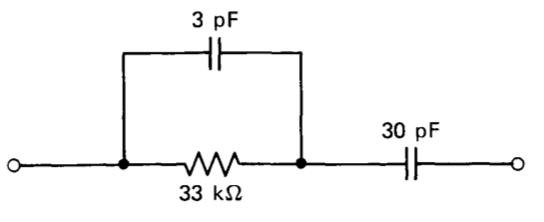
Figure 13.29 Compensating network used to obtain transients shown in Figs. 13.27\(b\) and 13. 27\(c\).
The solution is to add a small capacitor to the compensating network as indicated in Figure 13.29. The additional element insures that the network transfer admittance is capacitive at the minor-loop crossover frequency, thus improving stability. The approximate loop transmission of the major loop is changed from that given in Equation \(\ref{eq13.3.28}\) to
\[L(s) \simeq - \dfrac{7.7 \times 10^6 (10^{-6} s + 1)}{s (6.5 \times 10^{-6} s + 1)(10^{-7} s + 1)}\lable{eq13.3.29} \nonumber \]
The effect on the major loop is to introduce a pole at a frequency approximately a factor of 7 above crossover, thereby reducing phase margin by \(8^{\circ}\).
The step response shown in Figure 13.27\(b\) results with this modification. An interesting feature of this transient is that it also has a tail with a duration that seems inconsistent with the speed of the initial rise. While there is a zero included in the closed-loop transfer function of this connection since the zero in Equation \(\ref{eq13.3.29}\) occurs in the forward path, the zero is close to the crossover frequency of the major loop. Consequently, any tail that resulted from a doublet formed by a closed-loop pole combining with this zero would have a decay time consistent with the crossover frequency of the major loop. In fact, the duration of the tail evident in Figure 13.27\(b\) is reasonable in view of the \(1.4 \times 10^6\) radian-per-second crossover frequency of the major loop. The inconsistency stems from an initial rise that is too fast.
The key to explaining this phenomenon is to note that the output- signal slope reaches a maximum value of approximately \(6 \times 10^4\) volts per second, implying a \(6-mA\) charging current into the \(0.1-\mu F\) capacitor. This current level is substantially above the quiescent current of the output stage of the LM301A, and results in a lowered output resistance from the active emitter follower during the rapid transition. Consequently, the pole associated with capacitive loading moves toward higher frequencies during the initial high-current transient, and the speed of response of the system im proves in this portion.
Figure 13.27\(c\) verifies this reasoning by illustrating the response of the capacitively loaded follower to a \(2-mV\) input signal step. A gain-of-10 amplifier (realized with another appropriately compensated LM301A) amplified the output signal to permit display at the 5 mV-per-division level indicated in the photograph. While this transient is considerably more noisy (reflecting the lower-amplitude signals), the relative speed of various portions of the transient is more nearly that expected of a linear system.
The fractional change in output resistance with output current level is probably less than 25% for this amplifier because the dominant component of output resistance is the value at the high-resistance node divided by the current gain of the buffer amplifier. Consequently, the differences between Figs. 13.27\(b\) and 13.27\(c\) are minor. It should also be noted that the esti mated value for \(R_o\) (Equation \(\ref{eq13.3.24}\)) is probably slightly low because of this effect.
Many applications, such as sample-and-hold circuits or voltage regulators, apply capacitive loading to an operational amplifier. Other connections, such as a differentiator, add a pole to the loop transmission because of the transfer function of the feedback network. The method of adding a zero to single-pole compensation can improve performance substantially in these types of applications.
The comparison between Figs. 13.25\(b\) and 13.27\(b\) shows how changing from \(30-pF\) compensation to compensation that includes a zero can greatly improve stability and can reduce settling time by more than a factor of 10 for a capacitively loaded voltage follower.
It should be emphasized that this type of compensation is not suggested for general-purpose use, since the compensating-network element values must be carefully chosen as a function of loop-parameter values for accept able stability. If, for example, the pole that introduced the need for this type of compensation is eliminated or moved to a higher frequency, the cross over frequency increases and instability may result.
Slow-Rolloff Compensation
The discussion of the last section showed how compensation can be designed to introduce a zero into the compensated open-loop transfer function of an operational amplifier. The zero can be used to offset the effects of a pole associated with other elements in the loop. Since the zero location is selected as a function of other loop parameters, this type of compensation is effectively specifically tailored for one fixed feedback network and load.
There are applications where the transfer functions of certain elements in an operational-amplifier loop vary as a function of operating conditions or as the components surrounding the amplifier change. The change in amplifier open-loop output resistance described in connection with Figs. 13.27\(b\) and 13.27\(c\) is one example of this type of parameter variation.
Operational amplifiers that are used (often with the addition of high-current output stages) to supply regulated voltages are another example. The total capacitance connected to the output of a supply is often dominated by the decoupling capacitors included with the circuits it powers. The out put resistance of the power stage may also be dependent on load current, and these two effects can combine to produce a major uncertainty in the location of the pole associated with capacitive loading. One approach to stabilizing this type of regulator was described in Section 5.2.2.
A third example of a variable-parameter loop involves the use of an operational amplifier, an incandescent lamp, and a photoresistor in a feedback loop intended to control the intensity of the lamp. In this case, the dynamics of both the lamp and the photoresistor as well as the low-fre quency "gain" of the combination depend on light level.
The stabilization of variable-parameter systems is often difficult and compromises, particularly with respect to settling time and desensitivity, are frequently necessary. This section describes one approach to the stabilization of such systems and indicates the effect of the necessary compromises on performance.
Consider a variable-parameter system that has a loop transmission
\[L(s) = -a(s) \left (\dfrac{k}{\tau s + 1} \right ) \label{eq13.3.30} \]
where \(k\) and \(\tau\) represent the uncertain values associated with elements external to the operational amplifier. It is assumed that these parameters can have any positive values. If the amplifier open-loop transfer function is selected such that
\[a(s) = \dfrac{K'}{\sqrt{s}} \label{eq13.3.31} \]
the phase margin of Equation \(\ref{eq13.3.30}\) will be at least \(45^{\circ}\) for any values of \(k\) and \(\tau\), since the phase shift of the function \(1/\sqrt{s}\) is \(-45^{\circ}\) at all frequencies.
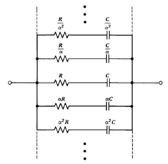
Figure 13.30 Network used to approximate an admittance proportional to \(\sqrt{s}\).
In order to obtain the open-loop transfer function indicated by Equation \(\ref{eq13.3.31}\) from a two-stage amplifier, it is necessary to use a network that has a short-circuit transfer admittance proportional to \(\sqrt{s}\). While the required admittance cannot be realized with a lumped, finite network, it can be approximated by the ladder structure shown in Figure 13.30. The driving-point admittance of this network (which is, of course, equal to its short-circuit transfer admittance) is
\[Y_c (s) = + \cdots + \dfrac{(C/\alpha^2)s}{(RC/\alpha^4)s + 1} + \dfrac{(C/\alpha )s}{(RC/\alpha^2)s + 1} + \dfrac{Cs}{RCs + 1} + \dfrac{\alpha Cs}{\alpha^2 RCs + 1} + \dfrac{\alpha^2 Cs}{\alpha^4 RCs + 1} + \cdots + \label{eq13.3.32} \]
The poles of Equation \(\ref{eq13.3.32}\) are located at
\[\begin{array} {rcl} {} & \cdot & {} \\ {} & \cdot & {} \\ {} & \cdot & {} \\ {p_{n + 2}} & = & {-\dfrac{\alpha^4}{RC}} \\ {p_{n + 1}} & = & {-\dfrac{\alpha^2}{RC}} \\ {p_n} & = & {-\dfrac{1}{RC}} \\ {p_{n - 1}} & = & {-\dfrac{1}{\alpha^2 RC}} \\ {p_{n - 2}} & = & {-\dfrac{1}{\alpha^4 RC}} \\ {} & \cdot & {} \\ {} & \cdot & {} \\ {} & \cdot & {} \end{array} \nonumber \]
while its zeros are located at
\[\begin{array} {rcl} {} & \cdot & {} \\ {} & \cdot & {} \\ {} & \cdot & {} \\ {z_{n + 2}} & = & {-\dfrac{\alpha^3}{RC}} \\ {z_{n + 1}} & = & {-\dfrac{\alpha}{RC}} \\ {z_n} & = & {-\dfrac{1}{\alpha RC}} \\ {z_{n - 1}} & = & {-\dfrac{1}{\alpha^3 RC}} \\ {z_{n - 2}} & = & {-\dfrac{1}{\alpha^5 RC}} \\ {} & \cdot & {} \\ {} & \cdot & {} \\ {} & \cdot & {} \end{array} \nonumber \]
This admittance function has poles and zeros that alternate along the negative real axis, with the ratio of the locations of any two adjacent singularities a constant equal to \(\alpha\). On the average, the magnitude of this function will increase proportionally to the square root of frequency since on an asymptotic log-magnitude versus log-frequency plot it alternates equal-duration regions with slopes of zero and one.
If this network is used to compensate a two-stage amplifier, the amplifier open-loop transfer function
\[a(s) \simeq \dfrac{K}{Y_c (s)}\label{eq13.3.35} \]
will approximate the relationship given in Equation \(\ref{eq13.3.31}\). If the magnitude of uncompensated amplifier open-loop transfer function is adequately high, the range of frequencies over which the approximation is valid can be made arbitrarily wide by using a sufficiently large number of sections in the ladder network. Note that it is also possible to make the compensated transfer function be proportional to \(1/s^r\), where \(r\) is between zero and one, by appropriate selection of relative pole-zero spacing in the compensating network.
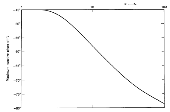
Figure 13.31 Maximum negative phase shift as a function of \(\alpha\) for \(1/\sqrt{s}\) compensation.
Since the usual objective of this type of compensation is to maintain satisfactory phase margin in systems with uncertain parameter values, guidelines for selecting the frequency ratio between adjacent singularities a are best determined by noting how the phase of the actual transfer function is influenced by this quantity. If the poles and zeros are closely spaced, the phase shift of the compensated open-loop transfer function will be approximately \(- 45^{\circ}\) over the effective frequency range of the network. As a is increased, the magnitude of the phase ripple with frequency, which is symmetrical with respect to \(- 45^{\circ}\), increases. The maximum negative phase shift of \(a(j\omega)\) (see Equations \(\ref{eq13.3.32}\) and \(\ref{eq13.3.35}\)) is plotted as a function of a in Figure 13.31.
This plot shows that reasonably large values of a can be used without the maximum negative phase shift becoming too large. If, for example, a spacing between adjacent singularities of a factor of 10 in frequency is used, the maximum negative phase shift is \(-58^{\circ}\). Since the phase ripple is symmetrical with respect to \(-45^{\circ}\), the phase shift varies from \(-32^{\circ}\) to \(-58^{\circ}\) as a function of frequency for this value of \(\alpha\). If an amplifier compensated using a network with \(\alpha = 10\) is combined in a loop with an element that produces an additional \(-90^{\circ}\) of phase shift at crossover, the system phase margin will vary from \(58^{\circ}\) to \(32^{\circ}\).
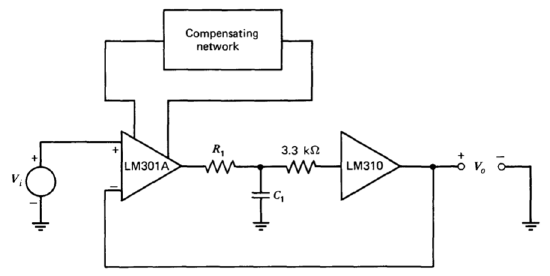
Figure 13.32 Circuit used to evaluate slow-rolloff compensation.
The performance of a \(1/\sqrt{s}\) system is compared with that of alternatively compensated systems using the-,connection shown in Figure 13.32. Providing that the open-loop output resistance of the operational amplifier is much lower than \(R_1\), the \(R_1-C_1\) network adds a pole with a well-determined location to the loop transmission of the system. The LM310 unity-gain follower is used to avoid loading the network. The \(3.3-k\Omega\) resistor included in series with the LM310 input is recommended by the manufacturer to improve the stability of this circuit. The bandwidth of this follower is high enough to have a negligible effect on loop dynamics.
The circuit shown in Figure 13.32 has a forward-path transfer function equal to \(a(s)/(RCs + 1)\) and a feedback transfer function of one.
Three different types of compensation were evaluated with this connection. One type was single-pole compensation using a \(220-pF\) capacitor. The approximate open-loop transfer function of the LM301A is
\[a(s) \simeq \dfrac{10^6}{s}\label{eq13.3.36} \]
with this compensation. The corresponding loop transmission is
\[L(s) = -\dfrac{10^6}{s (R_1 C_1 s + 1)} \nonumber \]
The closed-loop transfer function is
\[\dfrac{V_o (s)}{V_i (s)} = A(s) = \dfrac{1}{10^{-6} R_1 C_1 s^2 + 10^{-6} s + 1}\label{eq13.3.38} \]
Second-order parameters for Equation \(\ref{eq13.3.38}\) are
\[\omega_n = \dfrac{10^3}{\sqrt{R_1 C_1}} \ \ \text{ and } \ \ \zeta = \dfrac{5 \times 10^{-4}}{\sqrt{R_1 C_1}} \nonumber \]
As expected, increasing the \(R_1-C_1\) time constant lowers both the natural frequency and the damping ratio of the system.
The second compensating network was an 11 "rung" ladder network of the type shown in Figure 13.30. The sequence of resistor-capacitor values used for the rungs was \(330\ \Omega-10\ pF\), \(1\ k\Omega-33\ pF\), \(3.3\ k\Omega-100\ pF \cdots 10\Omega-0.33\ \mu F, 33\ M\Omega - 1\ \mu F\).
This network combines with operational-amplifier parameters to yield an approximate open-loop transfer function
\[a'(s) \simeq \dfrac{10^3}{\sqrt{s}}\label{eq13.3.39} \]
over a frequency range that extends from below 0.1 radian per second to above \(10^6\) radians per second. The value of \(\alpha\) for the approximation is \(-\sqrt{10}\). The curve of Figure 13.31 shows that the maximum negative phase shift of the open-loop transfer function at intermediate frequencies should be \(-46.5^{\circ}\), corresponding to a peak-to-peak phase ripple of \(3^{\circ}\).
The approximate loop transmission that results with this compensation is
\[L' (s) = -\dfrac{10^3}{\sqrt{s} (R_1 C_1 s + 1)} \nonumber \]
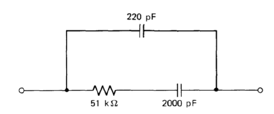
Figure 13.33 Slow-rolloff network.
The third compensation used the two-rung slow-rolloff network shown in Figure 13.33. The resultant amplifier open-loop transfer function is
\[a'' (s) \simeq \dfrac{10^5 (10^{-4} s + 1)}{s (10^{-5} s + 1)}\label{eq13.3.41} \]
This transfer function is a very crude approximation to a \(1/\sqrt{s}\) rolloff that combines a basic \(1/s\) rolloff with a decade-wide zero-slope region realized by placing a zero two decades and a pole one decade below the unity-gain frequency. Alternatively, the open-loop transfer function can be viewed as the result of adding a lead network located well below the unity-gain frequency to a single-pole transfer function.
The loop transmission in this case is
\[L'' (s) = -\dfrac{10^5 (10^{-4} s + 1)}{s(10^{-5} s + 1)(R_1 C_1 s + 1)}\label{eq13.3.42} \]
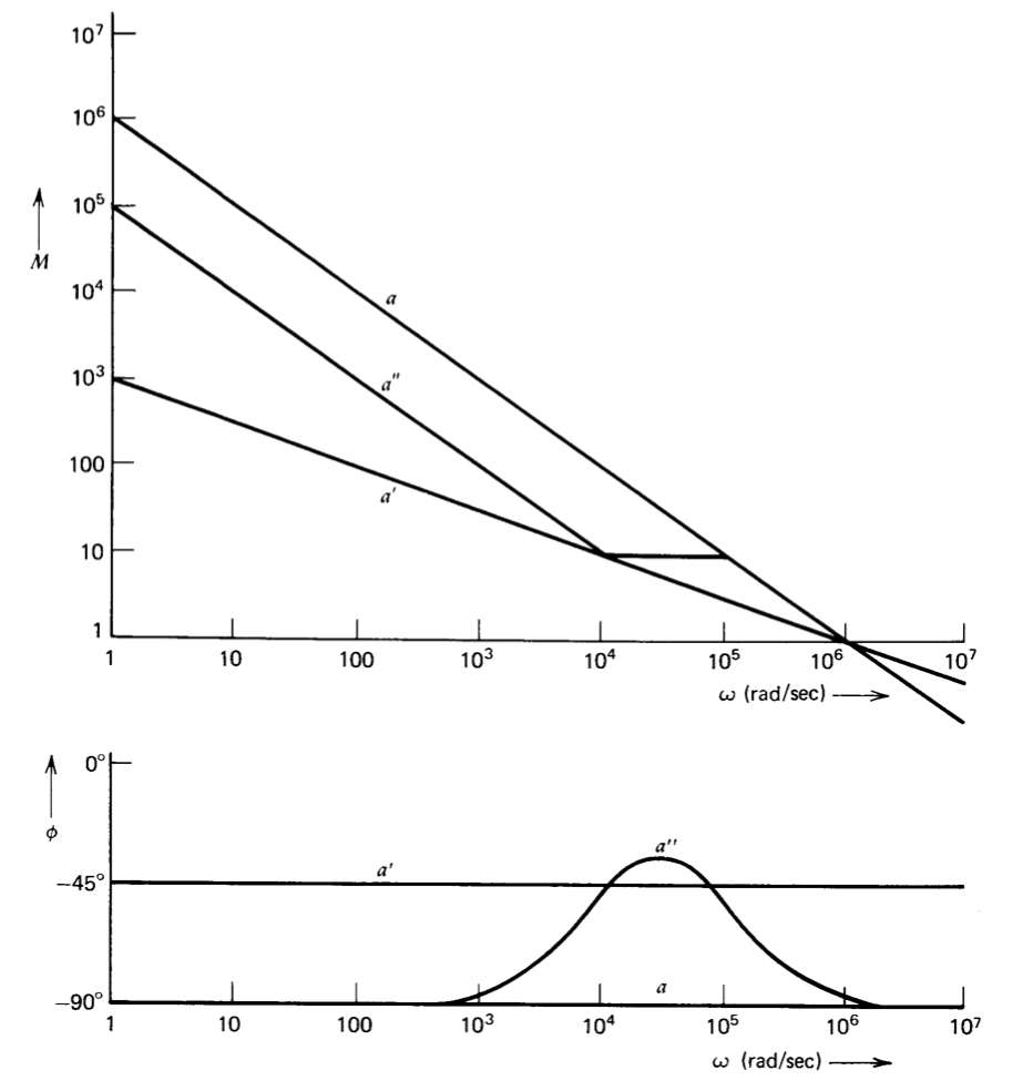
Figure 13.34 Comparison of approximate open-loop transfer functions for three types of compensation.
Bode plots for the three compensated open-loop transfer functions of Equations \(\ref{eq13.3.36}\), \(\ref{eq13.3.39}\), and \(\ref{eq13.3.41}\) are shown in Figure 13.34. Note that parameters are selected so that unity-gain frequencies are identical for the three transfer functions.
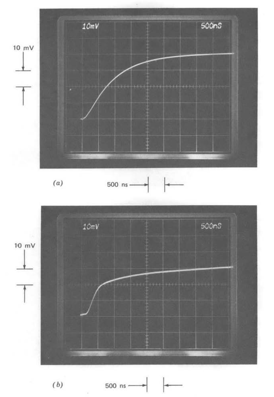
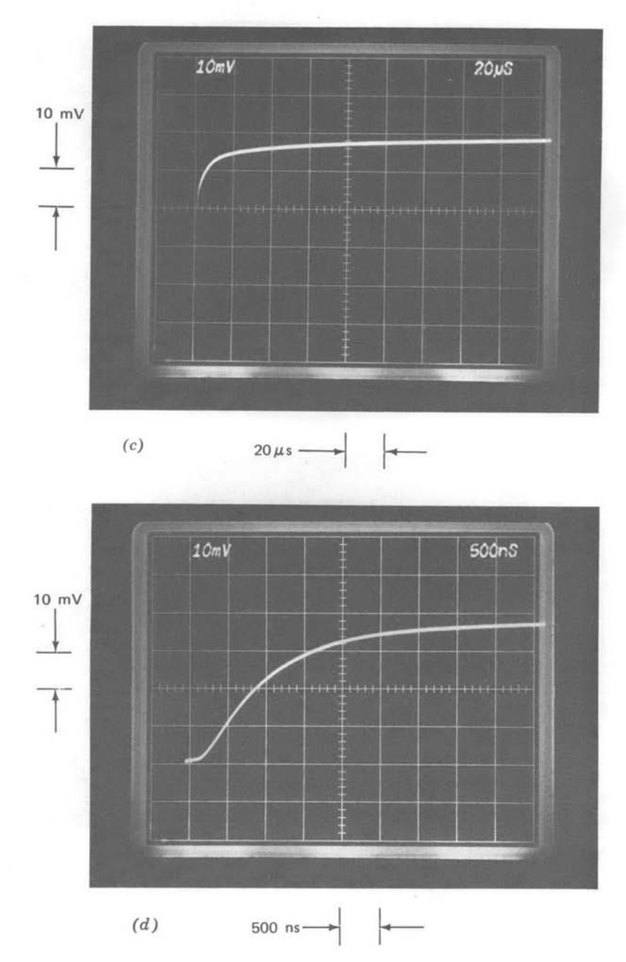
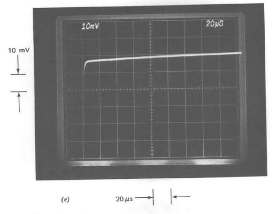
Figure 13.35 Comparison of step responses as a function of compensation with \(R_1C_1 = 0\). (Input-step amplitude is \(40\ mV\).) (\(a\)) One-pole compensation. (\(b\)) \(1/\sqrt{s}\) compensation. (\(c\)) Repeat of part \(b\) with slower sweep speed. (\(d\)) Slow-rolloff compensation. (\(e\)) Repeat of part \(d\) with slower sweep speed.
The step responses for the test system with \(R_1C_1 = 0\) are compared for the three types of compensation in Figure 13.35. Part a shows the step response for one-pole compensation. The expected exponential response with a \(1-\mu s\) 0 to 63 % rise time is evident.
Part b shows the response with the \(1/\sqrt{s}\) compensation. An interesting feature of this response is that while it actually starts out faster than that of the previous system with the same crossover frequency (compare, for example, the times required to reach 25% of final value), it settles much more slowly. Note that the transient shown in part \(b\) has only reached 75% of final value after \(4.5\ \mu s\) (the input-step amplitude is 40 mV for both parts \(a\) and \(b\)), while the system using one-pole compensation has settled to within 2% of final value by this time. Part \(c\) is a repeat of part \(b\) with a slower sweep speed. Note that even after \(180\ \mu s\), the transient has reached only 95% of final value. This type of very slow creep toward final value is characteristic of many types of distributed systems. Long transmission lines, for example, often exhibit step responses similar in form to that illustrated.
Parts \(d\) and \(e\) of Figure 13.35 show the response for the system using slow-rolloff compensation at two different time scales. The transient consists of a \(1-\mu s\) time constant exponential rise to 90% of final value, followed by a 100-us time constant rise to final value. The reader should use Equation \(\ref{eq13.3.42}\) to convince himself that the long tail is anticipated in view of the location of the closed-loop pole-zero doublet that results in this case. Note that even with this tail, settling to a small fraction of final value is substantially shorter than for the \(1/\sqrt{s}\) system.
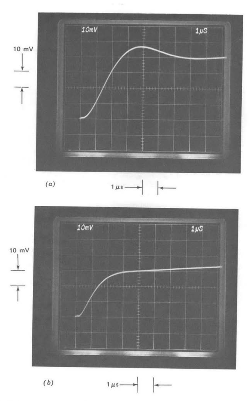
Figure 13.36 Comparison of step responses as a function of compensation for \(R_1 C_1 = 1\ \mu s\). (Input-step amplitude is \(40\ mV\).) (\(a\)) One-pole compensation. (\(b\)) \(1/\sqrt{s}\) compensation. (\(c\)) Slow-rolloff compensation.
Figure 13.36 indicates responses for \(R_1 C_1 = 1\ \mu s\) for the three different types of compensation. This \(R_1-C_1\) product adds a pole slightly above the resultant crossover frequency of the loop for all of the compensations. The phase margin of the system with one pole compensation is about \(50^{\circ}\), with the resulting moderate damping shown in part \(a\). The phase margin for \(1/\sqrt{s}\) compensation exceeds \(90^{\circ}\) in this case, and the main effect of the extra pole is to make the initial portion of the response (see part \(b\)) look somewhat more exponential. The very slow tail is not altered substantially. The step response of the system with slow-rolloff compensation (Figure 13.36\(c\)) has slightly less peak overshoot (measured from the final value shown in the figure) than does the system shown in part \(a\). The difference reflects the \(5^{\circ}\) phase-margin advantage of the slow-rolloff system. The tail is un altered by the additional pole.
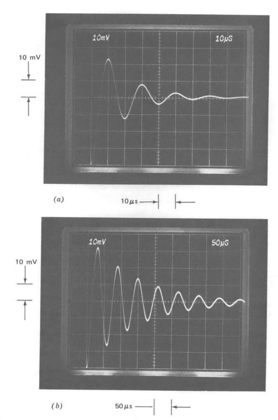
Figure 13.37 Step response of system with one-pole compensation as a function of \(R_1 C_1\). (Input-step amplitude is \(40\ mV\).) (\(a\)) \(R_1 C_1 = 10\ \mu s\). (\(b\)) \(R_1 C_1 = 100 \ \mu s\). (\(c\)) \(R_1 C_1 = 1\ ms\). (\(d\)) \(R_1 C_1 = 10\ ms\). (\(e\)) \(R_1 C_1 = 100\ ms\). (\(f\)) \(R_1 C_1 = 100\ ms\) with polystyrene capacitor.
The experimentally measured step response of the system with one-pole compensation is shown in Figure 13.37 for a number of values of the \(R_1-C_1\) time constant. The deterioration of stability and settling time that results as \(R_1 C_1\) is increased is clearly evident in this sequence. The value for natural frequency predicted by Equation \(\ref{eq13.3.38}\) can be verified to within experimental tolerances. However, the actual system is actually somewhat better damped than the analysis indicates, particularly in the relatively lower-damped cases. The unit-step response for a second-order system is
\[v_o (t) = \left [1 - \dfrac{1}{\sqrt{1 - \zeta^2}} e^{-\zeta \omega_n t} \sin \left ( \sqrt{1 - \zeta^2} \omega_n t + \Phi \right ) \right ] \nonumber \]
where
\[\Phi = \tan^{-1} \left [\dfrac{1 - \zeta^2}{\zeta} \right ] \nonumber \]
This relationship shows that the exponential time constant of the envelope of the transient should have a value of \(1/\zeta \omega_n\), or, from Equation \(\ref{eq13.3.38}\), \(2R_1C_1\). Thus, for example, the transient illustrated in Figure 13.37\(e\), which has analytically determined values of \(\omega_n = 3.1 \times 10^3\) radians per second and \(\zeta = 1.6 \times 10^{-3}\), should have a decay time approximately five times longer than that actually measured.
The reason for this discrepancy is as follows. An extension of the curves shown in Figure 4.26 estimates that a damping ratio of \(1.6 \times 10^{-3}\) corresponds to a phase margin of \(0.184^{\circ}\). Accordingly, very small changes in the angle of the loop transmission at the crossover frequency can change damping ratio by a substantial factor.
There are at least three effects, which (in apparent violation of Murphy's laws) combine to improve phase margin in the actual system. First, the compensated amplifier open-loop pole is not actually at the origin, and thus contributes less than \(90^{\circ}\) of negative phase shift to the loop transmission at crossover. Second, any series resistance associated with the connections made to the capacitor adds a zero to the loop transmission that contributes positive phase shift at crossover. Third, the losses associated with dielectric absorption or dissipation factor of the capacitor also improve the phase margin of the system.
The importance of the third effect can be seen by comparing parts \(e\) and \(f\) of Figure 13.37. For part e(and all preceding photographs) a ceramic capacitor was used. The transient indicated in part \(f\), with a decay time approximately three times that of part \(e\) and within 60%. of the analytically predicted value, results when a low-loss polystyrene capacitor is used in place of the ceramic unit. This comparison demonstrates the need to use low-loss capacitors in lightly damped systems such as oscillators.
It should also be noted that, in addition to very low damping, this type of connection can lead to inordinately high signal levels with the possibility of saturation at certain points inside the loop. Since the frequency of the ringing at the system output is higher than the cutoff frequency of the \(R_1-C_1\) low-pass network, the signal out of the LM301A will be larger than the system output signal during the oscillatory period. In fact, the peak signal level at the output of the LM301A exceeded 20 volts peak-to-peak during the transients shown in Figs. 13.37\(e\) and 13.37\(f\). Longer \(R_1-C_1\) time constants would have resulted in saturation with the \(40-mV\) step input.
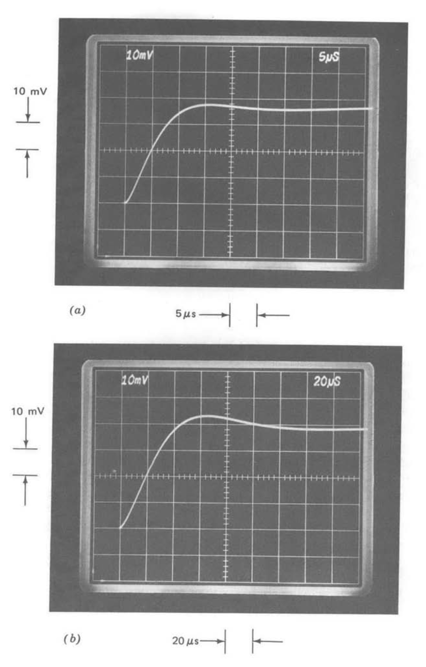
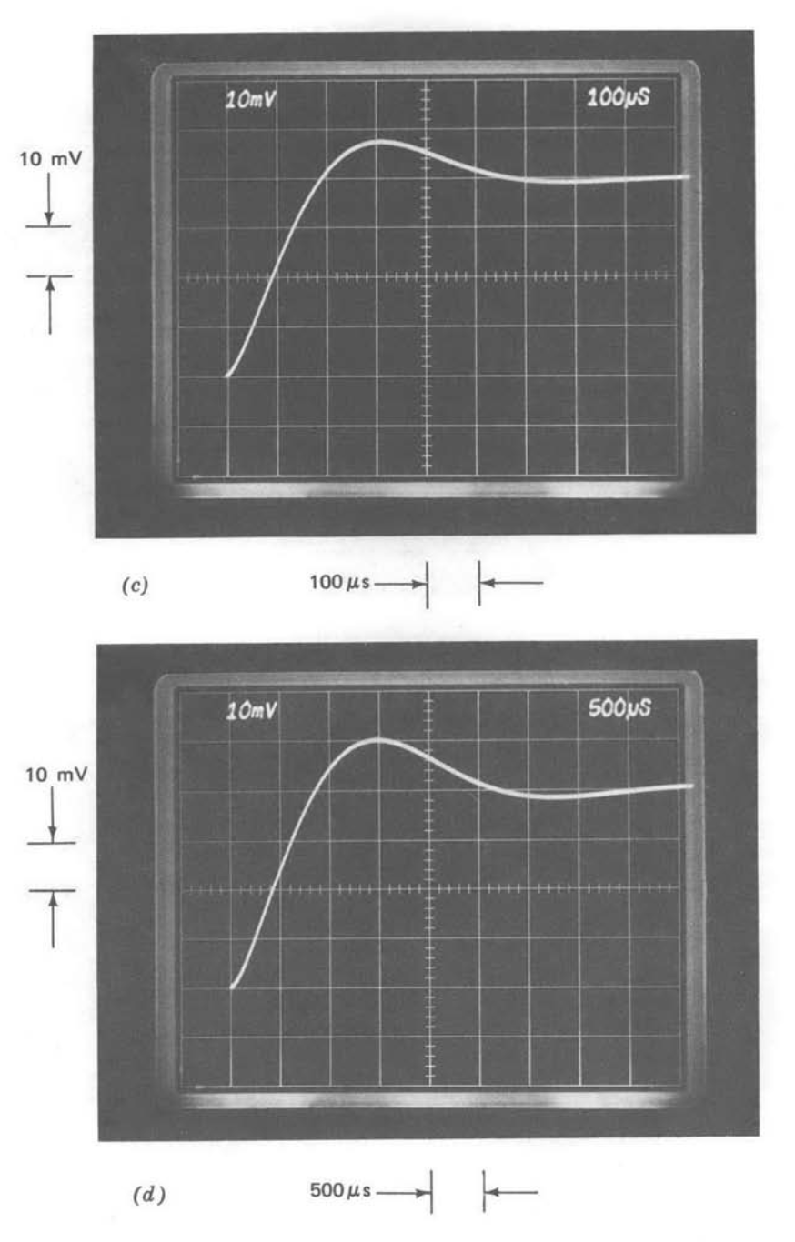
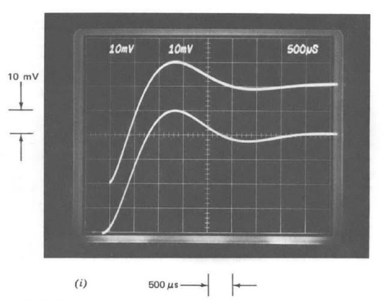
Figure 13.38 Step response of system with \(1/\sqrt{s}\) compensation as a function of \(R_1 C_1\). (Input-step amplitude is \(40 \ mV\).) (\(a\)) \(R_1 C_1 = 10\ \mu s\). (\(b\)) \(R_1 C_1 = 100\ \mu s\). (\(c\)) \(R_1 C_1 = 1\ ms\). (\(d\)) \(R_1 C_1 = 10\ ms\). (\(e\)) \(R_1 C_1 = 100\ ms\). (\(f\)) \(R_1 C_1 = 1\text{ second}\). (\(g\)) \(R_1 C_1 = 10\text{ seconds}\). (\(h\)) \(R_1 C_1 = 100\text{ seconds}\). (\(i\)) Comparison of part \(d\) with second-order system.
Figure 13.38 shows the responses of the system compensated with a \(1/\sqrt{s}\) amplifier rolloff as a function of the \(R_1-C_1\) product. Several analytically predictable features of this system are demonstrated by these responses. Since the magnitude of the loop transmission falls as \(1/\omega^{3/2}\) at frequencies above the pole of the \(R_1-C_1\) network and as \(1/\omega^{1/2}\) below the pole location, the loop crossover frequency decreases as \(1/R_1 C_1^{3/2}\). A factor of 10 increase in the \(R_1-C_1\) product lowers crossover by a factor of \(10^{2/3} = 4.64\), while a three-decade change in this product changes crossover by two decades. Comparing, for example, parts \(c\) and \(f\) or \(d\) and \(g\) of Figure 13.38 shows that while the general shapes of these responses are similar, the speeds differ by a factor of 100, reflecting the change in crossover frequency that occurs for a factor of 1000 change in the \(R_1-C_1\) product. Part \(h\) is somewhat faster than predicted by the above relation ship because, with an \(R_1-C_1\) value of 100 seconds, the corresponding pole lies at frequencies below the \(1/\sqrt{s}\) region of the compensation. (Recall that the longest time constant in the compensating network is 33 seconds.) The \(1/\sqrt{s}\) rolloff could be extended to lower frequencies by using more sections in the network, but very long time constants would be required. The amplifier d-c gain of approximately \(10^5\) would permit a \(1/\sqrt{s}\) rolloff from \(10^{-4}\) radian per second to unity gain at \(10^6\) radians per second.
The crossover frequencies for parts \(a, b\), and \(c\) are located at factors of approximately 2.16, 4.64, and 10, respectively, above the break frequency of the \(R_1-C_1\) network. Accordingly, the pole associated with the \(R_1-C_1\) net work produces somewhat less than \(- 90^{\circ}\) of phase shift in these cases, with the result that the phase margin is above \(45^{\circ}\). This effect is negligible in part \(d\) through \(h\), and the slight differences in damping evident in these transients arise because of the phase ripple of the compensating network. The actual ripple is probably larger than the \(3^{\circ}\) peak-to-peak value predicted in Figure 13.31 as a consequence of component tolerances.
The transient shown in Figure 13.38\(d\) results from a phase margin of ap proximately \(45^{\circ}\) and a crossover frequency of \(2.16 \times 10^3\) radians per second. The curves of Figure 4.26 indicate that the appropriate approximating second-order system in this case is one with \(\zeta = 0.42\) and \(\omega_n = 2.5 \times 10^3\) radians per second. The two responses shown in Figure 13.38\(i\) compare the transient shown in part \(d\) with a second-order response using the parameters developed with the aid of Figure 4.26. The reader is invited to guess which transient is which.
The remarkable similarity of these two transients is a further demonstration of the validity of approximating the response of a complex system with a far simpler transient. Note that while the actual system includes 12 capacitors (exclusive of device capacitances internal to the operational amplifier), its transient response can be accurately approximated by that of a second-order system.
The transient responses shown in Figure 13.38 and Figure 13.36\(b\) illustrate how \(1/\sqrt{s}\) compensation can maintain remarkably constant relative stability as a system pole location is varied over eight decades of frequency. Actually, even lower values for the \(R_1-C_1\) break frequencies(While \(R_1-C_1\) time constants in excess of about 10 seconds cause some deviation from \(1/\sqrt{s}\) characteristics in the vicinity of the \(R_1-C_1\) pole, the phase margin is determined by the network characteristics at the crossover frequency. The system phase margin will remain approximately \(45^{\circ}\) for \(R_1-C_1\) time constants as large as \(10^4\) seconds.) yield comparable results, although difficulties associated with obtaining the very long time constants required and photographing the resulting slow transients prevented including additional responses.
Since this type of compensation eliminates the relatively high-frequency oscillations of the output signal, the signal levels at the output of the LM301A are considerably smaller than when one-pole compensation is used.
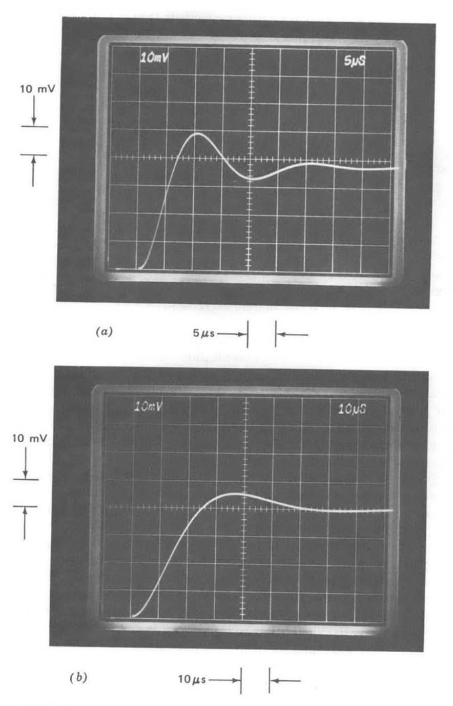
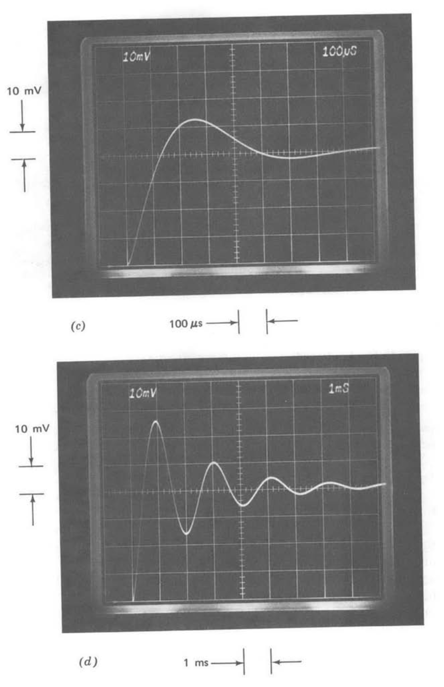
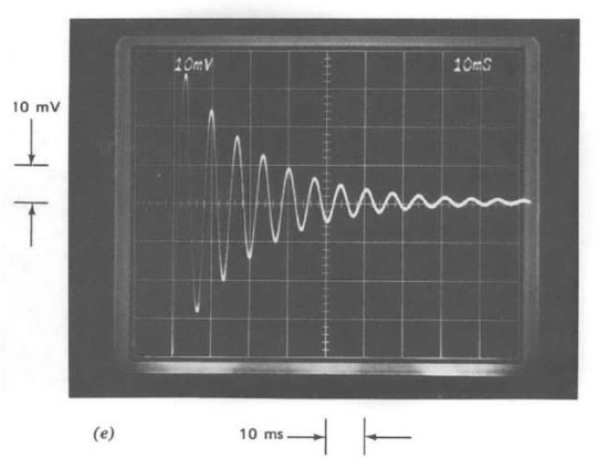
Figure 13.39 Step response for system with slow-rolloff compensation as a function of \(R_1C_1\). (Input-step amplitude = \(40\ mV\).) (\(a\)) \(R_1 C_1 = 10\ \mu s\). (\(b\)). \(R_1 C_1 = 100\ \mu s\). (\(c\)) \(R_1 C_1 = 1 \ ms\). (\(d\)) \(R_1 C_1 = 10\ ms\). (\(e\)) \(R_1 C_1 = 100\ ms\).
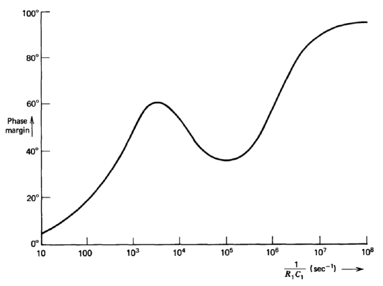
Figure 13.40 Phase margin as a function of \(1/R_1 C_1\) for \(L'' (s) = -[10^5 (10^{-4} s + 1)/s (10^{-5} s + 1)(R_1 C_1 s + 1)]\).
The step response of the system with slow-rolloff compensation is indicated in Figure 13.39 for values of \(R_1 C_1\) from \(10\ \mu s\) to \(100\ ms\). The important point illustrated in these photographs is that the response of the system remains moderately well damped for \(R_1-C_1\) products as large as \(1\ ms\), and that the damping is superior to that of the system using single-pole compensation for any \(R_1-C_1\) value shown. The reason is explained with the aid of Figure 13.40, which is a plot of phase margin as a function of \(1/R_1 C_1\) for this system. Note that the phase margin exceeds \(30^{\circ}\) for any value of \(R_1C_1\) less than approximately \(3\ ms\).
While the variation in phase margin with \(R_1C_1\) is larger for this system than for the system with \(1/\sqrt{s}\) compensation, this type of compensation can result in reasonable stability as the location of the variable pole changes from more than three decades below the unity-gain frequency of the amplifier upward. In exchange for the somewhat greater variation in phase margin as a function of the \(R_1-C_1\) time constant and a more limited range of this product for acceptable stability, the complexity of the amplifier compensating network is reduced from 22 to three components.
Simple slow rolloff networks typified by that described above provide useful compensation in many practical variable-parameter systems because the range of parameter variation is seldom as great as that used to illustrate the performance of the system with \(1/\sqrt{s}\) compensation. Furthermore, other effects may combine with slow-rolloff compensation to increase its effectiveness in actual systems. Consider the voltage regulator with an arbitrarily large capacitive load mentioned earlier as an example of a variable parameter system. The series resistance and dissipation characteristic of electrolytic capacitors add a zero to the pole associated with the capacitive load, and this zero can aid slow-rolloff compensation in stabilizing a regulator for a very wide range of load-capacitor values.
It is also evident that adding one or more rungs to the compensating network can increase the range of this type of compensation when required.
Feedforward Compensation
Feedforward compensation was described briefly in Section 8.2.2. This method, which differs in a fundamental way from minor-loop compensation, involves capacitively coupling the signal at the inverting input terminal of an operational amplifier to the input of the final voltage-gain stage. This final stage is assumed to provide an inversion. The objective is to eliminate the dynamics of all but the final stage from the amplifier open-loop transfer function in the vicinity of the unity-gain frequency.
This approach, which has been used since the days of vacuum-tube operational amplifiers, is not without its limitations. Since only signals at the inverting input terminal are coupled to the output stage, the feedforward amplifier has much lower bandwidth for signals applied to its noninverting input and generally cannot be effectively used in noninverting configurations.(There have been several attempts at designing amplifiers that use dual feed-forward paths to a differential output stage. One of the. difficulties with this approach arises from mismatches in the feedforward paths. A common-mode input results in an output signal because of such mismatches. The time required for the error to settle out is related to the dynamics of the bypassed amplifier, and thus very long duration tails result when these amplifiers are used differentially.)
Another difficulty is that the phase shift of a feedforward amplifier often approaches \(-180^{\circ}\) at frequencies well below its unity-gain frequency. Accordingly, large-signal performance may be poor because the amplifier is close to conditional stability. The excessive phase shift also makes feed- forward amplifiers relatively intolerant of capacitive loading.
Feedforward is normally most useful for three or more stage amplifiers, and results in relatively little performance improvement for many two-stage designs because the first stage of these amplifiers is often faster than the rest of the amplifier. The LM101A(R. C. Dobkin, Feedforward Compensation Speeds Op Amp, Linear Brief 2, National Semiconductor Corporation.) is an exception to this generality. Recall that the input stage of this amplifier includes lateral-PNP transistors. Because NPN transistors are used for voltage gain in the second stage, the first stage represents the bandwidth bottleneck for the entire amplifier.(The unity-gain output stage of this amplifier also uses lateral-PNP transistors. However, the buffer stage has approximately unity small-signal voltage gain even at frequencies where the common-emitter current gain of the lateral PNP's in this stage is zero. Thus these transistors do not have the dominant effect on amplifier bandwidth that the input transistors do.) Since the input to the second amplifier stage is available as a compensating terminal, feedforward that bypasses the narrow-bandwidth stage can be implemented by connecting a capacitor from the inverting input terminal of the amplifier to this compensation terminal.
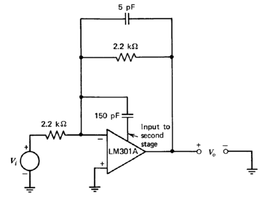
Figure 13.41 Unity-gain inverter with feedforward compensation.
The LM301A was connected as shown in Figure 13.41. Low-value resistors and the \(5-pF\) capacitor are used to reduce the effects of amplifier input capacitance on loop transmission. The \(150-pF\) feedforward capacitor is the value recommended by National Semiconductor Corporation, although other values may give better performance in some applications. This capacitor value can be selected to minimize the signal at the inverting input terminal (which is proportional to the error between actual and ideal output) if optimum performance is required.
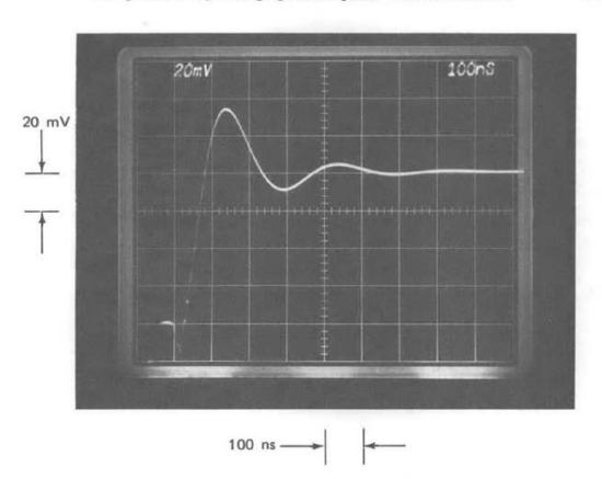
Figure 13.42 Step response of unity-gain inverter with feedforward compensation. (Input-step amplitude is \(-80\ mV\).)
The step response of this inverter is shown in Figure 13.42. There is substantial overshoot evident in the figure, as well as some "teeth" on the rising portion of the waveform that are probably at least partially related to high-speed grounding problems in the test set up. The 10 to 90% rise time of the circuit is approximately \(50\ ns\), or a factor of three faster than the fastest rise time obtained with minor-loop compensation (see Figure 13.13\(b\)).
Compensation to Improve Large-Signal Performance
The discussion in earlier parts of this chapter has focused on how compensation influences the linear-region performance of an operational amplifier. The compensation used in a particular connection also has a profound effect on the large-signal performance of the amplifier, particularly the slew rate or maximum time rate of change of output signal and how grace fully the amplifier recovers from overload.
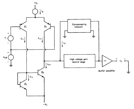
Figure 13.43 Operational-amplifier model.
The simplified two-stage amplifier representation shown in Figure 13.43 illustrates how compensation can determine the linear operating region of the amplifier. This model, which includes a current repeater, can be slightly modified to represent many available two-stage integrated-circuit operational amplifiers such as the LM101A. Elimination of the current repeater, which does not alter the essential features of the following argument, results in a topology adaptable to the discrete designs that do not include these transistors.
The key to understanding the performance of this amplifier is to recognize that, with a properly designed second stage, the input current required by this stage is negligible when it is in its linear operating region. Accordingly,
\[i_N = i_{C4} - i_{C2} \nonumber \]
This relationship, coupled with the fact that the incremental voltage change at the input of the second stage is also small under many operating conditions, is sufficient to determine the open-loop transfer function of the amplifier as a function of the compensating network.
Since the second stage normally operates at current levels large compared to those of the first stage, the limits of linear-region operation are usually determined by the first stage. Note that first-stage currents are related to the total quiescent bias current of this stage, \(I_B\), and the differential input voltage. For the topology shown, the relationship between the relative input-stage collector currents and input voltage becomes highly nonlinear when the differential input voltage v exceeds approximately \(kT/q\). At room temperature, for example, a \(+25-mV\) value for \(v_I\) raises the collector current of \(Q_2\) a factor of 1.46 above its quiescent level, while input voltages of \(60\ mV\) and \(120\ mV\) increase \(i_{C2}\) by factors of 1.82 and 1.98, respectively, above the quiescent value.
When a differential input-voltage level in excess of \(100\ mV\) is applied to the amplifier, the magnitude of the current \(i_{C4} - i_{C2}\) will have nearly its maximum value of \(I_B\). Regardless of how much larger the differential input signal to the amplifier becomes, the current from the input stage and, thus, the current iN, remains relatively constant.
Even if series emitter resistors are included (as they are in some amplifiers at the expense of drift referred to the input of the amplifier), or if more junctions are connected in the input-signal path as in the LM10A amplifier, the maximum magnitude of the current supplied by the first stage is bounded by its bias level. Since the value of iN cannot exceed the current supplied by the first stage (at least if the second stage remains linear), the output voltage can not have characteristics that cause \(i_N\) to exceed a fixed limit. If, for example, a capacitor with a value \(C_c\) is used for compensation,
\[i_N \simeq C_c v_O \nonumber \]
where the dot indicates time differentiation. Thus, for the values shown in Figure 13.43, the maximum magnitude of \(\dot{v}_O\) is
\[|\dot{v}_O|_{\max} = \dfrac{I_B}{C_c} \label{eq13.3.46} \]
One of the more restrictive design interrelationships for a two-stage amplifier is that with single-capacitor compensation and without emitter degeneration in the input stage, both the maximum time rate of change of output voltage and the unity-gain frequency of the amplifier are directly proportional to first-stage bias current. Hence increases in slew rate can only be obtained in conjunction with identical increases in unity-gain frequency. Since stability considerations generally bound the unity-gain frequency, the maximum slew rate is also bounded.
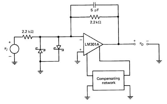
Figure 13.44 Inverter used to evaluate large-signal response.
The large-signal performance of the LM301A operational amplifier used in all previous tests is demonstrated using the connection shown in Figure 13.44. This connection is identical to the inverter used with feedforward compensation, except for the addition of Schottky diodes that function as
an input clamp. If clamping were not used, the voltage at the inverting in put of the amplifier would become approximately half the magnitude of a step input-voltage change immediately following the step because of direct resistive coupling. This type of transient would add currents to the output of the first stage because of signals fed through the collector-to-base junctions of the input transistors and because of transient changes in current-source levels. The Schottky diodes are used in preference to the usual silicon \(P-N\) junction diodes because they have superior dynamic characteristics and because their threshold voltage of approximately 0.3 volt is closer to the minimum value that guarantees complete input-stage current steering for the LM301A.
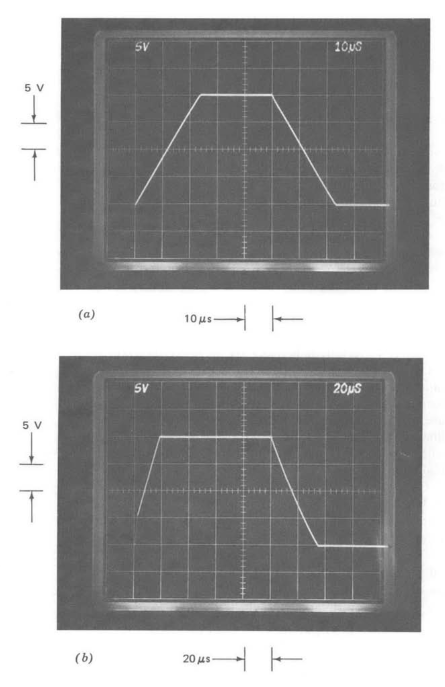
Figure 13.45 Large-signal response of LM301A with a \(30-pF\) compensating capacitor. (Input square-wave amplitude is 20 volts peak-to-peak.) (\(a\)) Unity-gain inverter. (\(b\)) Unity-gain voltage follower.
The square-wave response of the circuit of Figure 13.44 with a \(30-pF\) compensating capacitor is shown in Figure 13.45\(a\). The positive and negative slew rates are equal and have a magnitude of approximately 0.85 volt per microsecond. Note that there is no discernible overshoot as the amplifier output voltage reaches final value, indicating that the amplifier with this compensation recovers quickly and cleanly from the overload associated with a 20-volt step input signal.
The transient of Figure 13.45\(b\) is the response of a unity-gain voltage follower, compensated with a \(30-pF\) capacitor, to the same input. In this case, the positive transition has a step change followed by a slope of approximately 0.8 volt per microsecond, while the negative-transition slew rate is somewhat slower. The lack of symmetry reflects additional first-stage currents related to rapidly changing common-mode signals. Figure 13.43 indicates that a common-mode input applied to this type of amplifier forces voltage changes across the collector-to-base capacitances of the input transistors and the current source. The situation for the LM301A is somewhat worse than that depicted in Figure 13.43 because of the gain provided to bias current source variations by the lateral PNP's used in the input stage (see Section 10.4.1). The nonsymmetrical slewing that results when the amplifier is used differentially is the reason that the inverter connection was selected for the following demonstrations.
An earlier development showed that slew rate is related to input-stage bias current and compensating-capacitor size with single-pole compensation. Solving Equation \(\ref{eq13.3.46}\) for \(I_B\) using values associated with Figure 13.45\(a\) yields a bias current of 25.5 \(\mu A\), with half this current flowing through each side of the input-stage differential connection under quiescent conditions. The transconductance of the input-stage transistors, based on this estimated value of quiescent current, is approximately \(5 \times 10^{-4}\) mho.
Recall that the constant which relates the linear-region open-loop transfer function of the LM301A to the reciprocal of the compensating-network transfer admittance is one-half the transconductance of the input transis tors. The value for \(g_m/2\) of \(2.3 \times 10^{-4}\) mho determined in Equation \(\ref{eq13.3.9}\) from linear-region measurements is in excellent agreement with the estimate based on slew rate.
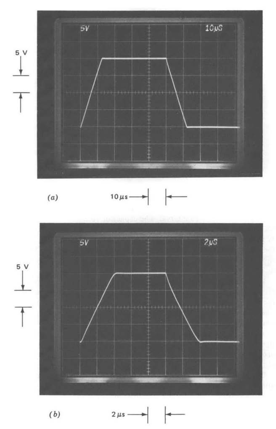
Figure 13.46 Slew rate as a function of compensating capacitor for unity-gain inverter. (Input square-wave amplitude is 20 volts peak-to-peak.) (\(a\)) \(C_c = 15\ pF\). (\(b\)) \(C_c = 5\ pF\) and input lag compensation.
Since slew rate with single-pole compensation is inversely related to compensating-capacitor size, one simple way to increase slew rate is to decrease this capacitor size. The transient shown in Figure 13.46\(a\) results with a \(15-pF\) compensating capacitor, a value that yields acceptable stability in the unity-gain inverter connection. As anticipated, the slew rate is twice that shown in Figure 13.45\(a\).
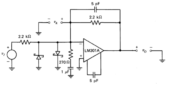
Figure 13.47 Unity-gain inverter with input lag compensation.
In order to maintain satisfactory stability with smaller values of compensating capacitor, it is necessary to lower the transmission of the elements surrounding the amplifier. The connection shown in Figure 13.47 uses input lag compensation to increase the attenuation from the output of the amplifier to its inverting input to approximately a factor of 10 at intermediate and high frequencies. It was shown in Section 13.3.2 that well-damped linear-region performance results with a \(4.5-pF\) compensating capacitor when the network surrounding the amplifier provides this degree of attenuation.
The response of Figure 13.46\(b\) results with a \(5-pF\) compensating capacitor and input lag compensation as shown in Figure 13.47. The slew rate increases to the value of 5 volts per microsecond predicted by Equation \(\ref{eq13.3.46}\) with this value for \(C_c\).
The large capacitor is used in the lag network to move the two-pole roll-off region that results from lag compensation well below crossover. This location improves recovery from the overload that results during the slewing period because large gain changes (in a describing-function sense) are required to reduce crossover to a value that results in low phase margin. The clean transition from nonlinear- to linear-region performance shown in Figure 13.46\(b\) indicates the success of this precaution.
It should be pointed out that the large-signal equivalent of the linear-region tail associated with lag compensation exists with this connection, although the scale factor used in Figure 13.46\(b\) is not sensitive enough to display this effect. The voltage \(v_A\) reaches its clamped value of approximately 0.3 volt for the slewing period of 4 \(\mu s\) following a 20-volt transition at the input. Accordingly, the \(1-\mu F\) capacitor charges to approximately \(4\ mV\) during this overloaded interval. The capacitor voltage is amplified by a factor of \(2.2\ k\Omega /270 \Omega \simeq 8\), with the result that the output voltage is in error by \(32\ mV\) immediately following the transition. The decay time associated with the error is \(270\ \Omega \times 1\ \mu F = 270\ \mu s\). Note that increasing the lag-network capacitor value decreases the amplitude of the nonlinear tail but increases its duration.
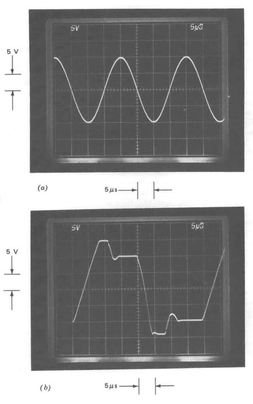
Figure 13.48 Large-signal performance of unity-gain inverter with two-pole compensation. (\(a\)) Sine-wave input. (\(b\)) Square-wave input.
We might suspect that two-pole compensation could improve the slew rate because the network topology shown in Figure 13.19 has the property that the steady-state value of the current \(i_N\) is zero for any magnitude ramp of \(v_N\). The output using a \(30\ pF-15\ k\Omega-30\ pF\) two-pole compensating network (the values indicated earlier in Figure 13.21) with the inverter connection is shown in Figure 13.48\(a\) for a 20-volt peak-to-peak, 50 kHz sine-wave input signal. The maximum slew rate demonstrated in this photograph is ap proximately 3.1 volts per microsecond, a value approximately twice that obtained with a single \(15-pF\) compensating capacitor.
Unfortunately, the large negative phase shift close to the crossover frequency that results from two-pole compensation proves disastrous when saturation occurs because the system approaches the conditions necessary for conditional stability. The poor recovery from the overload that results with large-signal square-wave excitation is illustrated in Figure 13.48\(b\). The collector-to-base junctions of the second-stage transistors are forward biased during part of the cycle because of the overshoot, and the resultant charge storage further delays recovery from overload.
It is of passing interest to note that the circuit using two-pole compensation exhibits a phenomenon called jump resonance. If the frequency of the 20-volt peak-to-peak sinusoid is raised slightly above the 50-kHz value used in Figure 13.48\(a\), the output signal becomes severely distorted. Further increases in excitation frequency result in an abrupt jump to a new mode of limiting with a recognizably different (though equally distorted) output signal. The process exhibits hysteresis, in that it is necessary to lower the excitation frequency measurably below the original jump value to reestablish the first type of nonlinear output signal. One of the few known virtues of jump resonance is that it can serve as the basis for very difficult academic problems in advanced describing-function analysis.(G. J. Thaler and M. P. Pastel, Analysis and Design of Nonlinear Feedback Control Systems, McGraw-Hill, New York, 1962, pp. 221-225. )
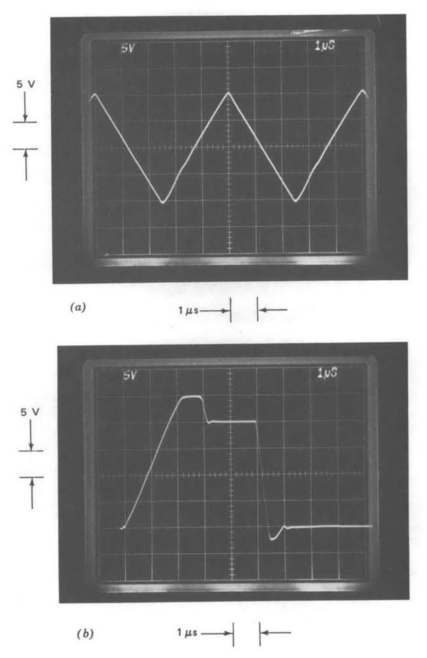
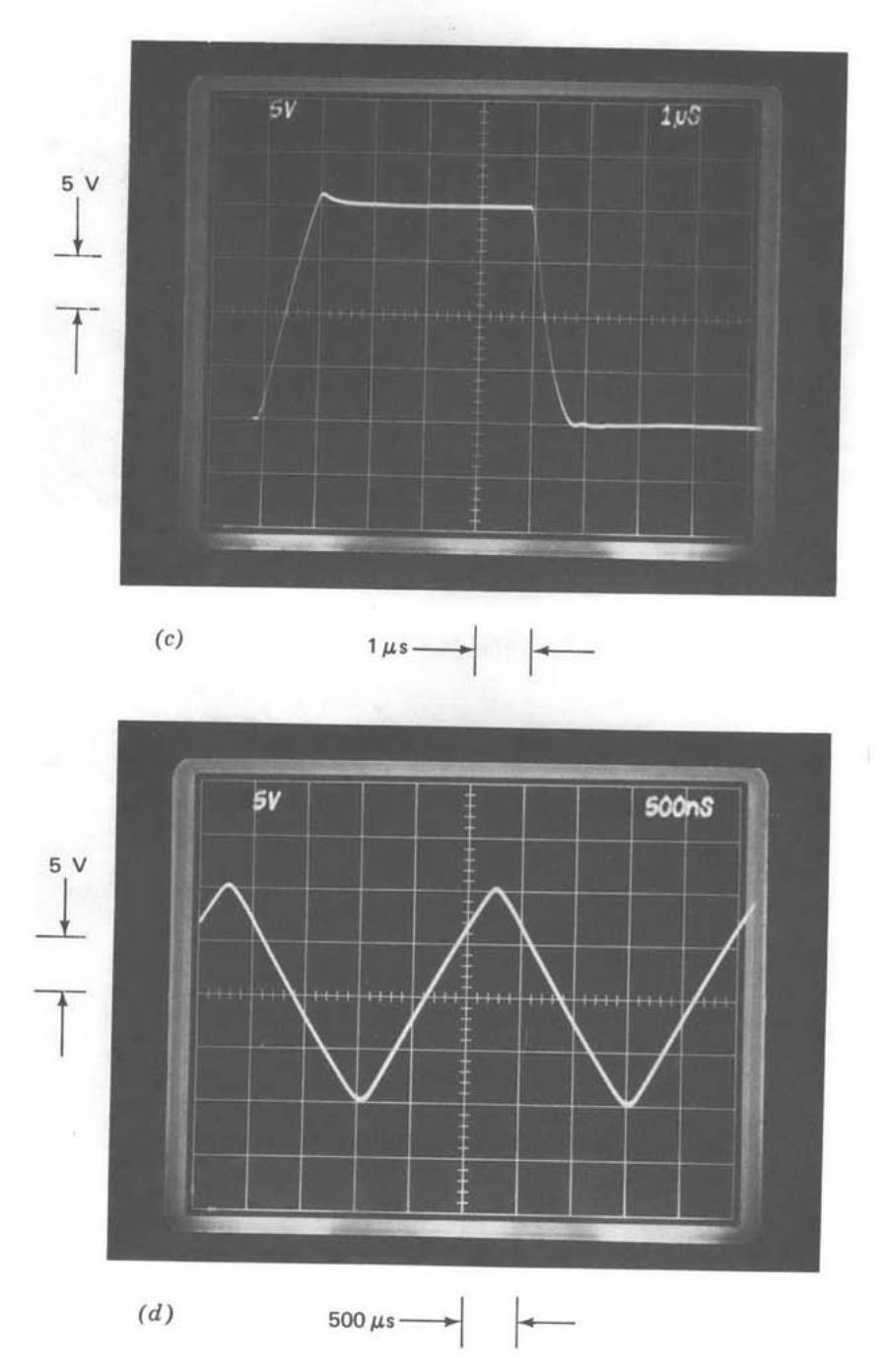
Figure 13.49 Slew rate of inverter with feed-forward compensation. (\(a\)) Triangle-wave input. (\(b\)) Square-wave input. (\(c\)) Square-wave input with increased second-stage bias current. (\(d\)) Triangle-wave input with increased second-stage current.
Feedforward compensation results in a high value for slew rate because capacitive feedback around the second stage is eliminated. The response of the inverter with \(150-pF\) feedforward compensation to a 20-volt peak-to peak, 200-kHz triangle wave is shown in Figure 13.49\(a\). While some distortion is evident in this photograph, the amount is not excessive considering that a slew rate of 8 volts per microsecond is achieved. The square-wave response shown in Figure 13.49b indicates problems similar to those associated with two-pole compensation. The response also indicates that the negative slew rate is substantially faster than the positive slew rate with this compensation. The reason for the nonsymmetry is that with feedforward compensation, the slew rate of the amplifier is limited by the current available to charge the node at the output of the second stage (the collector of \(Q_{10}\) in Figure 10.19). The current to charge this node in a negative direction is derived from \(Q_{10}\), and relatively large currents are possible from this device. Conversely, postive slew rate is established by the relatively lower bias currents available. The way to improve symmetry is to increase the collector bias current of \(Q_{10}\). While this increase could be accomplished with an external current source applied via a compensation terminal, a simpler method is available because of the relationship between the voltage at the collector of \(Q_{10}\) and the output voltage of the amplifier. Level shifting in the buffer stage raises the output voltage one diode potential above the collector voltage of \(Q_{10}\) in the absence of load. If a resistor is connected between the amplifier output and the compensation terminal at the output of second stage, the resistor will act like a current source because the voltage across it is "bootstrapped" by the buffer amplifier. Furthermore, the level shift in the buffer is of the correct polarity to improve slew-rate symmetry when the resistor is used.
The square-wave response of Figure 13.49\(c\) illustrates the performance of the inverter with feedforward compensation when a \(1-k\Omega\) resistor is connected from the amplifier output to the collector side of the second stage. The positive-going slew rate is increased to approximately 20 volts per microsecond. Furthermore, the overload recovery characteristics improve, probably as a result of better second-stage dynamics at higher bias currents. The response to a 400-kHz triangle wave with feedforward compensation and increased bias current is illustrated in Figure 13.49\(d\). This signal is reasonably free of distortion and has a slew rate of 16 volts per microsecond.
While the method of combining feedforward compensation with in creased operating levels is not necessarily recommended for routine use, it does illustrate the flexibility that often accompanies the availability of external compensating terminals. In this case, it is possible to raise the dy namic performance of an inexpensive, general-purpose integrated-circuit amplifier to levels usually associated with more specialized wideband units by means of appropriate connections to the compensating terminals.
Summary
The material presented earlier in this section has given some indication of the power and versatility associated with the use of minor-loop compensation for two-stage operational amplifiers. We should recognize that the relative merits of various forms of open-loop transfer functions remain the same regardless of details specific to a particular feedback system. For example, tachometric feedback is often used around a motor-amplifier combination to form a minor loop included as part of a servomechanism. This type of compensation is entirely analogous to using a minor-loop feedback capacitor for one-pole compensation. Similarly, if a tachometer is followed with a high-pass network, two-pole minor-loop compensation results. It should also be noted that in many cases transfer functions similar to those obtained with minor-loop compensation can be generated via forward- path compensation.
While the compensation networks have been illustrated in connections that use relatively simple major-loop feedback networks, this limitation is unnecessary. There are many sophisticated systems that use operational amplifiers to provide gain and to generate compensating transfer functions for other complex elements. The necessary transfer functions can often be realized either with major-loop feedback around the operational amplifier, or by compensating the amplifier to have an open-loop transfer function of the required form. The former approach results in somewhat more stable transfer functions since it is relatively less influenced by amplifier parameters, while the latter often requires fewer components, particularly when a differential-input connection is necessary.
It is emphasized that a fair amount of experience with a particular amplifier is required to obtain the maximum performance from it in demanding applications. Quantities such as the upper limit to crossover frequency for reliably stable operation and the uncompensated open-loop transfer function are best determined experimentally. Furthermore, many amplifiers have peculiarities that, once understood, can be exploited to enhance performance. The feedforward connection used with the LM101A is an example. Another example is that the performance of certain amplifiers is enhanced when the compensating network (or some portion of the compensation) is connected to the output of the complete amplifier rather than to the output of the high-gain stage because effects of loading by the network are reduced and because more of the amplifier is included inside the minor loop. The time a system designer spends understanding the subtleties of a particular amplifier is well rewarded in terms of the performance that he can obtain from the device.
Important features of the various types of compensation discussed in this section are summarized in Table 13.1. This table indicates the open-loop transfer functions obtained with the different compensations. The solid lines represent regions where the transfer function is controlled by the compensating network, while dotted lines are used when uncompensated amplifier characteristics dominate. The minor-loop feedback networks used to obtain the various transfer functions from two-stage amplifiers are also shown. Comments indicating relative advantages and disadvantages are included.
Table 13.1 Implementation and Effects of Various Types of Compensation
| One Pole | |
| Transfer Function | Network |
 |
 |
|
Conservative, general-purpose compensation for systems with frequency-independent feedback and loading. Changing capacitor value optimizes bandwidth as a function of attenuation provided by feedback network. Slew rate inversely proportional to capacitor size. |
|
| Two Pole | |
| Transfer Function | Network |
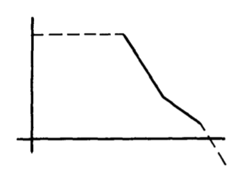 |
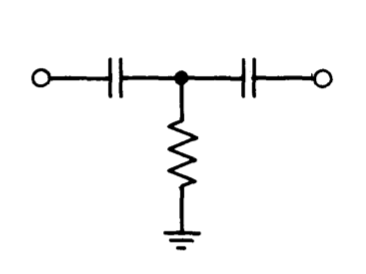 |
|
Improved desensitivity and lower error coefficients compared with one-pole systems with identical crossover frequencies. Loop parameters must be selected to insure that crossover occurs in the \(1/s\) region of the characteristics for adequate stability. Instability generally results with capacitive loading or low-pass major-loop feedback networks. Poor recovery from overload. |
|
| With Zero | |
| Transfer Function | Network |
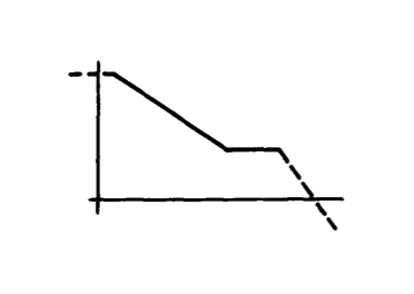 |
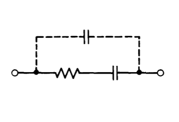 |
|
Zero is used to offset effects of pole associated with load or feedback network, and must be located as a function of this pole. Major loop becomes unstable if pole is eliminated. A small-value capacitor, indicated with dotted lines, improves minor-loop stability. |
|
| Slow Rolloff | |
| Transfer Function | Network |
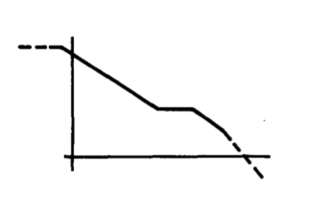 |
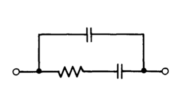 |
|
Useful for systems with an additional loop-transmission pole at an uncertain location. Adding more rungs to ladder network increases the range of frequencies over which the additional pole can be located and results in greater uniformity of phase-shift characteristics. Prolonged settling time compared to one-pole compensation when additional loop-transmission pole not present. |
|
| Feedforward | |
| Transfer Function | Typology |
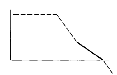 |
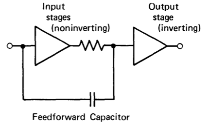 |
|
Highest bandwidth. Most useful when bandwidth of first stage or stages is less than that of rest of amplifier. Can result in substantial slew-rate improvement. Limits amplifier to use in inverting connections only. Values and results critically dependent on specific details of amplifier performance. Sensitive to capacitive loading or other sources of nega tive loop-transmission phase shift. |
|
Exercise \(\PageIndex{1}\)
An operational amplifier is available with a fixed, unloaded open-loop transfer function
\[a(s) \simeq \dfrac{10^5}{10^{-2} s + 1}.\nonumber \]
This amplifier is to be used as a unity-gain inverter. A load capacitor adds a pole at \(s = -10^6\text{ sec}^{-1}\) to the unloaded open-loop transfer function. Compensate this configuration with an input lead network so that its loop-transmission magnitude is inversely proportional to frequency from low frequencies to a factor of five beyond the crossover frequency. Choose element values to maximize crossover frequency subject to this constraint. You may assume high input impedance for the amplifier.
Exercise \(\PageIndex{2}\)
Design an input lag network and an input lead-lag network to compensate the capacitively loaded inverter described in Exercise \(\PageIndex{1}\). Maximize crossover frequency for your designs subject to the constraint that the loop transmission is inversely proportional to frequency over a frequency range that extends from a factor of five below to a factor of five above the crossover frequency.
Exercise \(\PageIndex{3}\)
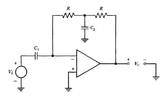
Figure 13.50 Double differentiator.
An operational amplifier is connected as shown in Figure 13.50 in an attempt to obtain a closed-loop transfer function
\[\dfrac{V_o (s)}{V_i (s)} = -s (0.1s + 1)\nonumber \]
Determine element values that yield an ideal closed-loop gain given by this expression.
Measurements indicate that the open-loop transfer function of the amplifier is approximately single pole and that the transfer-function magnitude is \(10^4\) at \(\omega = 10^3\) radians per second. Needless to say, the configuration shown in Figure 13.50 is hopelessly unstable with this amplifier.
Find appropriate topological modifications that will stabilize the system (without changing the amplifier) and will result in a closed-loop transfer function that approximates the desired one at frequencies below 100 radians per second.
Exercise \(\PageIndex{4}\)
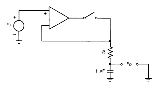
Figure 13.51 Sample-and-hold circuit.
A sample-and-hold circuit is constructed as shown in Figure 13.51. The unloaded open-loop transfer function of the amplifier is
\[a(s) \simeq \dfrac{10^6}{(0.1s + 1)(10^{-7} s + 1)}\nonumber \]
The sum of the open-loop output resistance of the amplifier and the on resistance of the switch is \(100\ \Omega\).
(a) With \(R = 0\), is this circuit stable in the sample mode (switch closed)?
(b) Determine a value for \(R\) that results in approximately \(45^{\circ}\) of phase margin in the sample mode.
(c) Estimate the time required for \(v_O (t)\) to reach 1% of final value following initiation of sampling when the value of \(R\) determined in part \(b\) is used. You may assume that the capacitor is initially discharged, that \(v_I\) is time invariant, and that the circuit remains linear during the transient.
Exercise \(\PageIndex{5}\)
An externally compensated operational amplifier that uses minor-loop feedback to generate an approximate open-loop transfer function
\[a(s) \simeq \dfrac{2 \times 10^{-4}}{Y_c (s)}\nonumber \]
is available. The amplifier is connected as a unity-gain voltage follower. The spectral content of anticipated input signals is such that a closed-loop bandwidth in excess of \(10^6\) radians per second degrades the noise performance of the connection. Determine a compensating element that will result in a closed-loop transfer function
\[A(s) \simeq \dfrac{1}{10^{-6} s + 1} \nonumber \]
for the voltage-follower connection.
Exercise \(\PageIndex{6}\)
An operational amplifier of the type described in Exercise \(\PageIndex{5}\) is connected in the log circuit shown in Figure 13.9\(a\). Experimental evaluation shows that this connection will be acceptably stable if the loop crossover frequency is limited to 1 MHz. Determine a compensating element that insures stability for any input-signal level between 0 and +10 volts. Estimate the time required for the incremental output signal of the circuit to settle to 1% of final value when a small step change in input voltage is applied at an operating point \(V_I = 0.1\) volt.
Exercise \(\PageIndex{7}\)
A two-stage operational amplifier has a d-c open-loop gain of \(10^6\) and is acceptably stable in connections involving frequency-independent feedback provided that compensation is selected which limits the crossover frequency to 1 MHz. This amplifier is used as a unity-gain inverter to amplify 10-kHz sinusoids, and a major design objective is to have the input and the output signals of the inverter exactly \(180^{\circ}\) out of phase. Discuss the relative merits of one- and two-pole compensation in this
application. Also indicate the effect that the two types of compensation have on the magnitude of the closed-loop transfer function at 10 kHz.
Exercise \(\PageIndex{8}\)
The uncompensated, open-loop transfer function of a two-stage amplifier is
\[a(s) = \dfrac{10^5}{(10^{-4} s + 1)(10^{-5} s + 1)(5 \times 10^{-8} s + 1)^2} \nonumber \]
The two lowest-frequency poles result from dynamics that can be modified by compensation, while the location of the higher-frequency pole pair is independent of the compensation that is used.
The amplifier is compensated and connected for a noninverting gain of 10. You may assume that the compensation used does not cause significant loading of the minor loop. This closed-loop connection is excited with an input ramp having a slope of \(10^4\) volts per second. The differential input signal applied to the amplifier is observed, and it is found that after a starting transient, the steady-state value of the signal is \(10\ mV\).
(a) Determine a single-pole approximation to the amplifier open-loop transfer function.
(b) Refine your estimate of part a, taking advantage of all the information you have available about the amplifier.
(c) Assuming that this amplifier described is an LM301A, what compensating element is used?
(d) Suggest alternate compensation that results in the same crossover frequency as obtained with the compensation described, a phase margin in excess of \(60^{\circ}\), and essentially zero steady-state ramp error. Determine element values that implement the required compensation for an LM301A.
Exercise \(\PageIndex{9}\)
The material discussed in connection with Figure 13.24 indicated that the steady-state error of a closed-loop operational-amplifier connection in response to a ramp can be reduced to insignificant levels by using two-pole compensation. An extension of this line of reasoning implies that if three-pole compensation is used, the steady-state error will be nearly zero for parabolic excitation. Linear-system considerations show that stability is possible if two zeros are combined with a three-pole rolloff. For example, a loop transmission
\[L(s) = -\dfrac{10^{16} (10^{-5} s + 1)^2}{s^3} \nonumber \]
has approximately \(80^{\circ}\) of phase margin at its crossover frequency.
Find a compensating-network topology that can be used in conjunction with minor-loop compensated amplifiers to provide this general type of open-loop transfer function. Discuss practical difficulties you anticipate with this form of transfer function.
Exercise \(\PageIndex{10}\)
A two-stage operational amplifier that uses minor-loop compensation is loaded with a capacitor that adds a pole at \(s = -10^6\text{ sec}^{-1}\) to the unloaded open-loop transfer function of the amplifier. The desired open-loop transfer function including loading effects is
\[a(s) \simeq \dfrac{2 \times 10^{11} (5 \times 10^{-6} s + 1)}{s^2} \nonumber \]
Find a compensating-network topology that can be used to effect this form of compensation. Determine appropriate element values assuming that the effective input-stage transconductance of the operational amplifier used is \(2 \times 10^{-4}\) mho.
Exercise \(\PageIndex{11}\)
A two-stage operational amplifier is connected as an inverting differentiator with a feedback resistor of \(100\ k\Omega\) and an input capacitor of \(1\ \mu F\). What type of minor-loop compensating network should be used to stabilize this configuration? Determine element values that result in a predicted crossover frequency of \(10^4\) radians per second with a value of \(2 \times 10^{-4}\) mho for input-stage transconductance.
When this type of compensation is tried using an LM301A operational amplifier, minor loop stability is unacceptable, and it is necessary to shunt the compensation terminals with a \(3-pF\) capacitor in addition to the network developed above for satisfactory performance. Describe the effect of this modification on closed-loop performance.
Exercise \(\PageIndex{12}\)
A certain application necessitates an operational amplifier with an ap proximate open-loop transfer function
\[a(s) \simeq \dfrac{10^4}{s^{2/3}} \nonumber \]
Find a compensating network that can be used in conjunction with an LM301A to approximate this transfer function. The phase shift of the approximating transfer function should be \(- 60^{\circ} \pm 5^{\circ}\) over a frequency range from 1 radian per second to \(10^6\) radians per second.