
7.3: Wave Shaping
- Page ID
- 3588

7.3.1: Active Clampers
Clampers are used to add a specific amount of DC to a signal. Generally, the amount of DC will be equal to the peak value of the signal. Clampers are intelligent in that they can adjust the amount of DC if the peak value of the input signal changes. Ideally, clampers will not change the shape of the input signal; rather, the output signal is simply a “vertically shifted” version of the input, as shown in Figure \(\PageIndex{1}\). One common application of the clamper is in television receivers. Here, a clamper is referred to as a DC restorer. Certain portions of the video signal, such as sync pulses, are required to be at specific levels. After the video signal has been amplified by AC coupled gain stages, the DC restorer returns the video to its normal orientation. Without the clamping action, the various parts of the signal cannot be decoded properly. Clampers are commonly made with passive components, just as rectifiers are. Like rectifiers, simple clampers produce errors caused by the diode's forward voltage drop. Active clampers remove this error.
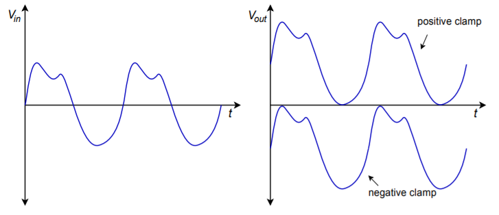
Figure \(\PageIndex{1}\): Effect of clampers on input signal a. input signal (left) b. clamped outputs (right).
Conceptually, a clamper needs to sense the amplitude of the input signal and create a DC signal of equal value. This DC signal is then added to the input, as shown in Figure \(\PageIndex{2}\). If the peak value is known, and does not change, it is possible to create this function with a summing amplifier. If the signal level is dynamic, a different course needs to be taken. The trick is in getting the DC source to properly track input level changes. Obviously, a simple DC supply is not appropriate; however, a charged capacitor will fit the bill nicely - as long as its discharge time constant is much longer than the period of the input wave. All that needs to be done is to have the capacitor charge to the peak level of the input. When the capacitor voltage is added to the input signal, the appropriate DC shift will result.
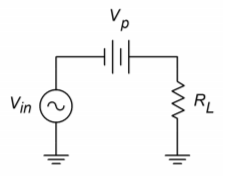
Figure \(\PageIndex{2}\): Simple clamper model.
Figure \(\PageIndex{3}\) shows an active positive clamper. On the first negative going peak of the input, the source will attempt to pull current through the capacitor in the direction shown. This forces the inverting input of the op amp to go slightly negative, thus creating a positive op amp output. The result of this action will be to forward-bias the diode and supply charging current to the capacitor. The capacitor will charge to the negative peak value of the input. The output resistance of the op amp is very low, so charging is relatively fast, only being limited by the maximum output current of the op amp. When the source changes direction, the op amp will produce a negative output, thus turning off the diode and effectively removing the op amp from the circuit. Because the discharge time for \(C\) is much longer than the input period, its potential stays at roughly \(V_{p-}\). It now acts like a voltage source. These two sources add, so we can see that the output must be:
\[ V_{out} = V_{in} + |V_{p-}| \label{7.1} \]
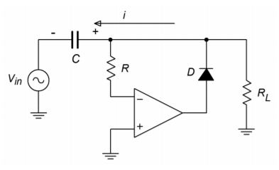
Figure \(\PageIndex{3}\): Active positive clamper.
The op amp will remain in saturation until the next negative peak, at which point the capacitor will be recharged. During the charging period, the feedback loop is closed, and thus, the diode's forward drop is compensated for by the op amp. In other words, the op amp's output will be approximately 0.6 to 0.7 V above the inverting input's potential. The discharge time of the circuit is set by the load resistor, \(R_l\). If particularly long time constants are required, a buffer stage may be used, along with an FET input clamping op amp. The resistor \(R\) is used to prevent possible damage to the op amp from capacitor discharge. This value is normally in the low kilohm region. In order to make a negative clamper, just reverse the polarity of the diode.
Sometimes, it is desirable to clamp a signal and add a fixed offset as well. An example output waveform of this type is shown in Figure \(\PageIndex{4}\).
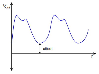
Figure \(\PageIndex{4}\): Clamped output with offset.
This function is relatively easy to add to the basic clamper. In order to include the offset, all that needs to be done is to change the op amp's reference point. In the basic clamper, the noninverting input is tied to ground. Consequently, this establishes the point at which the charge/discharge cycle starts. If this reference is altered, the charge/discharge point is altered too. To create a positive offset, a DC signal equal to the offset is applied to the noninverting input, as shown in Figure \(\PageIndex{5}\). A similar arrangement may be used for negative clampers.
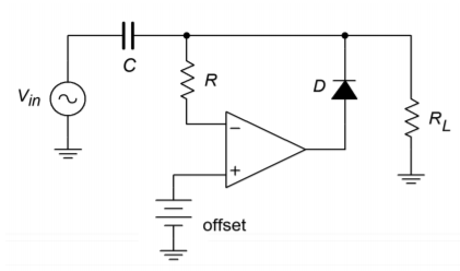
Figure \(\PageIndex{5}\): Active positive clamper with offset.
Example \(\PageIndex{1}\)
An active clamper is shown in Figure \(\PageIndex{6}\). An LF412 op amp is used (a dual LF411). Determine the capacitor's voltage and verify that the time constant is appropriate for the input waveform. Also, sketch the output waveform and determine the maximum differential input voltage for the first op amp.
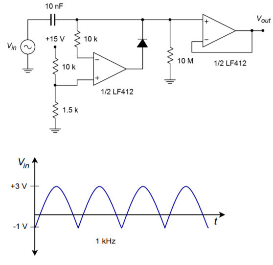
Figure \(\PageIndex{6}\): Active clamper circuit (top) and input waveform (bottom) for Example \(\PageIndex{1}\).
Because this is a positive clamper, the capacitor's voltage is the sum of the offset potential and the negative peak potential of the input waveform. \(V_{offset}\) is set by the 10 k\(\Omega\)/1.5 k\(\Omega\) divider.
\[ V_{offset} = V_{CC} \frac{R_2}{R_1+R_2} \nonumber \]
\[ V_{offset} = 15 V \frac{1.5 k}{10 k+1.5 k} \nonumber \]
\[ V_{offset} = 1.96 V \nonumber \]
\[ V_c = V_{offset} + |V_{p-}| \nonumber \]
\[ V_c = 1.96 V+|−1 V| \nonumber \]
\[ V_c = 2.96 V \nonumber \]
This is the amount of DC added to the input signal. The output waveform will look just like the input, except that it will be shifted up by 2.96 V. This is shown in Figure \(\PageIndex{7}\).
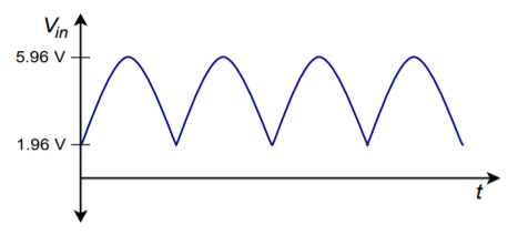
Figure \(\PageIndex{7}\): Output of clamper for Example \(\PageIndex{1}\).
The discharge time constant should be much larger than the period of the input wave. The input wave has a frequency of 1 kHz, and thus, a period of 1 ms. The capacitor discharges through the load resistor. As FET input op amps are used, their effect on the discharge rate is minimal.
\[ T = R_l C \nonumber \]
\[ T = 10 M\times 10nF \nonumber \]
\[ T = 0.1s \nonumber \]
The discharge rate is 100 times longer than the input period, so the capacitor droop will be satisfactory.
The maximum differential input signal is the worst-case difference between the inverting and noninverting input potentials. The noninverting input is tied directly to 1.96 V. The inverting input sees the output waveform. The maximum value of the output is 5.96 V. So the difference is
\[ V_{in-diff} = V_{in +} − V_{in -} \nonumber \]
\[ V_{in-diff} = 1.96 V−5.96 V \nonumber \]
\[ V_{in-diff} = −4 V \nonumber \]
The LF412 will have no problem with a differential input of this size.
Computer Simulation
A simulation of the clamper circuit of Example \(\PageIndex{1}\) is shown in Figure \(\PageIndex{8}\). In order to simplify the simulation somewhat, the input signal has been altered modestly. Instead of the shifted 4 volt peak-to-peak full-wave rectified signal originally used, a shifted 4 volt peak-to-peak sine wave is used.
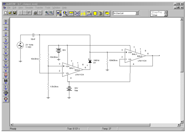
Figure \(\PageIndex{8a}\): Clamper schematic in Multisim.
Both the input and output waveforms are plotted in the Transient Analysis. The circuit requires about 1 cycle of the waveform before the output stabilizes. After that point the clamping action and shift of nearly 2 volts is quite evident in the output waveform. There is no noticeable droop, scaling error, or obvious distortion in the output either, although some minor aberrations can be seen at the negative peaks on occasion.
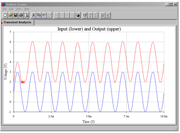
Figure \(\PageIndex{8b}\): Clamper waveforms.
7.3.2: Active Limiters
A limiter is a circuit that places a maximum restriction on its output level. The output of a limiter can never be above a specific preset level. In one sense, all active circuits are limiters, in that they will all eventually clip the signal by going into saturation. A true limiter, though, prohibits the signal at levels considerably lower than saturation. The exact level is fairly easy to set. Limiters can be used to protect following stages from excessive input levels. They can also be seen as a type of wave shaper. One form of limiter was shown in Chapter Six, in the Pocket Rockit's schematic. In that circuit, a limiter was used to purposely clip the music signal for artistic effect. The limitation of that form is that the limit potential is locked at \(\pm\).7 V by the parallel signal diodes. For a more general form, an arbitrary limit potential is desired. Instead of using parallel signal diodes, a series combination of Zener diodes will prove useful.
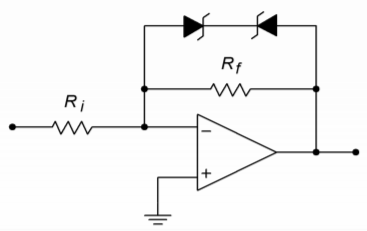
Figure \(\PageIndex{9}\): Active limiter.
An example limiter is shown in Figure \(\PageIndex{9}\). It is based upon the inverting voltage amplifier form. As long as the output signal is below the Zener potential, the output equals the input times the voltage gain. If the output voltage tries to rise above the Zener potential, one of the diodes will go into Zener conduction, and the other diode will go into forward bias. Once this happens, the low dynamic resistance of the diodes will disallow any further increase in output potential. The output will not be allowed to move outside of the Zener potential (plus the 0.7 V turn-on for the second diode):
\[ |V_{out}| \leq V_{zener} + 0.7V \label{7.2} \]
Or we might reword this as
\[ V_{limit} = \pm (V_{zener} + 0.7 V) \label{7.3} \]
This effect is shown graphically in Figure \(\PageIndex{10}\), the limiter's transfer characteristic.
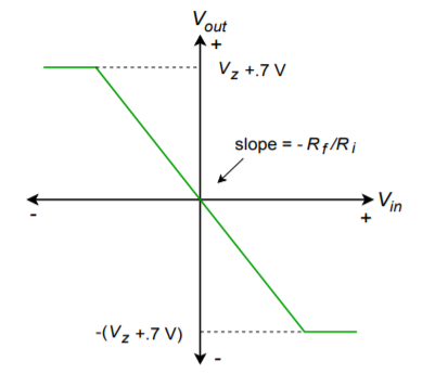
Figure \(\PageIndex{10}\): Transfer characteristic of limiter.
Example \(\PageIndex{2}\)
If the input to the circuit of Figure \(\PageIndex{11}\) is a 4 V peak triangle wave, sketch \(V_{out}\).
Without the Zener limit diodes, this amplifier would simply multiply the input by a gain of two and invert it.
\[ V_{out} = A_v V_{in} \nonumber \]
\[ V_{out} = −2\times 4 V (peak) \nonumber \]
\[ V_{out} = −8V (peak) \nonumber \]
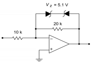
Figure \(\PageIndex{11}\): Limiter for Example \(\PageIndex{2}\).
So, an inverted 8 V peak triangle would be the output. With the inclusion of the diodes, the maximum output is
\[ V_{limit} = \pm (V_{zener} + 0.7 V) \nonumber \]
\[ V_{limit} = \pm (5.1 V + 0.7 V) \nonumber \]
\[ V_{limit} = \pm 5.8 V \nonumber \]
Consequently, the output wave is clipped at 5.8 V, as shown in Figure \(\PageIndex{12}\).
By using different Zeners, it is also possible to produce asymmetrical limiting. For example, positive signals might be limited to 10 V, whereas negative signals could be limited to -5 V.
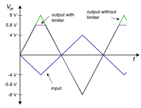
Figure \(\PageIndex{12}\): Input/output signals of limiter for Example \(\PageIndex{2}\).