
7.5: Comparators
- Page ID
- 3590

The simple open-loop op amp comparator was discussed in Chapter 2. Although this circuit is functional, it is not the final word on comparators. It suffers from two faults: (1) it is not particularly fast, and (2) it does not use hysteresis. Hysteresis provides a margin of safety and “cleans up” switching transitions. Providing a comparator with hysteresis means that its reference depends on its output state. As an example, for a positive going transition, the reference might be 2 V, but for a negative transition, the reference might be 1 V. This effect can dramatically improve performance when used with noisy inputs.
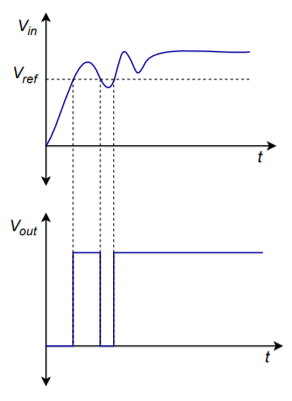
Figure \(\PageIndex{1}\): False turn-off spike.
Take a look at the noisy signal in Figure \(\PageIndex{1}\). If this signal is fed into a simple comparator, the noise will produce a false turn-off spike. If this same signal is fed into a comparator with hysteresis, as in Figure \(\PageIndex{2}\), a clean transition results. In order to change from low to high, the signal must exceed the upper reference. In order to change from high to low, the signal must drop below the lower reference. This is a very useful feature. A comparator with hysteresis is shown in Figure \(\PageIndex{3}\).
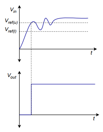
Figure \(\PageIndex{2}\): Clean transition using hysteresis.
The output voltage of this circuit will be either +\(V_{sat}\) or -\(V_{sat}\). Let's assume that the device is at -\(V_{sat}\). In order to change to +\(V_{sat}\), the inverting input must go lower than the noninverting input. The noninverting input is derived from the \(R_1/R_2\) voltage divider. The divider is driven by the output of the op amp, in this case, -\(V_{sat}\). Therefore, to change state, \(V_{in}\) must be
\[ V_{in} = V_{\text{lower thres}} = −V_{sat} \frac{R_2}{R_1+R_2} \label{7.4} \]
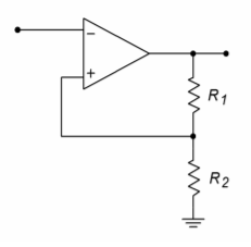
Figure \(\PageIndex{3}\): Comparator with hysteresis.
Similarly, to go from positive to negative,
\[ V_{in} = V_{\text{upper thres}} = + V_{sat} \frac{R_2}{R_1+R_2} \label{7.5} \]
The upper and lower trip points are commonly referred to as the upper and lower thresholds. The adjustment of \(R_1\) and \(R_2\) creates an “error band” around zero (ground). Note that when the trip point is reached, the comparator output state changes, thus changing the reference. This reinforces the initial change. In effect, the comparator is now using positive feedback (note how the feedback signal is tied to the noninverting terminal). This circuit is sometimes referred to as a Schmitt Trigger. A noninverting version of the Schmitt Trigger is shown in Figure \(\PageIndex{4}\). Note that in order to change state, the noninverting terminal's voltage will be approximately zero. If the circuit is in the low state, the voltage across \(R_1\) will equal -\(V_{sat}\) at the time of transition. At this point, the voltage across \(R_2\) will equal \(V_{in}\). The current into the op amp is negligible, so the current through \(R_1\) equals that through \(R_2\).
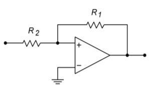
Figure \(\PageIndex{4}\): Noninverting comparator with hysteresis
\[V_{R1} R_1 = V_{R2}{R_2} \nonumber \]
\[ -\frac{(−V_{sat})}{R_1} = \frac{V_{in}}{R_2} \nonumber \]
Because \(V_{in}\) equals the threshold voltage at transition,
\[ V_{in} = V_{\text{upper thres}} = V_{sat} \frac{R_2}{R_1} \label{7.6} \]
Similarly, for the opposite transition,
\[ V_{in} = V_{\text{lower thres}} = −V_{sat} \frac{R_2}{R_1} \label{7.7} \]
Example \(\PageIndex{1}\)
Sketch the output waveform for the circuit of Figure \(\PageIndex{5}\) if the input signal is a 5 V peak sine wave.
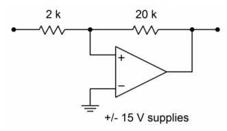
Figure \(\PageIndex{5}\): Comparator for Example \(\PageIndex{1}\).
First, determine the upper and lower threshold voltages.
\[ V_{upper \ thres} = V_{sat} \frac{R_2}{R_1} \nonumber \]
\[ V_{upper \ thres} = 13 V \frac{2k}{20 k} \nonumber \]
\[ V_{upper \ thres} = 1.3 V \nonumber \]
\[ V_{lower \ thres} = −V_{sat} \frac{R_2}{R_1} \nonumber \]
\[ V_{lower \ thres} = −13 V \frac{2 k}{20 k} \nonumber \]
\[ V_{lower \ thres} = −1.3 V \nonumber \]
The output will go to +13 V when the input exceeds +1.3 V and will go to -13 V when the input drops to -1.3 V. The input/output waveform sketches are shown in Figure \(\PageIndex{6}\).
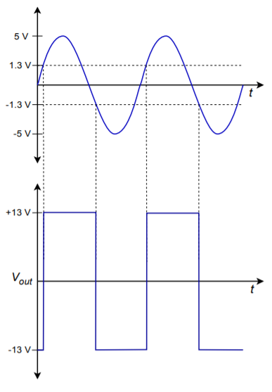
Figure \(\PageIndex{6}\): Comparator waveforms.
Computer Simulation
In Figure \(\PageIndex{7}\), a simulation of the circuit and waveforms of Example \(\PageIndex{1}\) are shown using Multisim. A reasonably fast op amp, the LF411, was chosen for the simulation in order to minimize slewing effects. The input and output waveforms are superimposed in the Transient Analysis. This allows the switching levels to be determined precisely. From the graph, it is very clear that the high-to-low output transition occurs when the input drops below about -1.3 volts. Similarly, the low-to-high transition occurs when the input rises above about 1.3 volts. This is exactly as expected, and it reinforces the concept of hysteresis visually. The other effect that may be noted here is an effective delaying of the pulse signal relative to the timing at the input's zero-crossings. This is an unfortunate side effect that is magnified by wide thresholds and slowing varying input signals.
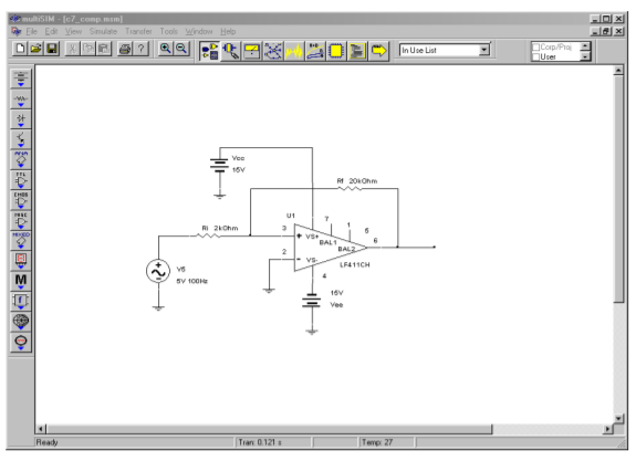
Figure \(\PageIndex{7a}\): Simulation of comparator.
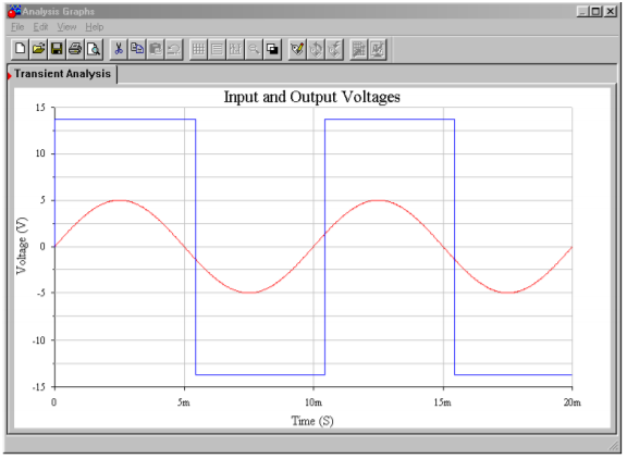
Figure \(\PageIndex{7b}\): Comparator waveforms.
Although the use of positive feedback and hysteresis is a step forward, switching speed is still dependent on the speed of the op amp. Also, the output levels are approximately equal to the power supply rails, so interfacing to other circuitry (such as TTL logic) requires extra circuitry. To cure these problems, specialized comparators circuits have evolved. Generally, comparator ICs can be broken down into a few major categories: general-purpose, high speed, and low power/low cost. A typical general-purpose device is the LM311, whereas the LM360 is a high-speed device with differential outputs. Examples of the low power variety include the LM393 dual comparator and the LM339 quad comparator. As was the case with ordinary op amps, there is a definite trade-off between comparator speed and power consumption. As you might guess, the high speed LM360 suffers from the highest power consumption, whereas the more miserly LM393 and LM339 exhibit considerably slower switching speeds. High-speed devices often exhibit high input bias and offset currents as well.
The general-purpose LM311 is one of the more popular comparators in use today. An FET input version, the LF311, is also available. Generally, all of the op amp-based comparator circuits already mentioned can be adapted for use with the LM311. The LM311 is far more flexible than the average op amp comparator, however. An outline and data sheet for the LM311 are shown in Figures \(\PageIndex{8a}\) and \(\PageIndex{8b}\).
First of all, note that the LM311 is reasonably fast, producing a response time of approximately 200 ns. This places it in squarely in the middle performance range, as it is 10 or so times faster than a low-power comparator, but at least 10 times slower than high-speed devices. The voltage gain is relatively high, at 200,000 typically. Input offset voltage is moderate at 0.7 mV typically, and 3.0 mV maximum, at room temperature. The input offset and bias currents are 10 nA and 100 nA worst case, respectively. Devices with improved offset and bias performance are available, but these values are acceptable for most applications. (For example, the FET input LF311 shows input offset and bias currents of about 1000 times less, with only a slight increase in worst case input offset voltage.) The saturation voltage indicates exactly how low a “low state” potential really is. For a typical TTL-type load, the LM311 low output will be no more than 400 mV. Finally, note the current draw from the power supplies. Worst-case values are 6.0 mA and 5.0 mA from the positive and negative supplies, respectively. By comparison, low-power comparators are normally in the 1 mA range, whereas high-speed devices can range up toward 20 to 30 mA.
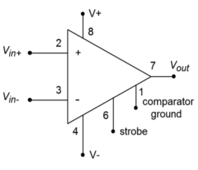
Figure \(\PageIndex{8a}\): The LM311comparator.
The LM311 may be configured to drive TTL or MOS logic circuits, and loads referenced to ground, the positive supply or the negative supply. Finally, it can directly drive relays or lamps with its 50 mA output current capability.
The operation of the LM311 is as follows:
- If \(V_{in+} > V_{in-}\) the output goes to an open collector condition. Therefore, a pull-up resistor is required to establish the high output potential. The pull-up does not have to go back to the same supply as the LM311. This aids in interfacing with various logic levels. For a TTL interface, the pull-up resistor will be tied back to the +5 V logic supply.
- If \(V_{in-} > V_{in+}\) the output will be shorted through to the “comparator ground” pin. Normally this pin goes to ground, indicating a low logic level of 0 V. It may be tied to other potentials if need be.
- The strobe pin affects the overall operation of the device. Normally, it is left open. If it is connected to ground through a current-limiting resistor, the output will go to the open-collector state regardless of the input levels. Normally, an LM311 is strobed with a logic pulse that turns on a switching transistor.
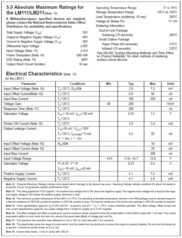
Figure \(\PageIndex{8b}\): LM311 data sheet. Reprinted courtesy of Texas Instrutments
An LM311 based comparator circuit is shown in Figure \(\PageIndex{9}\). It runs off of \(\pm\)15 V supplies so that the inputs are compatible with general op amp circuits. The output uses a +5 V pull-up source so that the output logic is TTL compatible. A small-signal transistor such as a 2N2222 is used to strobe the LM311. A logic low on the base of the transistor turns the transistor off, thus leaving the LM311 in normal operation mode. A high on the base will turn on the transistor, thus placing the LM311's output at a logic high.
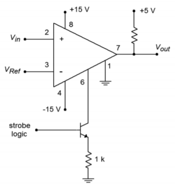
Figure \(\PageIndex{9}\): LM311 with strobe.
Our final type of comparator circuit is the window comparator. The window comparator is used to determine if a particular signal is within an allowable range of levels. This circuit features two different threshold inputs, an upper threshold, and a lower threshold. Do not confuse these items with the similarly named levels associated with Schmitt Triggers. A block diagram of a window comparator is shown in Figure \(\PageIndex{10}\).
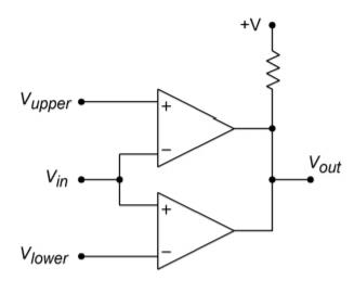
Figure \(\PageIndex{10}\): Window comparator
This circuit is comprised of two separate comparators, with common inputs and outputs. As long as the input signal is between the upper and lower thresholds, the output of both comparators will be high, thus producing a logic high at the circuit output. If the input signal is greater than the upper threshold or less than the lower threshold (i.e., outside of the allowed window), then one of the comparators will short its output to comparator ground, producing a logic low. The other comparator will go to an open collector condition. The net result is that the circuit output will be a logic low. Because the window comparator requires two separate comparators, a dual comparator package such as the LM319, can prove to be convenient.
An interesting application that uses comparators and function generation is shown in Figure \(\PageIndex{11}\). This is a single neuron from a pulse-coded continuous-time recurrent neural network.1 Neural networks are modeled after biological nervous systems and are used in a variety of applications such as robot motion control. Such networks may be implemented using digital or analog techniques, with advantages and disadvantages in each approach. This particular system is largely analog, although its final output is a pulse-width modulated square wave2. This avoids the signal attenuation problem that a pure analog approach might suffer from.
A complete system contains several neurons. Each neuron has a single output and several inputs. These inputs are fed from the outputs of the other neurons (including itself). The signals are weighted and then summed to create a composite excitation signal. The composite is summed with an offset or bias level, and then processed through a sigmoid function to produce the final output. In a pure analog scheme, the signals are just analog voltages. This scheme is a little different in that it uses pulse-width modulation to encode the signal levels. Low-level signals are represented as square waves with small duty cycles. High-level signals are represented via large duty cycles. One convenient aspect of this representation is that the signal is already in a form to directly control certain devices such as motors.
Let's follow the signal flow. The first stage is an adjustable gain inverting/noninverting amplifier, as seen in Chapter Four. The gain of this stage corresponds to the neuron weighting. Because the weighting can be either positive or negative, a simple potentiometer by itself is insufficient. The second stage is a fairly stock summing amplifier (also from Chapter Four). Its job is to combine the signals from the various weighted inputs. Its output is a very complicated-looking waveform: It is a combination of pulse-width modulated square waves, each with a different duty cycle and amplitude. The average “area under the curve” represents the overall signal strength. This is obtained via the adjustable RC network. The time constant is much slower than the base square wave frequency, so an averaging of the signal takes place. The output of op amp 3 is a smooth, slowly varying signal. This signal is combined with an adjustable offset bias and fed into the function generation circuit built around op amp 4. The gains and breakpoints are designed to mimic the compressive nature of the sigmoid function \(1/(1 + \varepsilon^{-x}\)). The resulting output level is then pulse coded. The pulse-width modulator is made from a simple triangle wave oscillator (covered in Chapter Nine) and a comparator. The amplitude range of the triangle wave precisely matches the range of signals expected from the sigmoid circuit. The larger the sigmoid output is, the longer the comparator output will be high. In other words, the duty cycle will follow the sigmoid circuit's output level, creating a pulse-width modulated signal. This output signal will be fed to the inputs of the other neurons in the network, and may also be used as one of the final desired output signals. For example, this signal may be used to drive one of the leg motors of a walking robot.
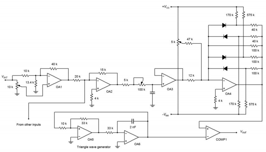
Figure \(\PageIndex{11}\): Pulse-coded continuous time recurrent neural network (single neuron shown).
References
1For further details on pulse-coded continuous-time recurrent neural networks, see Alan Murray and Lionel Tarassenko Analogue Neural VLSI - A Pulse Stream Approach (London: Chapman and Hall, 1994).
2See J.C. Gallagher and J.M. Fiore, “Continuous time recurrent neural networks: a paradigm for evolvalble analog controller circuits”, NAECON 2000