
7.6: Log and Anti-Log Amplifiers
- Page ID
- 3591

It is possible to design circuits with logarithmic response. The uses for this are many-fold. Recalling your logarithm fundamentals, remember that processes such as multiplication and division turn into addition and subtraction for logs. Also, powers and roots turn into multiplication and division. Bearing this in mind, if an input signal is processed by a logarithmic circuit, multiplied by a gain, \(A\), and then processed by an anti-log circuit, the signal will have effectively been raised to the \(A\)th power. This brings to light a great many possibilities. For example, in order to take the square root of a value, the signal would be passed through a log circuit, divided by two (perhaps with something as simple as a voltage divider), and then passed through an anti-log circuit. One possible application is in true RMS detection circuits. Other applications for log/anti-log amplifiers include signal compression and process control. Signals are often compressed in order to decrease their dynamic range (i.e., the difference between the highest and lowest level signals). In telecommunications systems, this may be required in order to achieve reasonable voice or data transmission with limited resources. Seeing their possible uses, our question then, is how do we design log/anti-log circuits?
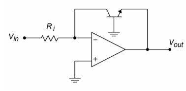
Figure \(\PageIndex{1}\): Basic log circuit.
Figure \(\PageIndex{1}\) shows a basic log circuit. The input voltage is turned into an input current by \(R_i\). This current feeds the transistor. Note that the output voltage appears across the base-emitter junction, \(V_{BE}\). The transistor is being used as a current-to-voltage converter. The voltage/current characteristic of a transistor is logarithmic, thus the circuit produces a log response. In order to find an output equation, we start with the basic Shockley Equation for PN junctions:
\[ I_c = I_s(\epsilon^{\frac{qV_{BE}}{K T}} −1) \label{7.8} \]
Where \(I_s\) is the reverse saturation current, \(\varepsilon\) is log base, \(q\) is the charge on one electron \(1.6\cdot 10^{-19}\) Coulombs, \(K\) is Boltzmann's constant 1.38∙10-23 Joules/Kelvin, and \(T\) is the absolute temperature in Kelvin.
Using 300K (approximately room temperature) and substituting these constants into Equation \ref{7.8} produces
\[ I_c = I_s (\epsilon^{38.6 V_{BE}} − 1 ) \label{7.9} \]
Normally, the exponent term is much larger than one, so this may be approximated as
\[ I_c = I_s \epsilon^{38.6 V_{BE}} \label{7.10} \]
Using the inverse log relationship and solving for \(V_{BE}\), this is reduced to
\[ V_{BE} = 0.0259 \ln \frac{I_c}{I_s} \label{7.11} \]
Earlier it was noted that the current \(I_c\) is a function of the input voltage and \(R_i\). Also, note that \(V_{out} = -V_{BE}\). Substituting these elements into Equation \ref{7.11} yields
\[ V_{out} = −0.0259 \ln \frac{V_{in}}{R_i I_s} \label{7.12} \]
We now have an amplifier that takes the log of the input voltage and also multiplies the result by a constant. It is very important that the anti-log circuit multiply by the reciprocal of this constant, or errors will be introduced. If the input voltage (or current) is plotted against the output voltage, the result will be a straight line if plotted on a semi-log graph, as shown in Figure 7.57. The rapid transition at approximately 0.6 V is due to the fast turn-on of the transistor's base-emitter junction. If output voltages greater than 0.6 V are required, amplifying stages will have to be added.
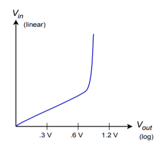
Figure \(\PageIndex{2}\): Input/output characteristic of log amplifier.
There are a couple of items to note about this circuit. First, the range of input signals is small. Large input currents will force the transistor into less-than-ideal logarithmic operation. Also, the input signal must be unipolar. Finally, the circuit is rather sensitive to temperature changes. Try using a slightly different value for T in the above derivation, and you shall see a sizable change in the resulting constant.
A basic anti-log amplifier is shown in Figure \(\PageIndex{3}\). Note that the transistor is used to turn the input voltage into an input current, with a log function. This current then feeds \(R_f\), which produces the output voltage. The derivation of the input/output Equation is similar to the log circuit's:
\[ V_{out} = −R_f I_c \nonumber \]
Recalling Equation \ref{7.10},
\[ I_c = I_s \epsilon^{38.6 V_{BE}} \nonumber \]
\[ V_{out} = −R_f I_s \epsilon^{38.6 V_{BE}} \label{7.13} \]
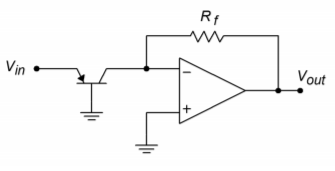
Figure \(\PageIndex{3}\): Basic antilog circuit.
The same comments about stability and signal limits apply to both the anti-log amplifier and the log amplifier. Also, there is one interesting observation worth remembering: in a general sense, the response of the op amp system echoes the characteristics of the elements used in the feedback network. When just resistors are used, which have a linear relation between voltage and current, the resulting amplifier exhibits a linear response. If a logarithmic PN junction is used, the result is an amplifier with a log or anti-log response.
Example \(\PageIndex{1}\)
Determine the output voltage for the circuit of Figure \(\PageIndex{1}\) if \(V_{in} = 1 V\), \(R_i = 50 k\Omega \), and \(I_s = 30 nA\). Assume \(T = 300\) Kelvin. Also determine the output for inputs of 0.5 V and 2 V.
For \(V_{in} = 1 V\)
\[ V_{out} = −0.0259 \ln \frac{V_{in}}{R_i I_s} \nonumber \]
\[ V_{out} = −0.0259 \ln \frac{1 V}{50 k 30 nA} \nonumber \]
\[ V_{out} = −0.0259 \ln 666.6 \nonumber \]
\[ V_{out} = −0.1684 V \nonumber \]
For \(V_{in} = 0.5 V\)
\[ V_{out} = −0.0259 \ln \frac{.5 V}{50 k 30 nA} \nonumber \]
\[ V_{out} = −0.0259 \ln 333.3 \nonumber \]
\[ V_{out} = −0.1504 V \nonumber \]
For \(V_{in} = 2 V\)
\[ V_{out} = −0.0259 \ln \frac{2 V}{50 k 30 nA} \nonumber \]
\[ V_{out} = −0.0259 \ln 1333 \nonumber \]
\[ V_{out} = −0.1864 V \nonumber \]
Notice that for each doubling of the input signal, the output signal went up a constant 18 mV. Such is the nature of a log amplifier.
As noted, the basic log/anti-log forms presented have their share of problems. It is possible to create more elaborate and accurate designs, but generally, circuit design of this type is not for the faint-hearted, as the device-matching and temperature-tracking considerations are not minor.
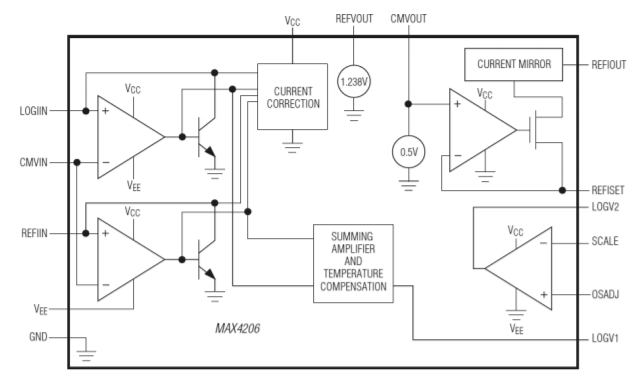
Figure \(\PageIndex{4}\): MAX4206 equivalent circuit. Reprinted courtesy of Maxim Integrated
Some manufacturers supply relatively simple-to-use log circuits in IC form. This takes much of the “grind” out of log circuit design. An example device is the MAX4206 from Maxim. An equivalent circuit for the MAX4206 is shown in Figure \(\PageIndex{4}\). An uncommitted amplifier and a voltage reference round out the package. The MAX4206 can be powered from single or bipolar supplies and operates over a five decade range. Further details on the design and application of higher quality log amplifiers may be found in Section 7.7: Extended Topic.
7.6.1: Four-Quadrant Multiplier
A four-quadrant multiplier is a device with two inputs and a single output. The output potential is the product of the two inputs along with a scaling factor, \(K\).
\[ V_{out} = K V_x V_y \label{7.14} \]
Typically, K is 0.1 in order to minimize the possibility of output overload. The schematic symbol for the multiplier is shown in Figure \(\PageIndex{5}\). It is called a fourquadrant device, as both inputs and the output may be positive or negative. An example device is the Analog Devices AD834. The AD834 operates from DC through 500 MHz and can be powered by supplies from \(\pm\)4 V through \(\pm\)15 V. Although multipliers are not really “non-linear” in and of themselves, they can be used in a variety of out-of-the-ordinary applications and in areas where log amps might be used.
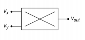
Figure \(\PageIndex{5}\): Schematic symbol for multiplier.
Multipliers have many uses including squaring, dividing, balanced modulation/demodulation, frequency modulation, amplitude modulation, and automatic gain control. The most basic operation, multiplication, involves using one input as the signal input and the other input as the gain control potential. Unlike the simple VCA circuit discussed earlier, this gain control potential is allowed to swing both positive and negative. A negative polarity will produce an inverted output. This basic connection is shown in Figure \(\PageIndex{6}\). This same circuit can be used as a balanced modulator. This is very useful for creating dual sideband signals for communications work. Multiplier ICs may have external connections for scale factor and offset adjust potentiometers. Also, they may be modeled as current sources, so an external op amp connected as a current-to-voltage converter may be required.
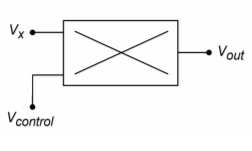
Figure \(\PageIndex{6}\): Multiplication circuit.
If the two inputs are tied together and fed from a single input, the result will be a squaring circuit. Squaring circuits can be very useful for RMS calculations and for frequency doubling. An example is shown in Figure \(\PageIndex{7}\).
The multiplier may also be used for division or square root functions. A divider circuit is shown in Figure \(\PageIndex{8}\). Here's how it works: First, note that the output of the multiplier, \(V_m\), is a function of \(V_x\) and the output of the op amp, \(V_{out}\).
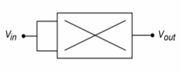
Figure \(\PageIndex{7}\): Squaring circuit.
\[ V_m = K V_x V_{out} \label{7.15} \]
\(V_m\) produces a current through \(R_2\). Note that the bottom end of \(R_2\) is at a virtual ground, so that all of \(V_m\) drops across \(R_2\).
\[ I_2 = \frac{V_m}{R_2} \nonumber \]
As we have already seen,
\[ I_1 = \frac{V_{in}}{R_1} \nonumber \]
Now, because the current into the op amp is assumed to be zero, \(I_1\) and \(I_2\) must be equal and opposite. It is apparent that the arbitrary direction of \(I_2\) is negative. Therefore, if \(R_1\) is set equal to \(R_2\),
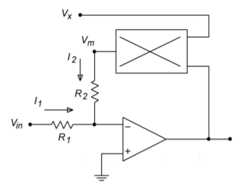
Figure \(\PageIndex{8}\): Divider circuit.
\[ V_m = −V_{in} \text{ and using Equation \ref{7.15}} \nonumber \]
\[ −V_{in} = K V_x V_{out} \nonumber \]
\[ V out = − \frac{V_{in}}{K V_x} \nonumber \]
\(V_x\) then sets the magnitude of the division. There are definite size restrictions on \(V_x\). If it is too small, output saturation will result. In a similar vein, if \(V_x\) is also tied back to the op amp's output, a square root function will result. Picking up the derivation at the next-to-last step,
\[ − V_{in} = K V_{out} V_{out} \nonumber \]
\[ V_{out} = \sqrt{\frac{−V_{in}}{K}} \label{7.17} \]
Example \(\PageIndex{2}\)
Determine the output voltage in Figure \(\PageIndex{7}\) if \(K = 0.1\) and the input signal is \(2 \sin 2 \pi 60 t\).
\[ V_{out} = K V_x V_y \nonumber \]
Because both inputs are tied together, this reduces to
\[ V_{out} = K V_{in}^{2} \nonumber \]
\[ V_{out} = 0.1(2 \sin 2 \pi 60 t)^{2} \label{7.18} \]
A basic trig identity is
\[ (\sin \omega)^{2} = 0.5−0.5 \cos 2 \omega \nonumber \]
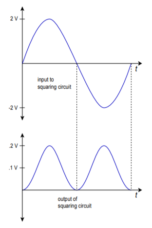
Figure \(\PageIndex{9}\): Waveforms of the squaring circuit of Example \(\PageIndex{2}\).
Substituting this into Equation \ref{7.18},
\[ V_{out} = 0.1(2−2 \cos 2 \pi 120 t) \nonumber \]
\[ V_{out} = 0.2−0.2 \cos 2 \pi 120 t \nonumber \]
This means that the output signal is 0.2 volts peak, and riding on a 0.2 volt DC offset. It also indicates a phase shift of -90 degrees and a doubling of the input frequency. This last attribute makes this connection very useful. We have seen many approaches to increasing a signal's amplitude, but this circuit allows us to increase its frequency. The waveforms are shown in Figure \(\PageIndex{9}\).