
9.2: Op Amp Oscillators
- Page ID
- 3601

9.2.1: Positive Feedback and the Barkhausen Criterion
In earlier work, we examined the concept of negative feedback. Here, a portion of the output signal is sent back to the input and summed out of phase with the input signal. The difference between the two signals then, is what is amplified. The result is stability in the circuit response because the large open-loop gain effectively forces the difference signal to be very small. Something quite different happens if the feedback signal is summed in phase with the input signal, as shown in Figure \(\PageIndex{1}\). In this case, the combined signal looks just like the output signal. As long as the open-loop gain of the amplifier is larger than the feedback factor, the signal can be constantly regenerated. This means that the signal source can be removed. In effect, the output of the circuit is used to create its own input. As long as power is maintained to the circuit, the output signal will continue practically forever. This self-perpetuating state is called oscillation. Oscillation will cease if the product of open loop gain and feedback factor falls below unity or if the feedback signal is not returned perfectly in phase (0\(^{\circ}\) or some integer multiple of 360\(^{\circ}\)). This combination of factors is called the Barkhausen Oscillation Criterion. We may state this as follows:
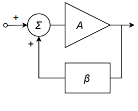
Figure \(\PageIndex{1}\): Positive feedback.
In order to maintain self-oscillation, the closed-loop gain must be unity or greater, and the loop phase must be \(N\) 360\(^{\circ}\), where \(N = 0, 1, 2, 3\dots\)
Note that when we examined linear amplifiers, we looked at this from the opposite end. Normally, you don't want amplifiers to oscillate, and thus you try to guarantee that the Barkhausen Criterion is never met by setting appropriate gain and phase margins.
A good example of positive feedback is the “squeal” sometimes heard from improperly adjusted public address systems. Basically, the microphone is constantly picking up the ambient room noise, which is then amplified and fed to the loudspeakers. If the amplifier gain is high enough or if the acoustic loss is low enough (i.e., the loudspeaker is physically close to the microphone), the signal that the microphone picks up from the loudspeaker can be greater than the ambient noise. The result is that the signal constantly grows in proper phase to maintain oscillation. The result is the familiar squealing sound. In order to stop the squeal, either the gain or the phase must be disrupted. Moving the microphone may change the relative phase, but it is usually easier to just reduce the volume a little. It is particularly interesting to listen to a system that is on the verge of oscillation. Either the gain or the phase is just not quite perfect, and the result is a rather irritating ringing sound, as the oscillation dies out after each word or phrase.
There are a couple of practical considerations to be aware of when designing oscillators. First of all, it is not necessary to provide a “start-up” signal source as seen in Figure \(\PageIndex{1}\). Normally, there is enough energy in either the input noise level or possibly in a turn-on transient to get the oscillator started. Both the turn-on transient and the noise signal are broad spectrum signals, so the desired oscillation frequency is contained within either of them. The oscillation signal will start to increase as time progresses due to the closed-loop gain being greater than one. Eventually, the signal will reach a point where further level increases are impossible due to amplifier clipping. For a more controlled, low-distortion oscillator, it is desirable to have the gain start to roll off before clipping occurs. In other words, the closed-loop gain should fall back to exactly one. Finally, in order to minimize frequency drift over time, the feedback network should be selective. Frequencies either above or below the target frequency should see greater attenuation than the target frequency. Generally, the more selective (i.e., higher \(Q\)) this network is, the more stable and accurate the oscillation frequency will be. One simple solution is to use an \(RLC\) tank circuit in the feedback network. Another possibility is to use a piezoelectric crystal. A block diagram of a practical oscillator is shown in Figure \(\PageIndex{2}\).
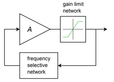
Figure \(\PageIndex{2}\): Practical oscillator
9.2.2: A Basic Oscillator
A real-world circuit that embodies all of the elements is shown in Figure \(\PageIndex{3}\). This circuit is not particularly efficient or cost-effective, but it does illustrate the important points. Remember, in order to maintain oscillation the closed-loop gain of the oscillator circuit must be greater than 1, and the loop phase must be a multiple of 360\(^{\circ}\).
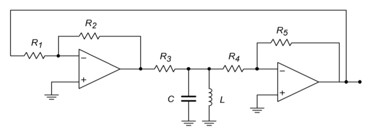
Figure \(\PageIndex{3}\): A basic oscillator.
To provide gain, a pair of inverting amplifiers is used. Note op amp 2 serves to buffer the output signal. As each stage produces a 180\(^{\circ}\) shift, the shift for the pair is 360\(^{\circ}\). The product of the gains has to be larger than the loss produced by the frequency selecting network. This network is made up of \(R_3\), \(L\), and \(C\). Because the \(LC\) combination produces an impedance peak at the resonant frequency, \(f_o\), a minimum loss will occur there. Also, at resonance, the circuit is basically resistive, so no phase change occurs. Consequently, this circuit should oscillate at the fo set by \(L\) and \(C\). This circuit can be easily tested in lab. For example, if you drop the gain of one of the op amp stages, there will not be enough system gain to over come the tank circuit's loss, and thus, oscillation will cease. You can also verify the phase requirement by replacing one of the inverting amplifiers with a noninverting amplifier of equal gain. The resulting loop phase of 180\(^{\circ}\) will halt oscillation. This circuit does not include any form of automatic gain adjustment, so the output signal may be clipped. If properly chosen, the slew rate of the op amp may be used as the limit factor. (A 741 will work acceptably for \(f_o\) in the low kHz range). Although this circuit does work and points out the specifics, it is certainly not a top choice for an oscillator design based on op amps.
9.2.3: Wien Bridge Oscillator
A relatively straightforward design useful for general-purpose work is the Wien bridge oscillator. This oscillator is far simpler than the generalized design shown in Figure \(\PageIndex{3}\), and offers very good performance. The frequency selecting network is a simple lead/lag circuit, such as that shown in Figure \(\PageIndex{4}\). This circuit is a frequency-sensitive voltage divider. It combines the response of both the simple lead and lag networks. Normally, both resistors are set to the same value. The same may be said for the two capacitors. At very low frequencies, the capacitive reactance is essentially infinite, and thus, the upper series capacitor appears as an open. Because of this, the output voltage is zero. Likewise, at very high frequencies the capacitive reactance approaches zero, and the lower shunt capacitor effectively shorts the output to ground. Again, the output voltage is zero. At some middle frequency the output voltage will be at a peak. This will be the preferred, or selected, frequency and will become the oscillation frequency so long as the proper phase relation is held. We need to determine the phase change at this point as well as the voltage divider ratio. These items are needed in order to guarantee that the Barkhausen conditions are met.
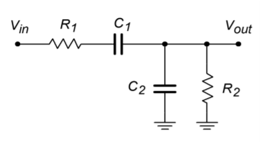
Figure \(\PageIndex{4}\): Lead/lag network.
First, note that
\[ \beta = \frac{Z_2}{Z_1+Z_2} \nonumber \]
where \(Z_1 = R_1 - jX_{C_1}\), and \(Z_2 = R_2 || -jX_{C_2}\).
\[ Z_2 = \frac{−j X_{C_2} R_2}{− j X_{C_2} + R_2} \nonumber \]
\[ Z_2 = \frac{− j X_{C_2} R_2}{− j X_{C_2} ( 1+ \frac{R_2}{− j X_{C_2}} )} \nonumber \]
\[ Z_2 = \frac{R_2}{1+ \frac{R_2}{− j X_{C_2}}} \nonumber \]
Recalling that \(X_C = 1/\omega C\), we find
\[ Z_1 = R_1− \frac{j}{\omega C_1} \nonumber \]
\[ Z_2 = \frac{R_2}{1+ j\omega R_2C_2} \nonumber \]
So,
\[ \beta = \frac{\frac{R_2}{1+ j\omega R_2 C_2}}{\frac{R_2}{1+ j \omega R_2 C_2} + R_1 − \frac{j}{\omega C_1}} \nonumber \]
\[ \beta = \frac{R_2}{R_2 + R_1 − \frac{j}{\omega C_1} + j \omega R_1 R_2 C_2 + \frac{R_2 C_2}{C_1}} \nonumber \]
\[ \beta = \frac{R_2}{R_2 \left(1+ \frac{C_2}{C_1}\right) + R_1+ j\left( \omega R_1 R_2 C_2− \frac{1}{\omega C_1} \right)} \label{9.1} \]
We can determine the desired frequency from the imaginary portion of Equation \ref{9.1}.
\[ \omega R_1 R_2 C_2 = \frac{1}{\omega C_1} \nonumber \]
\[ \omega ^2 = \frac{1}{R_1 R_2 C_1 C_2} \nonumber \]
\[ \omega = \frac{1}{\sqrt{R_1 R_2 C_1 C_2}} \label{9.2} \]
Normally, \(C_1 = C_2\) and \(R_1 = R_2\), so Equation \ref{9.2} reduces to
\[ \omega = \frac{1}{RC} \text{ or,} \nonumber \]
\[ f_o = \frac{1}{2 \pi RC} \label{9.3} \]
To find the magnitude of the feedback factor, and thus the required forward gain of the op amp, we need to examine the real portion of Equation \ref{9.1}.
\[ \beta = \frac{R_2}{R_2 \left( 1+ \frac{C_2}{C_1} \right) +R1} \nonumber \]
Assuming that equal components are used, this reduces to
\[ \beta = \frac{R}{3R} \text{ or simply,} \nonumber \]
\[ \beta = \frac{1}{3} \nonumber \]
The end result is that the forward gain of the amplifier must have a gain of slightly over 3 and a phase of 0\(^{\circ}\) in order to maintain oscillation. It also means that the frequency of oscillation is fairly easy to set and can even be adjusted if potentiometers are used to replace the two resistors. The final circuit is shown in Figure \(\PageIndex{5}\).
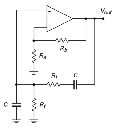
Figure \(\PageIndex{5}\): Wien bridge oscillator.
This circuit uses a combination of negative feedback and positive feedback to achieve oscillation. The positive feedback loop utilizes \(R_t\) and \(C\). The negative feedback loop utilizes \(R_a\) and \(R_b\). \(R_b\) must be approximately twice the size of \(R_a\). If it is smaller, the \(A\beta \) product will be less than unity and oscillation cannot be maintained. If the gain is significantly larger, excessive distortion may result. Indeed, some form of gain reduction at higher output voltages is desired for this circuit. One possibility is to replace \(R_a\) with a lamp. As the signal amplitude increases across the lamp, its resistance increases, thus decreasing gain. At a certain point the lamp's resistance will be just enough to produce an \(A\beta \) product of exactly 1. Another technique is shown in Figure \(\PageIndex{6}\). Here an opposite approach is taken. Resistor \(R_b\) is first broken into two parts, the smaller part, \(R_{b2}\), is shunted by a pair of signal diodes. For lower amplitudes, the diodes are off and do not affect the circuit operation. At higher amplitudes, the diodes start to turn on, and thus start to short \(R_{b2}\). If correctly implemented, this action is not instantaneous and does not produce clipping. It simply serves to reduce the gain at higher amplitudes.
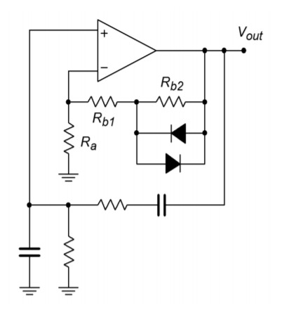
Figure \(\PageIndex{6}\): Wien bridge oscillator with gain adjustment.
Another way of drawing the Wien bridge oscillator is shown in Figure \(\PageIndex{7}\). This form clearly shows the Wien bridge configuration. Note that the output of the bridge is the differential input voltage (i.e., error voltage). In operation, the bridge is balanced, and thus, the error voltage is zero.
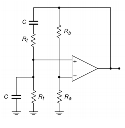
Figure \(\PageIndex{7}\): Wien bridge oscillator redrawn.
Example \(\PageIndex{1}\)
Determine the frequency of oscillation for the circuit of Figure \(\PageIndex{8}\).
\[ f_o = \frac{1}{2 \pi RC} \nonumber \]
\[ f_o = \frac{1}{2 \pi \times 50 k\times .01 \mu F} \nonumber \]
\[ f_o = 318Hz \nonumber \]
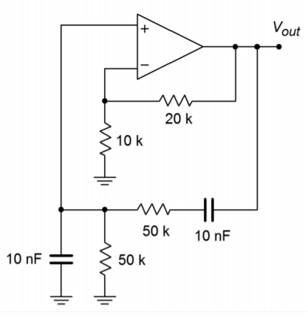
Figure \(\PageIndex{8}\): Oscillator for Example \(\PageIndex{1}\).
For other frequencies, either \(R\) or \(C\) may be altered as required. Also, note that the forward gain works out to exactly 3, thus perfectly compensating the positive feedback factor of 1/3. In reality, component tolerances make this circuit impractical. To overcome this difficulty, a small resistor/diode combination may be placed in series with the 20 k\(\Omega\), as shown in Figure \(\PageIndex{6}\). A typical resistor value would be about one-fourth to one-half the value of \(R_f\), or about 5 k\(\Omega\) to 10 k\(\Omega\) in this example. \(R_f\) would be decreased slightly as well (or, \(R_i\) might be increased).
The ultimate accuracy of \(f_o\) depends on the tolerances of \(R\) and \(C\). If 10% parts are used in production, a variance of about 20% is possible. Also, at higher frequencies, the op amp circuit will produce a moderate phase shift of its own. Thus, the assumption of a perfect noninverting amplifier is no longer valid, and some error in the output frequency will result. With extreme values in the positive feedback network, it is also possible that some shift of the output frequency may occur due to the capacitive and resistive loading effects of the op amp. Normally, this type of loading is not a problem, as the op amp's input resistance is very high, and its input capacitance is quite low.
Example \(\PageIndex{2}\)
Figure \(\PageIndex{9}\) shows an adjustable oscillator. Three sets of capacitors are used to change the frequency range, whereas a dual-gang potentiometer is used to adjust the frequency within a given range. Determine the maximum and minimum frequency of oscillation within each range.
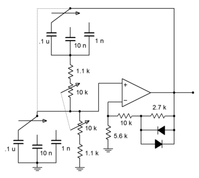
Figure \(\PageIndex{9}\): Adjustable oscillator.
First, note that the capacitors are spaced by decades. This means that the resulting frequency ranges will also change by factors of 10. The 0.1 \(\mu\)F capacitor will produce the lowest range, the 10 nF will produce a range 10 times higher, and the 1 nF range will be 10 times higher still. Thus, we only need to calculate the range produced by the 0.1 \(\mu\)F.
The maximum frequency of oscillation within a given range will occur with the lowest possible resistance. The minimum resistance is seen when the 10 k\(\Omega\) pot is fully shorted, the result being 1.1 k\(\Omega\). Conversely, the minimum frequency will occur with the largest resistance. When the pot is fully in the circuit, the resulting sum is 11.1 k\(\Omega\). Note that a dual-gang potentiometer means that both units are connected to a common shaft; thus, both pots track in tandem.
For \(f_{minimum}\) with 0.1\(\mu\)F:
\[ f_o = \frac{1}{2 \pi RC} \nonumber \]
\[ f_o = \frac{1}{2 \pi \times 11.1 k\times 0.1 \mu F} \nonumber \]
\[f_o = 143.4 Hz \nonumber \]
For \(f_{maximum}\) with 0.1 \(\mu\)F:
\[ f_o = \frac{1}{2 \pi RC} \nonumber \]
\[ f_o = \frac{1}{2 \pi \times 1.1 k\times 0.1 \mu F} \nonumber \]
\[ f_o = 1.447 kHz \nonumber \]
For the 0.01 \(\mu\)F, the ranges would be 1.434 kHz to 14.47 kHz, and for the 0.001 \(\mu\)F, the ranges would be 14.34 kHz to 144.7 kHz. Note that each range picks up where the previous one left off. In this way, there are no “gaps”, or unobtainable frequencies. For stable oscillation, this circuit must have a gain of 3. For low-level outputs, the diodes will not be active, and the forward gain will be
\[ A_v = 1+ \frac{R_f}{R_i} \nonumber \]
\[ A_v = 1+ \frac{10 k+2.7 k}{5.6 k} \nonumber \]
\[ A_v = 3.27 \nonumber \]
As the signal rises, the diodes begin to turn on, thus shunting the 2.2 k\(\Omega\) resistor and dropping the gain back to exactly 3.
9.2.4: Phase Shift Oscillator
Considering the Barkhausen Criterion, it should be possible to create an oscillator by using a simple phase shift network in the feedback path. For example, if the circuit uses an inverting amplifier (-180\(^{\circ}\) shift), a feedback network with an additional 180\(^{\circ}\) shift should create oscillation.
The only other requirement is that the gain of the inverting amplifier be greater than the loss produced by the feedback network. This is illustrated in Figure \(\PageIndex{10}\). The feedback network can be as simple as three cascaded lead networks. The lead networks will produce a combined phase shift of 180\(^{\circ}\) at only one frequency. This will become the frequency of oscillation. In general, the feedback network will look something like the circuit of Figure \(\PageIndex{11}\). This form of \(RC\) layout is usually referred to as a ladder network.
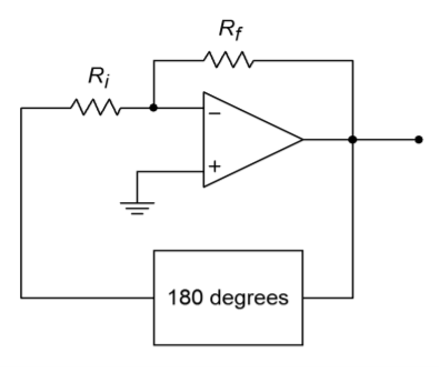
Figure \(\PageIndex{10}\): Block diagram of phase shift oscillator.
There are many ways in which \(R\) and \(C\) may be set in order to create the desired 180\(^{\circ}\) shift. Perhaps the most obvious scheme is to set each stage for a 60\(^{\circ}\) shift. The components are determined by finding a combination that produces a 60\(^{\circ}\) shift at the desired frequency. In order to avoid loading effects, each stage must be set to higher and higher impedances. For example, \(R_2\) might be set to 10 times the value of \(R_1\), and \(R_3\) set to 10 times the value of \(R_2\). The capacitors would see a corresponding decrease. Because the tangent of the phase shift yields the ratio of \(X_C\) to \(R\), at our desired 60\(^{\circ}\) we find
\[ \tan 60 = \frac{X_C}{R} \nonumber \]
\[ 1.732 = \frac{X_C}{R} \nonumber \]
\[ X_C = 1.732 R \nonumber \]
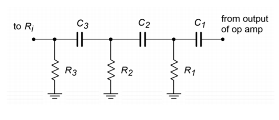
Figure \(\PageIndex{11}\): Phase shift network
Using this in the general reactance formula produces
\[ f_o = \frac{1}{2 \pi 1.732 RC} \label{9.4} \]
Likewise, a look at the magnitude shows the approximate loss per stage of
\[ \beta = \frac{R}{\sqrt{R^2 + X_C^{2}}} \nonumber \]
\[ \beta = \frac{R}{\sqrt{R^2 +(1.732 R)^{2}}} \nonumber \]
\[ \beta = .5 \nonumber \]
Because there are three stages, the total loss for the feedback network would be 0.125. Therefore, the inverting amplifier needs a gain of 8 in order to set the \(A\beta \) product to unity. Remember, these results are approximate and depend on minimum interstage loading. A more exacting analysis will follow shortly.
Example \(\PageIndex{3}\)
Determine the frequency of oscillation in Figure \(\PageIndex{12}\).
\[ f_o = \frac{1}{2 \pi 1.732 RC} \nonumber \]
\[ f_o = \frac{1}{2 \pi \times 1.732\times 1 k\times 100 nF} \nonumber \]
\[ f_o = 919 Hz \nonumber \]
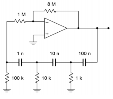
Figure \(\PageIndex{12}\): Phase shift oscillator (minimum loading form).
Figure \(\PageIndex{12}\) graphically points up the major problem with the “60\(^{\circ}\) per stage” concept. In order to prevent loading, the final resistors must be very high. In this case a feedback resistor of 8 M\(\Omega\) is required. It is possible to simplify the circuit somewhat by omitting the 1 M\(\Omega\) and connecting the 100 k\(\Omega\) directly to the op amp as shown in Figure \(\PageIndex{13}\). This saves one part and does allow the feedback resistor to be dropped in value, but the resulting component spread is still not ideal.
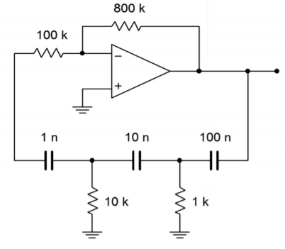
Figure \(\PageIndex{13}\): Improved phase shift oscillator.
If we accept the loading effect, we can simplify things a bit by making each resistor and capacitor the same size, as shown in Figure \(\PageIndex{14}\). With these values, we can be assured that the resulting frequency will no longer be 919 Hz, as Equation \ref{9.4} is no longer valid. Also, it is quite likely that the loss produced by the network will no longer be 0.125.
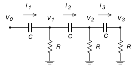
Figure \(\PageIndex{14}\): Phase shift analysis.
We need to determine the general input/output \((V_0 / V_3)\) ratio of the ladder network, and from this, find the gain and frequency relations for a net phase shift of -180\(^{\circ}\). One technique involves the use of simultaneous loop equations. Because all resistors and capacitors are equal in this variation, we will be able to simplify our equations readily. By inspection, the three loop equations are (from left to right):
\[ V_0 = (R+ X_C) I_1 − R I_2 \label{9.5} \]
\[ 0 = −R I_1 + (2 R + X_C) I_2 − R I_3 \label{9.6} \]
\[ 0 = −R I_2 + (2 R + X_C) I_3 \label{9.7} \]
Also, note that
\[ V_3 = I_3 R \label{9.8} \]
We now have expressions for \(V_0\) and \(V_3\), however, \(V_0\) is in terms of \(I_1\) and \(I_2\), and \(V_3\) is in terms of \(I_3\). Write \(I_1\) and \(I_2\) in terms of \(I_3\) so that we can substitute these back into Equation \ref{9.5}. Rewriting Equation \ref{9.7} yields an expression for \(I_2\)
\[ I_2 = I_3 \left(2+ \frac{X_C}{R}\right) \label{9.9} \]
For \(I_1\), rewrite Equation \ref{9.6}
\[ I_1 = \left( 2+ \frac{X_C}{R} \right) I_2 − I_3 \label{9.10} \]
Substituting Equation \ref{9.9} into Equation \ref{9.10} yields
\[ I_1 = I_3 \left(\left( 2+ \frac{X_C}{R} \right)^{2} −1\right) \label{9.11} \]
Thus, \(V_0\) may be rewritten as
\[ V_0 = I_3 (R+ X_C) \left( \left( 2 + \frac{X_C}{R} \right)^2 −1 \right)− I_3 R \left( 2+ \frac{X_C}{R} \right) \label{9.12} \]
Equation \ref{9.12} may be simplified to
\[ V_0 = I_3 \left( R \left( 2 + \frac{X_C}{R} \right)^2 + X_C \left( 2+ \frac{X_C}{R} \right)^2 −3 R−2 X_C \right) \label{9.13} \]
The input/output expression is simplified as follows.
\[ \frac{V_0}{V_3} = \left( R \left( 2+ \frac{X_C}{R} \right)^2 + X_C \left( 2+ \frac{X_C}{R} \right)^2 −3 R −2 X_C \right) \left( \frac{1}{R} \right) \label{9.14} \]
\[ \frac{V_0}{V_3} = \left(2+ \frac{X_C}{R} \right)^2 + \frac{X_C}{R} \left(2+ X C R \right)^2 − 3 − 2 \frac{X_C}{R} \nonumber \]
\[ \frac{V_0}{V_3} = 1+ \frac{6 X_C}{R} + 5 \frac{X_C^2}{R^2} + \frac{X_C^3}{R^3} \label{9.15} \]
At this point, we are nearly done with the general equation. All that is left is to substitute \(1 / j\omega C\) in place of \(X_C\). Remember, \(j^2 = -1\)
\[ \frac{V_0}{V_3} = 1+ \frac{6}{j\omega C R} − \frac{5}{\omega ^2 C^2 R^2} − \frac{1}{j \omega ^3 C^3 R^3} \label{9.16} \]
This Equation contains both real and imaginary terms. For this Equation to be satisfied, the imaginary components \((6 / j\omega CR\) and \(1 / j\omega ^3 C^3 R^3 )\) must sum to zero, and the real components must similarly sum to zero (as there are only two terms, their magnitudes must be equal). We can use these facts to find both the gain and the frequency.
\[ \frac{6}{j\omega CR} = \frac{1}{j \omega ^3 C^3 R^3} \nonumber \]
\[ \frac{1}{j\omega CR} = \frac{1}{ 6 j \omega ^3 C^3 R^3} \nonumber \]
\[1 = \frac{1}{ 6 j \omega ^2 C^2 R^2} \nonumber \]
\[ \omega ^2 = \frac{1}{ 6 C^2 R^2} \label{9.17} \]
\[ \omega = \frac{1}{\sqrt{6}CR} \ or, \label{9.18} \]
\[ f_o = \frac{1}{2 \pi \sqrt{6}CR} \label{9.19} \]
For the gain, we solve Equation \ref{9.16} in terms of the voltage ratio and zero the imaginary terms, because the result must be real.
\[ \frac{V_0}{V_3} = 1 − \frac{5}{\omega ^2 C^2 R^2} \label{9.20} \]
Substituting Equation \ref{9.17} into Equation \ref{9.20} yields
\[ \frac{V_0}{V_3} = 1 − \frac{5}{\frac{1}{6 C^2 R^2} C^2 R^2} \label{9.21} \]
\[ \frac{V_0}{V_3} =1 −5\times 6 \nonumber \]
\[ \frac{V_0}{V_3} =−29 \label{9.22} \]
The gain of the ladder network is \(V_3 /V_0\), or the reciprocal of Equation \ref{9.22}, or
\[ \beta = \frac{1}{−29} \label{9.23} \]
The loss produced will be 1/29. This has the disadvantage of requiring a forward gain of 29 instead of 8 (as in the previous form). This disadvantage is minor compared to the advantage of reasonable component values.
Example \(\PageIndex{4}\)
Determine a value for \(R_f\) in Figure \(\PageIndex{15}\) in order to maintain oscillation. Also determine the oscillation frequency.
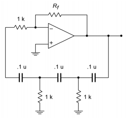
Figure \(\PageIndex{15}\): Equal component phase shift oscillator.
Equation \ref{9.23} shows that the inverting amplifier must have a gain of 29.
\[ A_v = − \frac{R_f}{R_i} \nonumber \]
\[ R_f = − \frac{R_i}{A_v} \nonumber \]
\[ R_f = −1 k \times −29 \nonumber \]
\[ R_f = 29 k \nonumber \]
Of course, the higher standard value will be used. Also, in order to control the gain at higher levels, a diode/resistor combination (as used in the Wien bridge circuits) should be placed in series with \(R_f\). Without a gain limiting circuit, excessive distortion may occur.
\[ f_o = \frac{1}{2\pi \sqrt{6} RC} \nonumber \]
\[ f_o = \frac{1}{2 \pi \sqrt{6}\times 1k\times 0.1\mu F} \nonumber \]
\[ f_o = 650 Hz \nonumber \]
Computer Simulation
In order to verify Equations \ref{9.3} and \ref{9.19}, the gain and phase responses of the feedback networks of Figures \(\PageIndex{13}\) and \(\PageIndex{15}\) are found in Figure \(\PageIndex{16}\). These graphs were obtained via the standard Multisim route. Note that the phase for both circuits hits -180\(^{\circ}\) very close to the predicted frequencies. The equal value network prediction is very accurate, whereas the staggered network prediction is off by only a few percent. Once the phase exceeds -180\(^{\circ}\), the Multisim grapher wraps it back to +180\(^{\circ}\), so it is very easy to see this frequency. Likewise, the gain response agrees with the derivations for attenuation at the oscillation frequency. It can be very instructive to analyze these circuits for the gain and phase response at each stage as well.
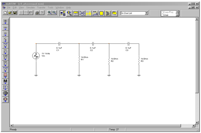
Figure \(\PageIndex{16a}\): Equal value network in Multisim.
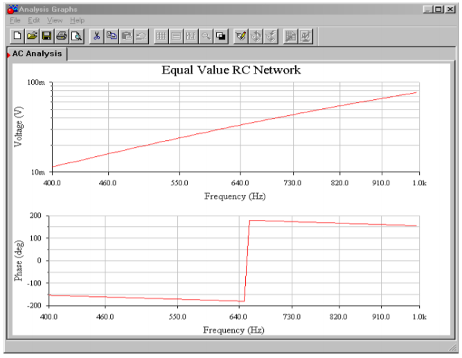
Figure \(\PageIndex{16b}\): Response of equal value network.
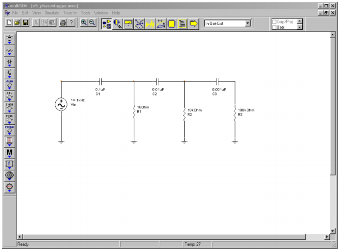
Figure \(\PageIndex{16c}\): Staggered value network in Multisim.
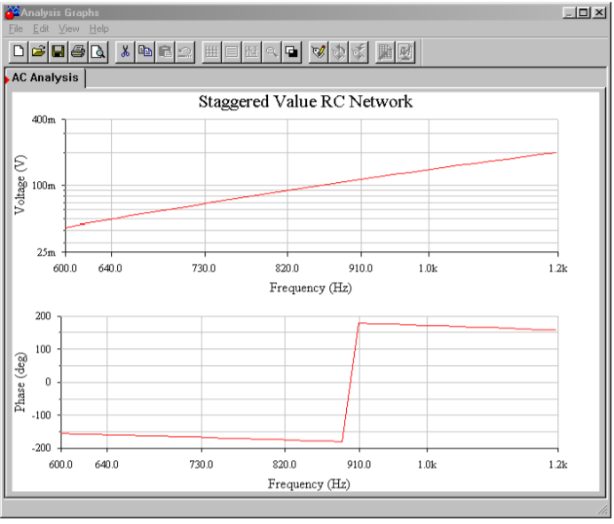
Figure \(\PageIndex{16d}\): Response of staggered value network.
9.2.5: Square/Triangle Function Generator
Besides generating sine waves, op amp circuits may be employed to generate other wave shapes such as ramps, triangle waves, or pulses. Generally speaking, squareand pulse-type waveforms may be derived from other sources through the use of a comparator. For example, a square wave may be derived from a sine wave by passing it through a comparator, such as those seen in Chapter Seven. Linear waveforms such as triangles and ramps may be derived from the charge/discharge action of a capacitor. As you may recall from basic circuit theory, the voltage across a capacitor will rise linearly if it is driven by a constant current source. One way of achieving this linear rise is with the circuit of Figure \(\PageIndex{17}\).
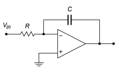
Figure \(\PageIndex{17}\): Ramp generator.
In essence, this circuit is an inverting amplifier with a capacitor taking the place of \(R_f\). The input resistor, \(R\), turns the applied input voltage into a current. Because the current into the op amp itself is negligible, this current flows directly into capacitor \(C\). As in a normal inverting amplifier, the output voltage is equal to the voltage across the feedback element, though inverted. The relationship between the capacitor current and voltage is
\[ \frac{d_v}{d_t} = \frac{i}{C} \label{9.24} \]
\[ V(t) = \frac{1}{C} \int i dt \nonumber \]
\[ V_{out} = − \frac{1}{C} \int i dt \label{9.25} \]
As expected, a fast rise can be created by either a small capacitor or a large current. (As a side note, this circuit is called an integrator and will be examined in greater detail in the next chapter.)
By choosing appropriate values for \(R\) and \(C\), the \(V_{out}\) ramp may be set at a desired rate. The polarity of the ramp's slope is determined by the direction of the input current; a positive source will produce a negative going ramp and vice versa. If the polarity of the input changes at a certain rate, the output ramp will change direction in tandem. The net effect is a triangle wave. A simple way to generate the alternating input polarity is to drive \(R\) with a square wave. As the square wave changes from plus to minus, the ramp changes direction. This is shown in Figure \(\PageIndex{18}\).
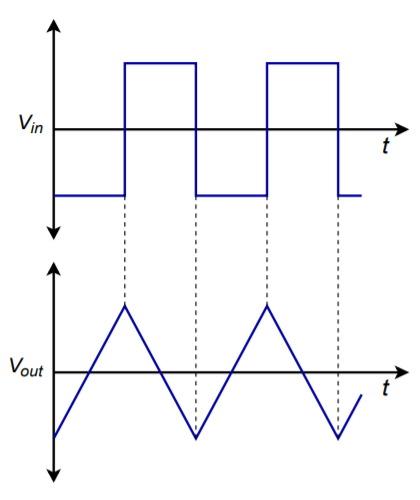
Figure \(\PageIndex{18}\): Ramp generator waveforms.
So, we are now able to generate a triangle wave. The only problem is that a square wave source is needed. How do we produce the square source? As mentioned earlier, a square wave may be derived by passing an AC signal through a comparator. Logically then, we should be able to pass the output triangle wave into a comparator in order to create the needed square wave. The resulting circuit is shown in Figure \(\PageIndex{19}\). A comparator with hysteresis is used to turn the triangle into a square wave. The square then drives the ramp circuit. The circuit produces two simultaneous outputs: a square wave that swings to \(\pm\) saturation and a triangle wave that swings to the upper and lower comparator thresholds. This is shown in Figure \(\PageIndex{20}\). The thresholds may be determined from the equations presented in Chapter Seven. In order to determine the output frequency, the V/s rate of the ramp is determined from Equation \ref{9.24}. Knowing the peak-to-peak swing of the triangle is \(V_{\text{upper thres}} - V_{\text{lower thres}}\), the period of the wave may be found. The output frequency is the reciprocal of the period.
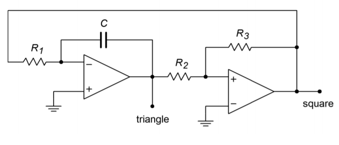
Figure \(\PageIndex{19}\): Triangle/square generator.
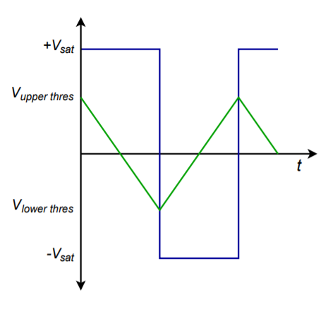
Figure \(\PageIndex{20}\): Output waveforms of triangle/square generator.
Example \(\PageIndex{5}\)
Determine the output frequency and amplitudes for the circuit of Figure \(\PageIndex{21}\). Use \(V_{sat} = \pm 13 V\).
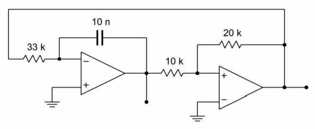
Figure \(\PageIndex{21}\): Signal generator for Example \(\PageIndex{5}\).
First, note that the comparator always swings between \(+V_{sat}\) and \(-V_{sat}\). Now, determine the upper and lower thresholds for the comparator.
\[ V_{\text{upper thres}} = V_{sat} \frac{R_2}{R_3} \nonumber \]
\[ V_{\text{upper thres}} = 13 V \frac{10 k}{20 k} \nonumber \]
\[ V_{\text{upper thres}} = 6.5 V \nonumber \]
The lower threshold will be -6.5 V. We now know that the triangle wave output will be 13 V peak-to-peak. From this we may determine the output period.
Because the ramp generator is driven by a square wave with an amplitude of \(V_{sat}\), Equation \ref{9.24} may be rewritten as
\[ \frac{d_v}{d_t} = \frac{V_{sat}}{RC} \nonumber \]
\[ \frac{d_v}{d_t} = \frac{13V}{33 k\times 0.01 \mu F} \nonumber \]
\[ \frac{d_v}{d_t} = 39,394V/s \nonumber \]
The time required to produce the 13 V peak-to-peak swing is
\[ T = \frac{13 V}{39,394 V/s} \nonumber \]
\[ T = 330 \mu s \nonumber \]
This represents one half-cycle of the output wave. To go from +6.5 V to -6.5 V and back will require 660 \(\mu\)s. Therefore, the output frequency is
\[ f = \frac{1}{T} \nonumber \]
\[ f = \frac{1}{660 \mu s} \nonumber \]
\[ f = 1.52 kHz \nonumber \]
The resulting frequency of Example \(\PageIndex{5}\) may be adjusted by changing either the 33 k\(\Omega\) resistor or the 10 nF capacitor. Changing the comparator's resistors can alter the thresholds, and thus alter the frequency, but this is generally not recommended, as a change in output amplitude will occur as well. By combining steps, the above process may be reduced to a single equation:
\[ f = \frac{1}{\frac{2V_{pp}}{V_{sat}} RC} \label{9.26} \]
where \(V_{pp}\) is the difference between \(V_{upper thres}\) and \(V_{lower thres}\). Note that if \(R_3\) is 4 times larger than \(R_2\) in the comparator, Equation \ref{9.26} reduces to
\[ f = \frac{1}{RC} \nonumber \]
and the peak triangle wave amplitude is one-fourth of \(V_{sat}\).
Generally, circuits such as this are used for lower frequency work. For clean square waves, very fast op amps are required. Finally, for lower impedance loads, the outputs should be buffered with voltage followers.
Computer Simulation
The Multisim simulation for the signal generator of Example \(\PageIndex{5}\) is shown in Figure \(\PageIndex{22}\). The square and triangle outputs are plotted together so that the switching action can be seen. Note how each wave is derived form the other. The output plot is delayed 5 milliseconds in order to guarantee a plot of the steady state output. Failure to delay the plotting times will result in a graph of the initial turn-on transients. It may take many milliseconds before the waveforms finally stabilize, depending on the desired frequency of oscillation and the initial circuit conditions. Finally, note the sharp rising and falling edges of the square wave. This is due to the moderately fast slew rate of the LF411 op amp chosen. Had a slower device such as the 741 been used, the quality of the output waveforms would have suffered.
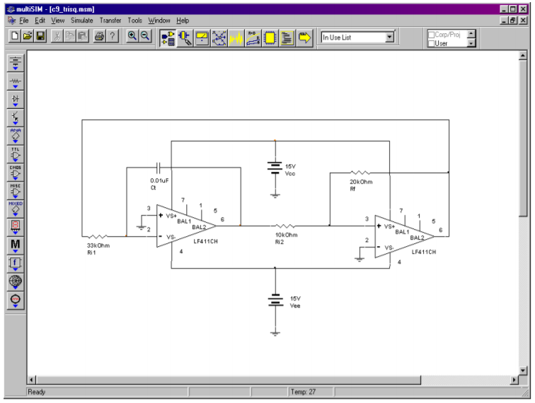
Figure \(\PageIndex{22a}\): Triangle/square generator in Multisim.
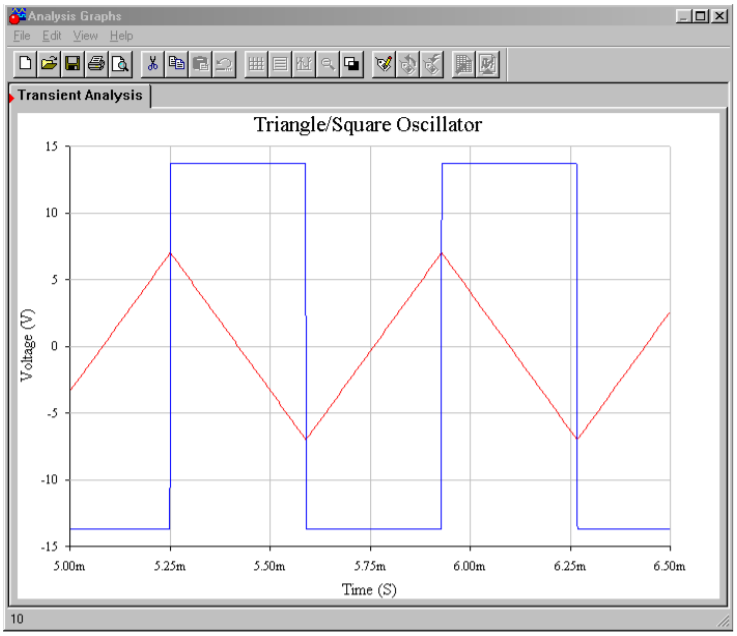
Figure \(\PageIndex{22b}\): Output waveforms from simulator.
If an accurate triangle wave is not needed, and only a square wave is required, the circuit of Figure \(\PageIndex{19}\) may be reduced to a single op amp stage. This is shown in Figure \(\PageIndex{23}\). This circuit is, in essence, a comparator. Resistors \(R_1\) and \(R_2\) form the positive feedback portion and set the effective comparator trip point, or threshold. The measurement signal is the voltage across the capacitor. The potentials of interest are shown in Figure \(\PageIndex{24}\). If the output is at positive saturation, the noninverting input will see a percentage of this, depending on the voltage divider produced by \(R_1\) and \(R_2\). This potential is \(V_{upper thres}\). Because the output is at positive saturation, the capacitor \(C\), will be charging towards it. Because it is charging through resistor \(R\), the waveform is an exponential type. Once the capacitor voltage reaches \(V_{upper thres}\), the noninverting input will no longer be greater than the inverting input, and the device will change to the negative state. At this point, \(C\) will reverse its course and move towards negative saturation. At the lower threshold, the op amp will again change state, and the process repeats. In order to determine the frequency of oscillation, we need to find how long it takes the capacitor to charge between the two threshold points. Normally the circuit will be powered from equal magnitude supplies, and therefore \(+V_{sat} = -V_{sat}\) and \(V_{upper thres} = V_{lower thres}\). By inspection,
\[ V_{thres} = V_{sat} \frac{R_1}{R_1+R_2} \label{9.27} \]
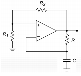
Figure \(\PageIndex{23}\): Simple square wave generator.
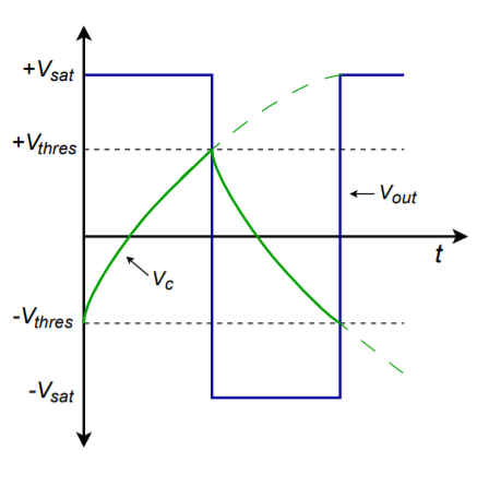
Figure \(\PageIndex{24}\): Waveforms of a simple square wave generator.
The capacitor voltage is
\[ V_C (t) = V_k (1 −\epsilon^{\frac{−t}{RC}}) \label{9.28} \]
where \(V_k\) is the total potential applied to the capacitor. Because the capacitor will start at one threshold and attempt to charge to the opposite saturation limit, this is
\[ V_k = V_{sat} + V_{thres} \label{9.29} \]
Combining Equation \ref{9.27}, Equation \ref{9.28}, and Equation \ref{9.29} yields
\[ V_C (t) = ( V_{sat} + V_{thres} )\left(1 −\epsilon^{\frac{−t}{RC}}\right) \label{9.30} \]
At the point where the comparator changes state,
\[ V_C = 2 V_{thres} \label{9.31} \]
Combining Equation \ref{9.30} and Equation \ref{9.31} produces
\[ 2 V_{thres} = (V_{sat} + V_{thres}) \left(1−\epsilon^{−t R C} \right) \\ 1−\epsilon^{\frac{−t}{RC}} = \frac{2 V_{thres}}{V_{sat} + V_{thres}} \\ 1−\epsilon^{\frac{−t}{RC}} = \frac{2 V_{sat} \frac{R_1}{R_1+ R_2}}{V_{sat}\left( 1+ \frac{R_1}{R_1+ R_2} \right)} \\ 1−\epsilon^{\frac{−t}{RC}} = \frac{2 R_1}{2 R_1+R_2} \\ \epsilon^{\frac{−t}{RC}} = \frac{R_2}{2 R_1+R_2} \\ \frac{−t}{RC} = \ln \left( \frac{R_2}{2 R_1+R_2} \right) \\ t = RC \ln \left( \frac{2 R_1+ R_2}{R_2} \right) \nonumber \]
This represents the charge time of the capacitor. One period requires two such traverses, so we may say
\[ T = 2 RC \ \ln \left( \frac{2 R_1+R_2}{R_2} \right) \ or, \nonumber \]
\[ f_o = \frac{1}{2 RC \ \ln \left( \frac{2 R_1+ R_2}{R_2} \right)} \label{9.32} \]
We can transform Equation \ref{9.32} into “nicer” forms by choosing values for \(R_1\) and \(R_2\) such that the log term turns into a convenient number, such as 1 or 0.5. For example, if we set \(R_1 = 0.859 R_2\), the log term is unity, and consequently Equation \ref{9.32} becomes \(f_o = 1 / 2RC\)
Example \(\PageIndex{6}\)
Design a 2 kHz square wave generator using the circuit of Figure \(\PageIndex{23}\). For convenience, set \(R_1 = 0.859 R_2\). If \(R_1\) is arbitrarily set to 10 k\(\Omega\), then
\[ R_1 = 0.859 R_2 \nonumber \]
\[ R_2 = \frac{R_1}{0.859} \nonumber \]
\[ R_2 = \frac{10 k}{0.859} \nonumber \]
\[ R_2 = 11.64 k \nonumber \]
In order to set the oscillation frequency, \(R\) is arbitrarily set to 10 k\(\Omega\), and \(C\) is then determined.
\[ f_o = \frac{1}{2 RC} \nonumber \]
\[ C = \frac{1}{2 R f_o} \nonumber \]
\[ C = \frac{1}{2\times 10 k\times 2 kHz} \nonumber \]
\[ C = 25 nF \nonumber \]
Computer Simulation
A simulation of the square wave generator of Example \(\PageIndex{6}\) is shown in Figure \(\PageIndex{25}\). In order to graphically illustrate the importance of the op amp having sufficient bandwidth and slew rate, the simulation is run twice, once using the moderately fast LF411 and a second time using the much slower 741.
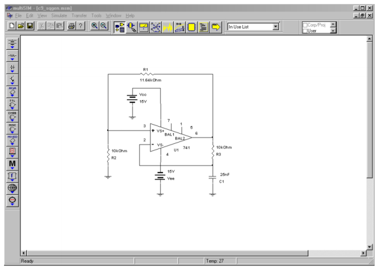
Figure \(\PageIndex{25a}\): Square wave generator in Multisim.
Both the output and capacitor voltages are plotted from the Transient Analysis. Using the LF411, the output waveform is very crisp with sharp rising and falling edges. The capacitor voltage appears exactly as it should. The resulting frequency is just a little lower than the 2 kHz target. In contrast, the 741 plots show some problems. First, the square wave has noticeable slew rate limiting on the transitions. Second, due to the slewing problems, the capacitor voltage waveshape appears distorted (note the excessive rounding of the peaks). These effects combine to produce a frequency about 15 percent lower than the target, or about 1.7 kHz. The end result is a lackluster output waveform.
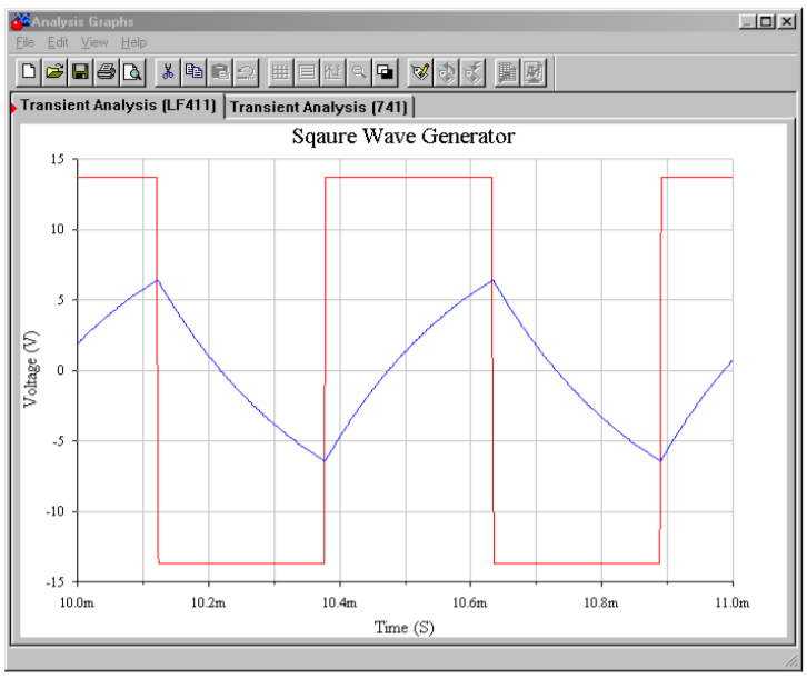
Figure \(\PageIndex{25b}\): Waveforms using LF411.
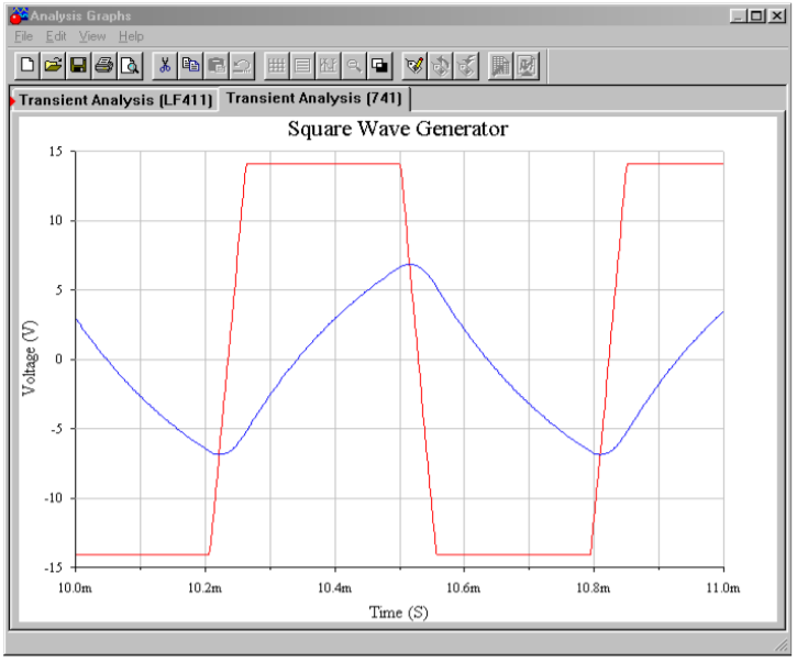
Figure \(\PageIndex{25c}\): Waveforms using 741.