
12.5: Analog-to-Digital Conversion
- Page ID
- 3625

Now that you know the basics behind digital-to-analog conversion, we may examine the converse system, analog-to-digital conversion. The analog-to-digital conversion process is sometimes referred to as quantization, implying the individual discrete steps that the output assumes. There are several techniques to produce the conversion. Some techniques are optimized for fastest possible conversion speed, and some for highest accuracy. We will investigate the more popular types.
The concept of AD conversion is simple enough: you wish to measure the voltage of the incoming waveform at specific instances in time. This measurement will be translated into a digital word. One practical limitation is the fact that the conversion circuitry may require a small amount of computation or translation time. For ultimate accuracy, then, it is important that the measured waveform not change during the conversion interval. To do this, specialized subcircuits called track-and-hold (or sample-and-hold) amplifiers are used. They are usually abbreviated as T/H or S/H. Their job is to capture an input potential and produce a steady output to feed to the AD converter. The T/H schematic symbol is shown in Figure \(\PageIndex{1}\). When the T/H logic is in track mode, the circuit acts as a simple buffer, so its output voltage equals its input. When the logic goes to the hold state, the output voltage locks at its present potential and stays there until the circuit is switched back to track mode. A representation of this operation is shown in Figure \(\PageIndex{2}\).
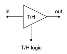
Figure \(\PageIndex{1}\): Symbol for the track-and-hold amplifier.
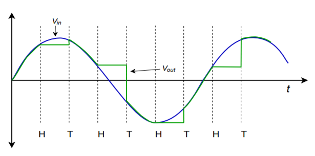
Figure \(\PageIndex{2}\): Track-and-hold operation.
In reality, the track-and-hold process is not perfect, and errors may arise. These errors are shown magnified in Figure \(\PageIndex{3}\). First of all, there is a small delay between the time the logic signal changes and the T/H starts to react. The exact amount of time is variable and is responsible for aperture error. This is equal to the voltage difference between the signals at the desired and actual times. Also, due to the dynamic nature of the process of switching from track to hold, some initial ringing may occur in the hold waveform.
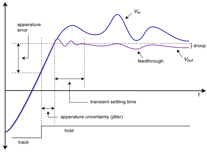
Figure \(\PageIndex{3}\): Track-and-hold errors.
You can see that as time progresses, the hold waveform tends to decay toward zero. This is because the held voltage is usually formed across a capacitor. Although the discharge time constant can be very long, it cannot be infinite, and thus, the charge eventually bleeds off. This parameter is measured by the droop rate (fundamental units of volts per second). Finally, the possibility of feedthrough error exists. If a large change occurs on the input waveform during the hold period, it is possible that a portion of the signal may “leak” through to the T/H output. These errors are particularly troublesome when working with high-resolution converters. Lower-resolution systems may not be adversely affected by these relatively small aberrations.
In order to create a T/H, a pair of high-impedance buffers are normally used, along with some form of switch element and a capacitor to hold the charge. Examples are shown in Figure \(\PageIndex{4}\). Figure \(\PageIndex{4a}\) shows the general voltage type, open-loop T/H. The buffers exhibit high input impedance. When the switch is closed, op amp 1 directly feeds op amp 2, and therefore the output voltage equals the input voltage. Normally, the hold capacitor is relatively small and does not adversely affect the drive capability of op amp 1.
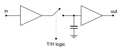
Figure \(\PageIndex{4a}\): Track-and-hold circuits. General open-loop voltage mode track-and-hold.
A more detailed version of this circuit is shown in Figure \(\PageIndex{4b}\). Each op amp is a FET input type for minimum input current draw. The switch is a simple JFET which is controlled by a comparator.
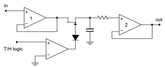
Figure \(\PageIndex{4b}\): Track-and-hold circuits. Op amp based track-and-hold.
When the T/H logic is high, the gate of the JFET is high, thus producing a low onresistance (i.e., a closed switch). When the comparator output goes low, the JFET is turned off creating a high impedance (i.e., open switch). In this state, op amp 2 is fed by the hold capacitor and buffers this potential to its output. For minimum droop, it is essential that the capacitor be a low leakage type and that op amp 2 have very low input bias current (e.g., FET input). The input resistor is used only to limit possible destructive discharge currents when the circuit is switched off. The diode positioned between the comparator and FET is used to prevent an excessively large positive comparator output potential from reaching the gate of the FET and possibly damaging it. (A comparator high will reverse-bias the series diode.) Figure \(\PageIndex{4c}\) shows an alternate circuit using a closed-loop, current-mode approach. Note that the hold capacitor is now forming part of an integrator. While the open-loop form offers faster acquisition and settling times, the closed-loop system offers improved signal tracking.
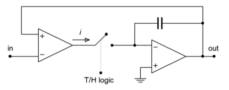
Figure \(\PageIndex{4c}\): Track-and-hold circuits. General closed-loop current mode track-and-hold.
A closed-loop voltage-mode is also possible, but the current form generally offers fewer problems with leakage and switching transients. For general-purpose work, a variety of track-and-hold amplifiers are available in IC form from several manufacturers.
Computer Simulation
A simulation of a track-and-hold circuit similar to the one shown in Figure \(\PageIndex{4b}\) is shown in Figure \(\PageIndex{5}\). The 100 Hz input signal is being sampled at 2 kHz, or 20 times per cycle.
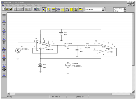
Figure \(\PageIndex{5a}\): Track and hold circuit in Multisim.
Three waveforms of interest are shown in the Transient Analysis graph. The input waveform is seen in the center as the smoothly varying sine wave. Along the bottom of the graph, narrow spikes can be seen. This is the T/H logic signal. The high portion of the pulse (at 0 volts) is the track logic, and the wider low signal (dropping below the −1 volt limit of the graph) represents the hold logic. The stair-stepped sine wave is the output voltage. Note how the circuit acquires or tracks the input signal during the track pulse and then remains at that level when the hold logic is applied. It is during these hold times that the computations will be performed by the analogto-digital converter.
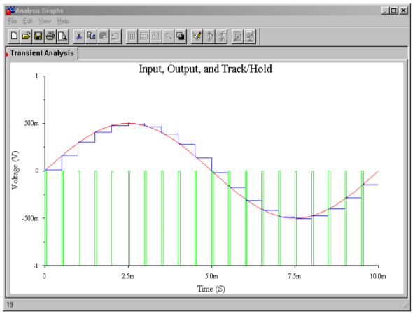
Figure \(\PageIndex{5b}\): Multisim waveforms for track-and-hold circuit.
12.5.1: Analog-to-Digital Conversion Techniques
Several different techniques have evolved for dealing with differing system requirements. These include flash, staircase, successive approximation, and delta-sigma forms.
Flash conversion is generally used for high-speed work, such as video applications. The circuits are usually low resolution. A flash converter is made up of a string of comparators as shown in Figure \(\PageIndex{6}\). The input signal is applied to all of the comparators simultaneously. Each comparator is also tied into a reference ladder. Effectively, there is one comparator for each quantization step. When a given signal is applied, a number of comparators towards the bottom of the string will produce a high level, as \(V_{in}\) will be greater than their references. Conversely, the comparators towards the top will indicate a low. The comparator at which the outputs shift from high to low indicates the step value closest to the input signal. The set of comparator outputs can be fed into a priority encoder that will turn this simple unweighted sequence into a normal binary word.
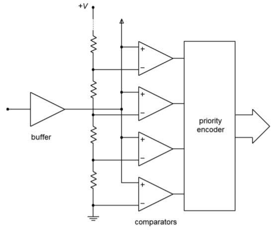
Figure \(\PageIndex{6}\): Flash converter.
The only time delay involved in the conversion is that of logic propagation delay. Therefore, this conversion technique is quite useful for rapidly changing signals. Its downfall lies in the fact that one comparator is needed for each possible output step change. An 8-bit flash converter requires 256 comparators, whereas a 16-bit version requires 65,536. Obviously, this is rather excessive, and units in the 4- to 6-bit range are common. Although 6-bit resolution may appear at first to be too coarse for any application, it is actually quite useful for video displays.
For high-resolution work, some other technique must be used. One possibility is shown in Figure \(\PageIndex{7}\). This is called a staircase converter. Its operation is fairly simple. When a conversion is first started, the output of the counter will be all zeros. This produces a DAC output of zero, and thus, the comparator output will be high. The next clock cycle will increment the up counter, causing the DAC output to increase by one step-level. This signal is compared against the input, and if the input is greater, the output will remain high. The clock will continue to increment the counter in this fashion until the DAC output just exceeds the input level. At this point the comparator output drops low, indicating that the conversion is complete. This signal can then be used to latch the output of the counter. This circuit gets its name from the fact that the waveform produced by the DAC looks like a staircase. The staircase technique can be used for very high-resolution conversion, as long as an appropriate high resolution DAC is used. The major problem with this form is its very low conversion speed, due to the fact that there must be time to test every possible bit combination. Consequently, a 16-bit system requires 65,536 comparisons. Even if a fast 1 microsecond DAC is used, this would limit the sampling interval to nearly 66 milliseconds. This translates to a maximum input frequency before aliasing of only 7 Hz. Noting that the lowest frequency most humans can hear is about 20 Hz, this technique is hardly suitable for something like digital audio recording. In fact, for general-purpose work, the staircase system is avoided in favor of the successive approximation technique.
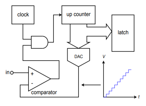
Figure \(\PageIndex{7}\): Staircase converter.
Successive approximation is a good general-purpose solution suitable for systems requiring resolutions in the 16-bit area. Instead of trying to convert the input signal at one instant like the flash converter, this technique creates the output bit by bit. Unlike the staircase converter, each individual level does not need to be tested. Instead, a binary search algorithm is used. You might think of it as making a series of guesses, each time getting a little closer to the result. Each guess results in a simple comparison. For an \(n\)-bit output, \(n\) comparisons need to be made.
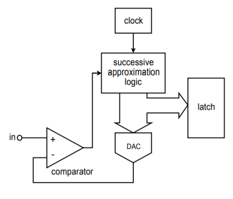
Figure \(\PageIndex{8}\): Successive-approximation converter.
A block diagram of a successive approximation converter is shown in Figure \(\PageIndex{8}\). Instead of a simple up counter, a circuit is used to implement the successive approximation algorithm. Here is how the circuit works. The first bit to be tested is the most significant bit. The DAC is fed a 1 with all of the remaining bits being set to 0 (i.e., \(100000 \dots )\). This word represents half of the maximum value capable by the system. The comparator output indicates whether \(V_{in}\) is greater or less than the resulting DAC output. If the comparator output is high, it means that the required digital output must be greater than the present word. If the comparator output is low, then the present digital word is too large, so the MSB is set to 0. At this point, the next most significant bit is tested by setting it to 1. The new word is fed to the DAC, and again, the comparator is used to determine whether or not the bit under test should remain at 1 or be reset. At this point the two most significant bits have been determined. The remaining bits are individually set to 1 and tested in a similar manner until the least significant bit is determined. In this way, a 16-bit system only requires 16 comparisons. With a 1 microsecond DAC, conversion takes only 16 microseconds. This translates to a sampling rate of 62.5 kHz; thus a maximum input frequency of 31.25 kHz is allowed. As you can see, this is far more efficient than the staircase technique.
For the highest resolutions combined with high sample rates, delta-sigma conversion techniques are popular. Basically, a low-resolution converter is run at a rate many times higher than the Nyquist frequency (perhaps 256 times higher). A special digital filter called a decimator converts the low-resolution high sample-rate data stream into a lower rate with higher resolution. This technique can achieve conversions in the 50 kHz range with 20-bit resolution. Design and analysis of delta-sigma modulators and digital filters is an advanced topic beyond the scope of this text. We will, however, look at a representative IC in the next section.
12.5.2: Analog-to-Digital Converter Integrated Circuits
In this section we will examine a few specific ADC ICs, along with selected applications. The ICs include the ADC0844, an 8-bit microprocessor-compatible unit; the ADC12181, a very fast 12-bit converter utilizing pipeling techniques; and the CS5396, a 24-bit converter designed primarily for audio applications.
ADC0844
A block diagram of the ADC0844 is shown in Figure \(\PageIndex{9}\). Along with the built-in clock and 8-bit successive approximation register (SAR), the IC also includes an input multiplexer, tri-state latches and read, write, and chip select logic pins. This means that the ADC0844 is easily interfaced to a microprocessor data bus and may be used as a memory-mapped I/O device. This IC is a moderate-speed device, showing a typical conversion speed of 40 microseconds. The timing diagram for the ADC0844 is shown in Figure \(\PageIndex{10}\). A conversion is initiated by bringing both the chip-select and write-logic lines low. The falling edge of write resets the converter and its rising edge starts the actual conversion. After the conversion period, which is set internally, the digital data may be transferred to the output latches with the readlogic line. Note that the pulse repetition rate of the write-logic line sets the sampling rate. Therefore, a small program running on the host microprocessor that reads and writes to the ADC may be used to control the sampling rate and store the data for later use.
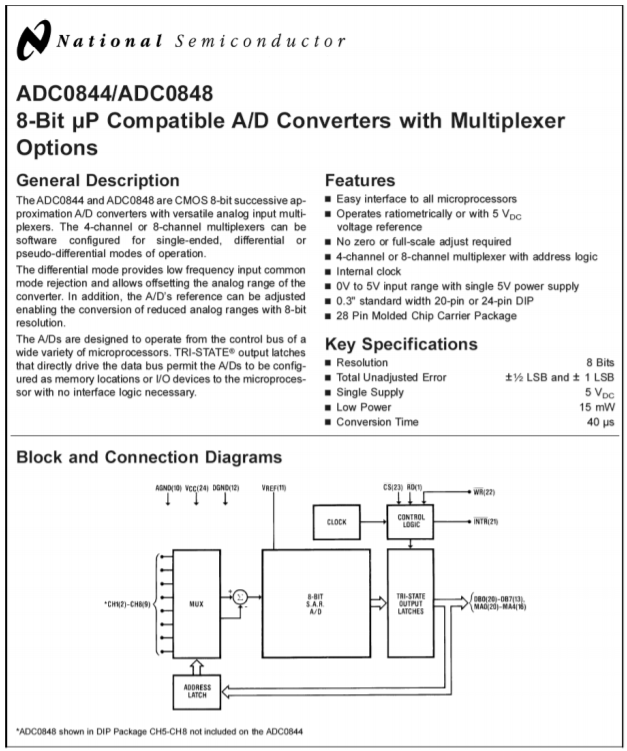
Figure \(\PageIndex{9}\): The ADC0844. Reprinted courtesy of Texas Instrutments
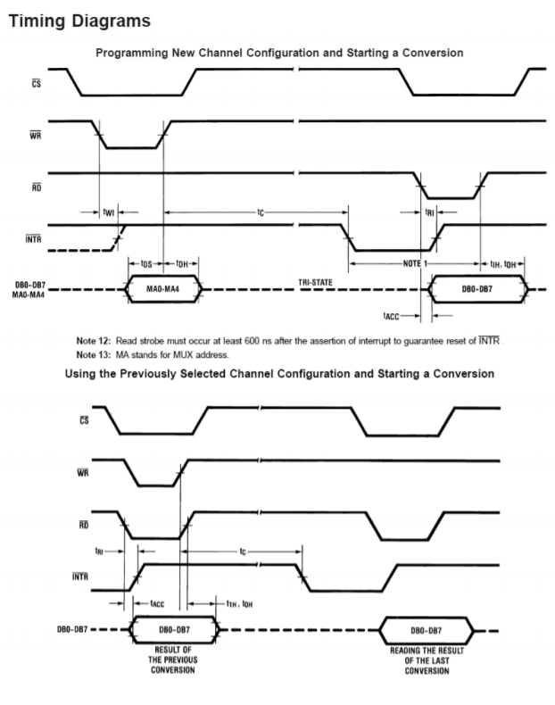
Figure \(\PageIndex{10}\): Timing diagram for the ADC0844. Reprinted courtesy of Texas Instrutments
LTC2282
The LTC2282 is a 12-bit, 105 mega-samples per second converter with an internal sample-and-hold. Its data sheet is shown in Figure \(\PageIndex{11}\). In order to achieve its combination of high sample rate with relatively high resolution, the LTC2282 relies on a technique known as pipelining. In this particular chip, the pipeline consists of six stages. Each stage produces a digital signal of just three bits and an error signal known as a residual. The residual is passed to the following stage where it is multiplied by a fixed gain, thus bringing it up to the former bit-weight. The newly resulting residue is passed to the next stage where the process is repeated. In essence, the signal propagates down the pipeline in a fashion conceptually similar to the successive approximation technique. Note that pipelining speeds the conversion process because once the residual is passed to the next stage, the prior stage(s) can begin work on the following sample(s).
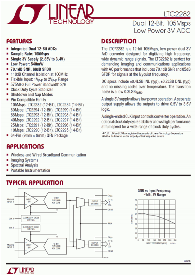
Figure \(\PageIndex{11a}\): LTC2282. Reprinted courtesy of Linear Technology
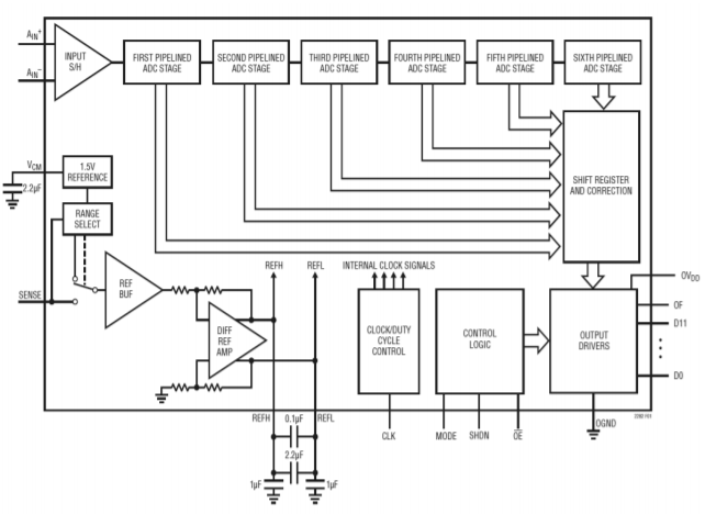
Figure \(\PageIndex{11b}\): LTC2282 block diagram. Reprinted courtesy of Linear Technology
The LTC2282 is used for applications requiring both high speed and high resolution. It also offers self-calibration, single +5 V power supply operation, and low power consumption.
CS5381
The CS5381 offers stereo 24-bit resolution with a maximum sampling rate of 192 kHz. This is ideal for a wide range of high-quality digital audio systems. The CS5381 data sheets are shown in Figure \(\PageIndex{12}\). This IC uses the delta-sigma conversion technique and achieves a dynamic range of 120 dB. The signal-to-noise plus distortion rating (THD+N) is typically 110 dB. The device over-samples the input at 6.144 MHz and has logic settings for 1X, 2X and 4X effective conversion rates at its output. For example, the standard pro-audio sampling rate is 48 kHz with double rate at 96 kHz and quad rate at 192 kHz.
As with any high-resolution converter, you must be particularly careful with the circuit layout or excessive noise may result. Attention must be paid to proper power supply bypassing. The CS5381, like many ICs in this category, requires separate analog and digital power supplies. Although this IC only requires 5 V, note that there are separate physical connections for analog and digital power. Standard logic supplies are often too noisy for use on such precision devices and will degrade overall audio performance when applied to the analog portion of the IC.
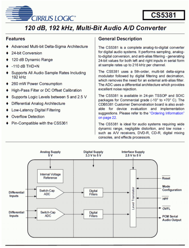
Figure \(\PageIndex{12a}\): CS5381. Reprinted courtesy of Cirrus Logic, Inc.
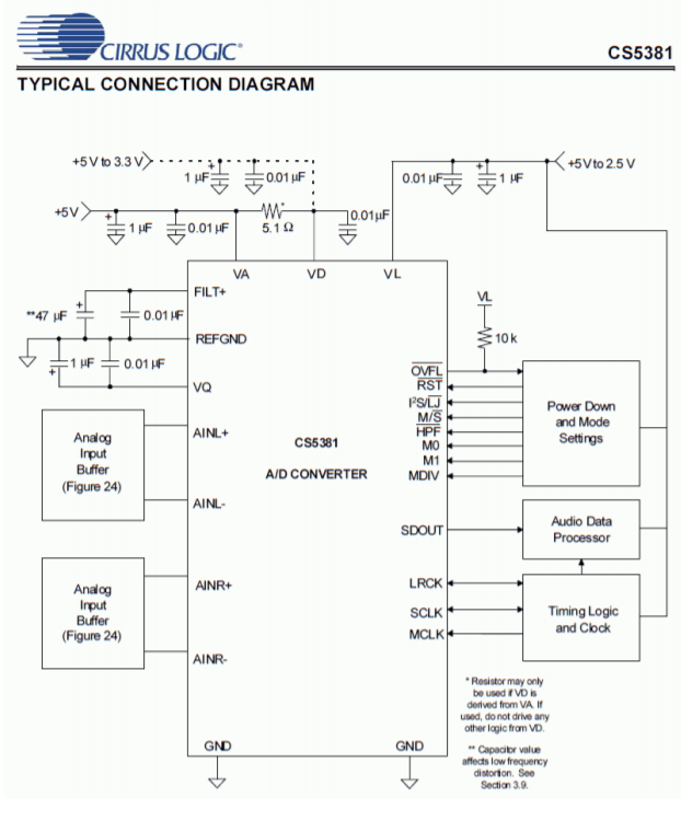
Figure \(\PageIndex{12b}\): CS5381 connection diagram. Reprinted courtesy of Cirrus Logic, Inc.
12.5.3: Applications of Analog-to-Digital Converter Integrated Circuits
Example \(\PageIndex{1}\)
Perhaps the most straightforward application of analog-to-digital conversion is the acquisition of a signal. Once in the digital domain, the signal may be processed in a variety of ways. An example of this is the Digital Sampling Oscilloscope (DSO). A simplified block diagram of a DSO is shown in Figure \(\PageIndex{13}\). Since the final output of the system is a simple graph, it generally does not make sense to resolve the input beyond 8 bits (256 steps), and often even fewer bits may be used. Typically, high sampling rates are more important than fine resolution in this application. Consequently, 12- and 16-bit converters are not found here. Instead, lower-resolution converters capable of sampling at hundreds of MHz are used.
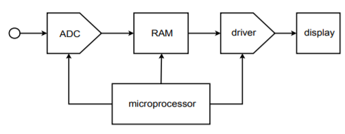
Figure \(\PageIndex{13}\): Basic digital sampling oscilloscope.
DSOs can usually be run in one of two modes: continuous, or single-shot. In single-shot mode, the ADC acquires the signal and stores it in memory. This data can then be routed to the display circuits continuously in order to create a trace on the display. The signal is captured and stored in computer memory, thus it can be replayed virtually forever without a loss of clarity. This is very useful for catching quick, non-repetitive transients. Once the signal is captured, it may be examined at leisure. For that matter, if some form of level-sensing logic is included, sampling can be initiated by specific transient events. This is known as baby-sitting. For example, you might suspect that a circuit you have designed occasionally emits an undesirable voltage spike. It is not practical for you to hook up the circuit and stare at the face of an oscilloscope, perhaps for hours, waiting for the system to misbehave. Instead, the DSO can be programmed to wait for the transient event before recording. In this way, you can leave the system, and when you return some time later, the spike will have been recorded and will be waiting your inspection.
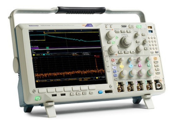
Figure \(\PageIndex{14}\): Commercial MDO. Copyright © Tektronix. Reprinted with permission. All rights reserved
An extension of this concept is pre-trigger recording. In this variation, the DSO is constantly recording and “throwing away” data. When the transient spike finally occurs, the DSO has a snapshot of the events leading up to the spike, as well as the spike itself. This can provide very useful information in some applications. In either case, since the data is in digital form, it may be off-loaded to a computer for further analysis. Indeed, many DSOs offer some interesting on-board analysis functions, including signal smoothing (noise reduction), trace cursors which allow for easy delta time/delta voltage computation, basic math functions, spectrum computation via FFT and more.
In continuous mode, a DSO appears to operate in much the same fashion as an ordinary analog oscilloscope. In this mode, the DSO samples the input signal and passes the data out to memory. From here the data is relayed to the display circuitry where a trace is produced. The trace is being constantly updated, so any change in the input will be quickly displayed.
The basic concept of the DSO has been expanded to the MSO and the MDO. The MSO, or Mixed Signal Oscilloscope, adds digital domain measurements while the MDO, or Mixed Domain Oscilloscope, extends the MSO into the frequency domain as well.
Example \(\PageIndex{2}\)
Another interesting application of the analog-to-digital converter is in the digital sampling music keyboard or drum computer (generally referred to as a sampler). The usage of a sampler is quite straightforward, actually. The idea is to mimic the sound of a given instrument (such as a trumpet or flute) from the keyboard. Before the advent of the sampler, this was done by properly setting the filters, amplifiers and oscillators of a keyboard synthesizer. Although the resulting sounds were reasonably close to the desired instrument, they usually weren't close enough to fool the average listener. The sampler bypasses the problems of synthesizers by directly recording an instrument with an analog-to-digital converter. For example, a trumpet player might sound an \(A\) into a microphone that is connected to the sampler. This note is digitized and stored in RAM. Now, when the keyboard player hits the \(A\) key, the data is retrieved from RAM and fed to a DAC where it is reconstructed. The result is the exact same note that the trumpet player originally produced. By recording several different pitches from many different instruments, the keyboard player literally has the power of an entire orchestra at his fingertips. Of course, there is no limit to the sounds that might be sampled, and the keyboardist could just as easily use the sampler to “play” a collection of dog barks, door slams, and bird calls. A sampling drum computer is similar to a sampling keyboard, but replaces the standard musical keyboard with a series of buttons that allow the musician to create a programmed sequence of notes. This sequence can be played back at any time, and at virtually any tempo. In this manner, an entire percussion section may be simulated using digital recordings of real drums. A block diagram of a typical musical sampling system is shown in Figure \(\PageIndex{15}\).
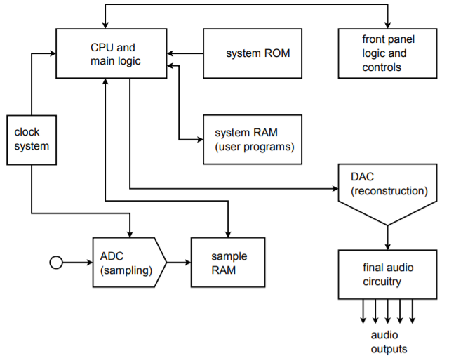
Figure \(\PageIndex{15}\): Block diagram of musical instrument sampling and playback device.
Further enhancements to the digital sampling musical instrument include direct connections to personal computers. In this way, the computer can be used to analyze and augment the sound samples in new ways. For example, the personal computer may be used to create a graphic display of the waveform, or compute and display the spectral components of the sound using a popular technique called the Fast Fourier Transform. An example is shown in Figure \(\PageIndex{16}\). Finally, the computer can be programmed to “play” the sampler. In this way, even non-keyboardists can take advantage of the inherent musical flexibility this system offers.
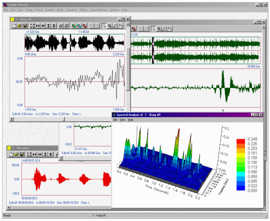
Figure \(\PageIndex{16}\): Commercial waveform display and editing software. Reprinted courtesy of dissidents