
12: Case Study on Nanotechnology
- Page ID
- 43056
Here we delve into a case study on nanotechnology which is an ancient technology as well as a cutting-edge modern technology. This contradiction is exactly why this is an interesting case study for learning what engineering (and science) is all about.
This section is meant to be accompanied with an inexpensive textbook. Fortunately wikibooks has such a textbook (free): The Opensource Handbook of Nanoscience and Nanotechnology
This book is an excellent if a bit incomplete introduction (for an engineer or scientist) to nanotechnology. Some of the topics however might be overly advanced for an introduction to engineering class, so in this section nanotechnology will be reviewed with an assumption that the student will use the textbook above (or another one of their choice) to supplement. This section is not meant to take more than a week in an actually instructive setting.
What is naontechnology?
To begin with let us do another class discussion that asks the question: What is nanotechnology? Discuss before looking at some answers.
- ¬ What is nanotechnology?
- Technology in the nanometer range of measurement, ok, what does that mean????
- ¬ What does technology in the nanometer range mean?
- We can generally agree that technology is the products or technique of scientists and engineers. For nanotechnology it means that at least one of the dimensions is in-between 1 nm to 100 nm (with round off). So a buckyball (C60) with a diameter of 0.7 nm is nanotechnology (because it rounds off to 1 nm). A carbon nanotube (CNT) with a diameter less than 100 nm but a length over 100 meters long is nanotechnology. But what does nanometer really mean? What size is "nanometer"?
- ¬ So what is nanometer really mean?
- Let's talk about scales then. The best way to do that is to just look at a YouTube of the Powers of Ten (the 1977 original version; note that 1 Ångstrom is 10 nanometers)1.
- ¬ Given the scales you have seen what is nanotechnology now?
- Nanotechnology is technology at the molecular level, so it could be called molecular technology. This differs from say microtechnology (MEMS - microelectromechanical systems) which is closer to cellular size. MEMS are very small machines that still act in a classical way which is different from systems in the nanometer range. Molecular technology is about the smallest we can go with technology as after this we would go into the atomic realm (just a few atoms at best) which would not be enough to form anything that is regarded as technology, though it certainly is still science. So we would have to say no to the idea of picotechnology. Nanotechnology is small enough to have characteristics that are not the same as we would expect at micro and above sizes.
- ¬ Nanotechnology, while something humankind manipulates, is natural as well. Can you think of a food technology were we use nanotechnology?
- Bread making! We use yeast to breakdown starch to produce sugar which is then digested by the yeast which produces the byproducts of carbon dioxide and ethanol. This is then baked to make a nice light tasty bread. The first use of this is believed to be by accident by Ancient Egyptians (though it might have been earlier) when they would leave "flatbread" out too long and natural yeast would "contaminate it." When baked this contaminated flatbread produce something that was not the old-fashion flatbread but something new, different, and tasty. Later humankind intentionally grew yeast for the purpose of making bread (and a slightly different one for beer). Hence we used nature to do some of our first nanotechnology.
- ¬ What about a product developed in ancient Egypt (or maybe earlier) that is nanotechnology?
- That's right, stain glassed windows! Nanoparticles of metal actual show up as different colors and that was utilized by the stain glass industry of which ancient Egypt and Rome had many products. Depending on how you grind up metals (like gold, copper, silver, etc.) you can observer different colors such as red (gold), orange, green, and yellow (silver). The nanoparticle size2 of the metal will determine the color you observe.
- ¬ However even before humankind started using nature to assist us in nanotechnology, an amazing piece of nanotechnology already existed billions of years before humankind. This nanotechnology is a technology that we might someday be able to employ to do work for us one day. What is this technology?
- Ribonucleic acid (RNA) and Deoxyribonucleic acid (DNA)...the code of life. RNA (mRNA in particular) is already employed for vaccines (first application was COVID-19 vaccine). DNA offers a kind of computer program to build anything from a fruit fly to a human being (with very little variability as a fruit fly's DNA is about 60% identical to human DNA).
- ¬ Can you think of any other natural nanotechnology?
- Oxygen generation is the process of a RuBisCo (an enzyme - nanotechnology) reduction that has as a discarded product oxygen which turns out to be pretty important to life especially with animals that have skeletons.
Carbon allotropes
Because "buckyballs" are the start of the modern revival of nanotechnology (at least from a media point of view) let us go over some of carbon allotropes that are making headlines.
Buckyballs
While nanotechnology is an old technology, a new modern revival of the technology came about with discovery of C60 or the Buckminsterfullerene (buckyball) named after Buckminster Fuller because of his penchant for building geodesic domes. Why geodesic domes? Because these domes are based off the Platonic solids3 and C60 is a truncated icosahedron (one of the Platonic solids).
C60 were produced in 1985 during an experiment to help understand certain carbon molecules that might have been generated in space. Why do such an experiment? Because most stars have debris surrounding them with carbon in it and some have very long chains that are of interest to astronomers. Hence the experiment. The actual generation of C60 was not intended but serendipity. From an engineering and science point of view, the analysis after the experiment was the real research because C60 was identified through analysis after the experiment that did not aim to produce them or even know of their existence.
The buckyball is now considered a part of the fullerene family. An outline of facts about buckyballs:
- Truncated Icosahedron (like a Telstar football or "a soccer ball circa 1970s")
- 0.7 nm in diameter with a spacing of about 1 nm between adjacent buckyballs
- Inert
- Can be made into a superconductor
- Offshoot studies led to the discovery of the carbon nanotube (next topic)
- Has been detected in burning candles (a modern addition to Faraday's The Chemical History of a Candle, yes?)
- Buckyballs have been found in space officially by the satellite Spitzer
- Stacked buckyballs
- A huge amount, not miniscule
- The most massive particle to show wave-particle duality (Nature 1999)
There are many articles about buckyballs and interesting uses of buckyballs (though some are totally false, so be careful! See Understanding). In this brief review though we will move onto the carbon nanotube as there have been actual products developed from this fullerene. That's not to say that buckyballs will never have products produced from them, there time just hasn't come yet.
Carbon Nanotubes
Carbon nanotubes were first observed in 1991 and produced in 1992. Because of this discovery interest in buckyball technology shifted to these nanotubes. Carbon nanotubes are like an individual layer of graphite (which is now called graphene) that is wrapped around to meet end to end. An outline of facts about carbon nanotubes:
- Extremely strong
- Known as buckytubes at one time
- Found in Damascus sabers, an extremely strong and flexible saber in the 13th century and beyond (Nature 444, 286, 2006)
- Science in making the sabers but serendipity that CNTs were involved (just like bread making, etc.)
- Modern techniques make better sabers, but at the time they were the best (and their legend lives on)
- Varying diameters from 1 nm to 100 nm and can in theory be as long as you desire, but in practice not so long (yet)
- Good conductor of electricity
- Or can be a semiconductor
- Called (carbon) nanowires when discussing electrical properties (note: this is not the only type of nanowire)
- Single-walled (SWCNT or SWNT) and multi-walled (MWCNT or MWNT)
- Forest of MWCNTs can produce the blackest substance known this is very important for astronomical purposes (telescopes)
- Buckypaper offers many possible applications, but still is in its infancy
- GSFC/NASA continues their groundbreaking work on carbon nanotube technology
- CNT has been tested for such diverse ideas such as water filtration, supercapacitors, heat shields, etc.
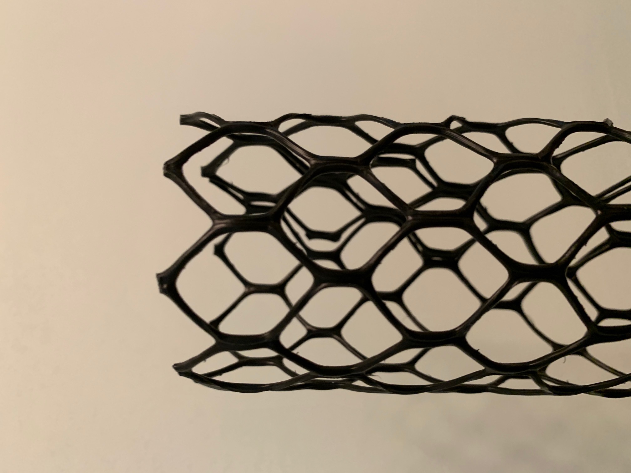
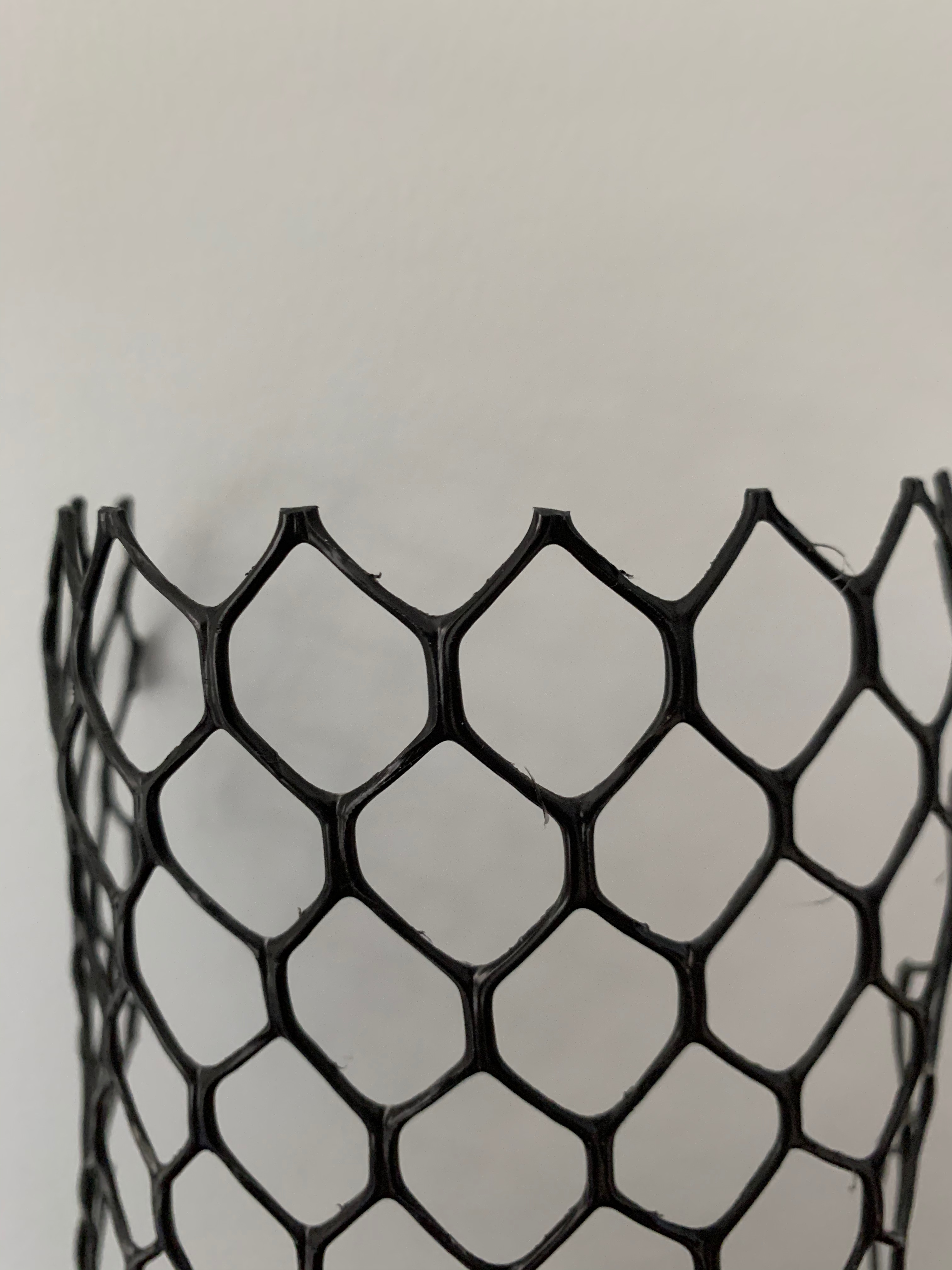
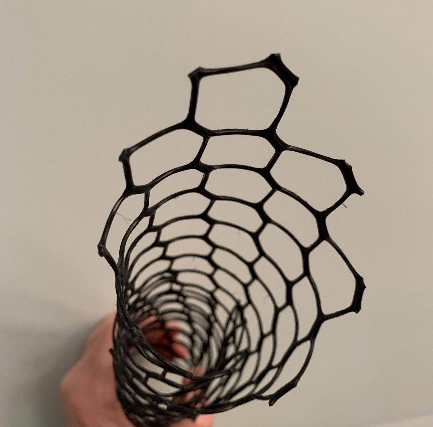
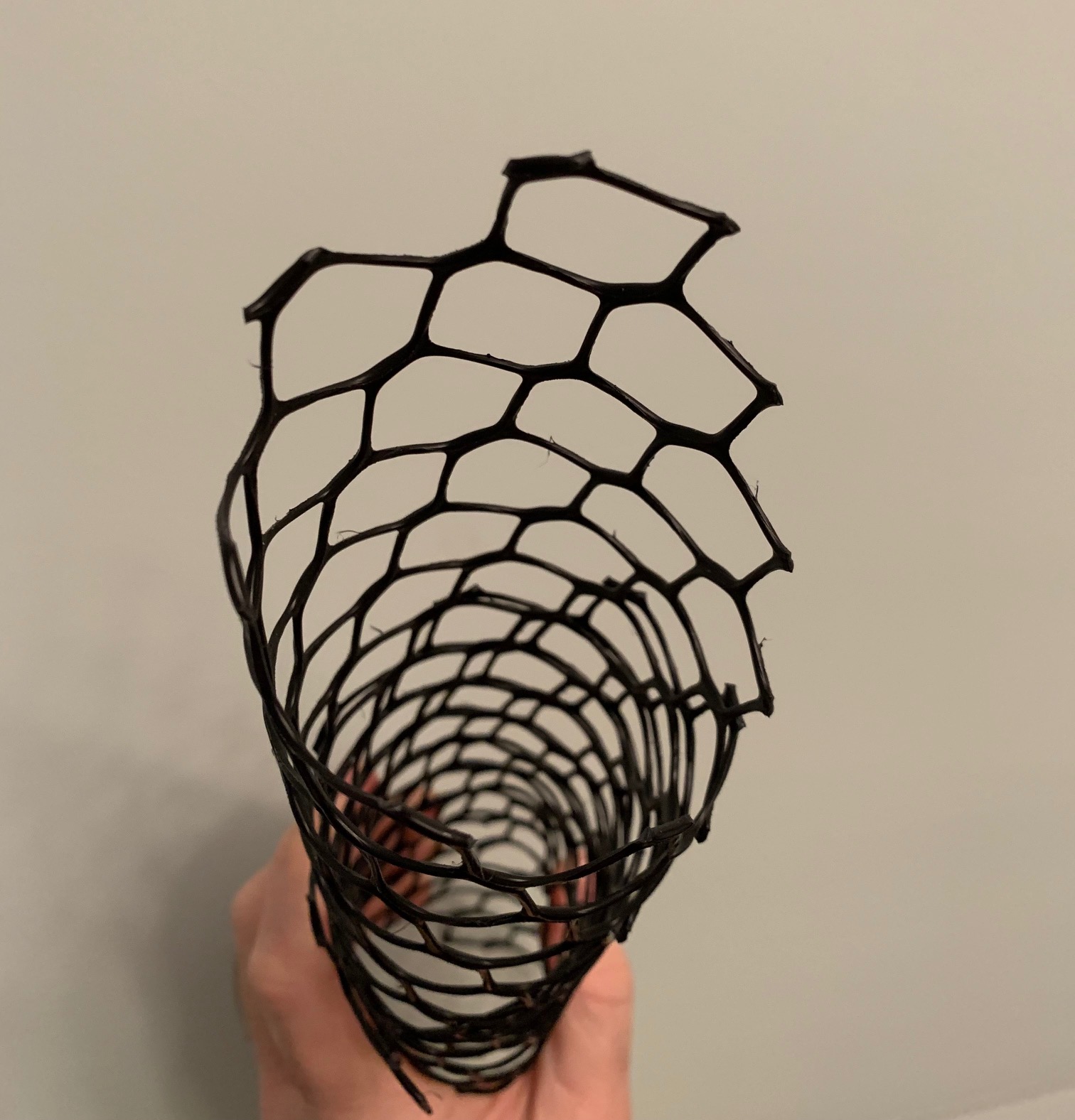
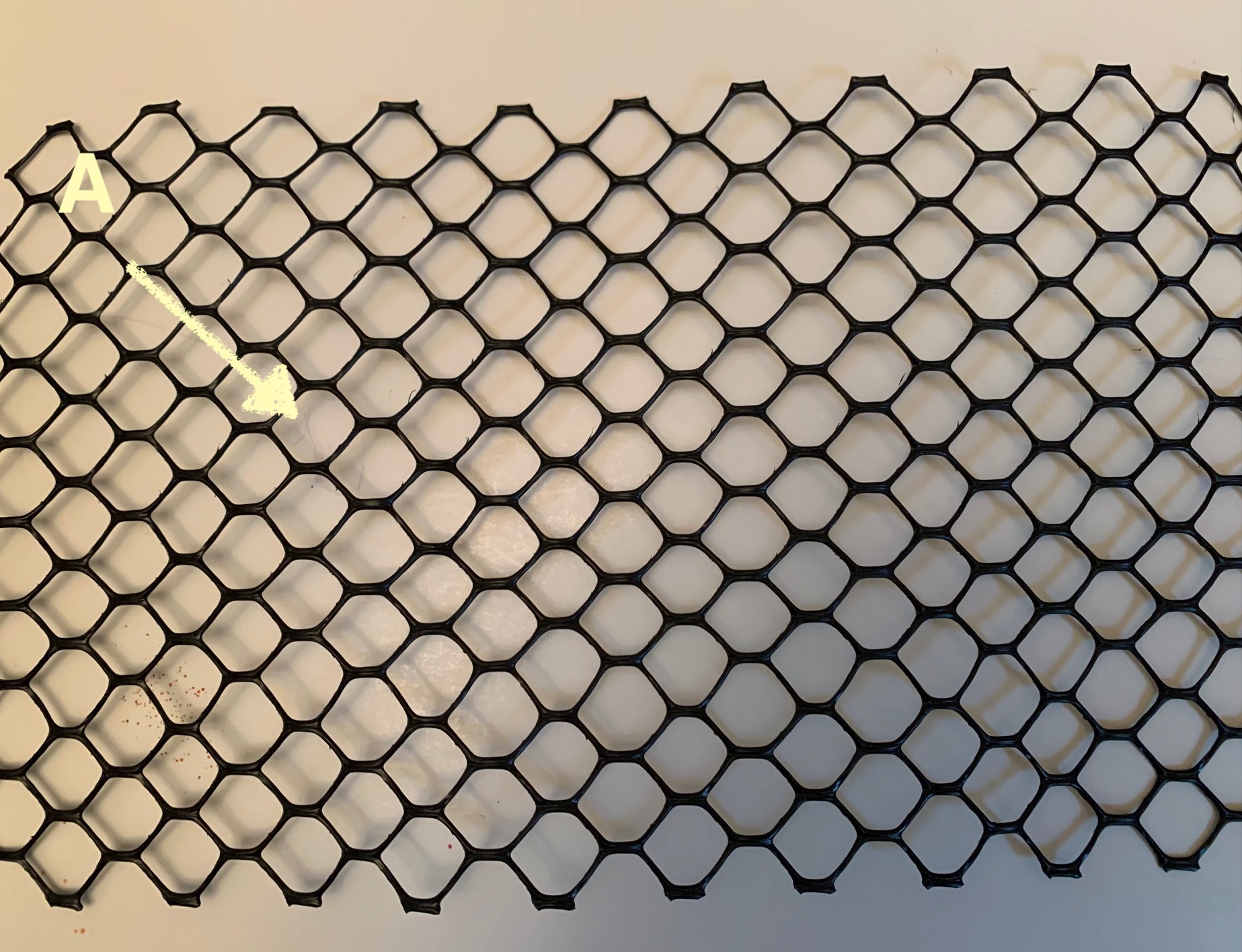
A great way to look at nanotubes is to get a piece of chicken wire (plastic preferably) and cut out a rectangle (at this point you have graphene) and wrap it around (nanotube). You can do this at home which is way better then a flat screen simulation and definitely inexpensive.
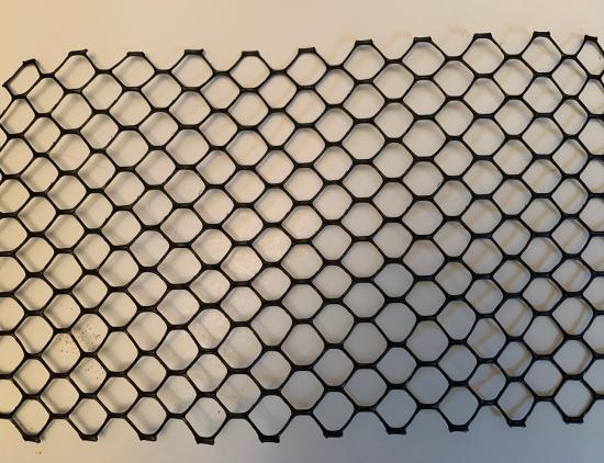 |
| Chicken wire to represent one layer of graphite which is called graphene. Graphene will be discussed later in the chapter. |
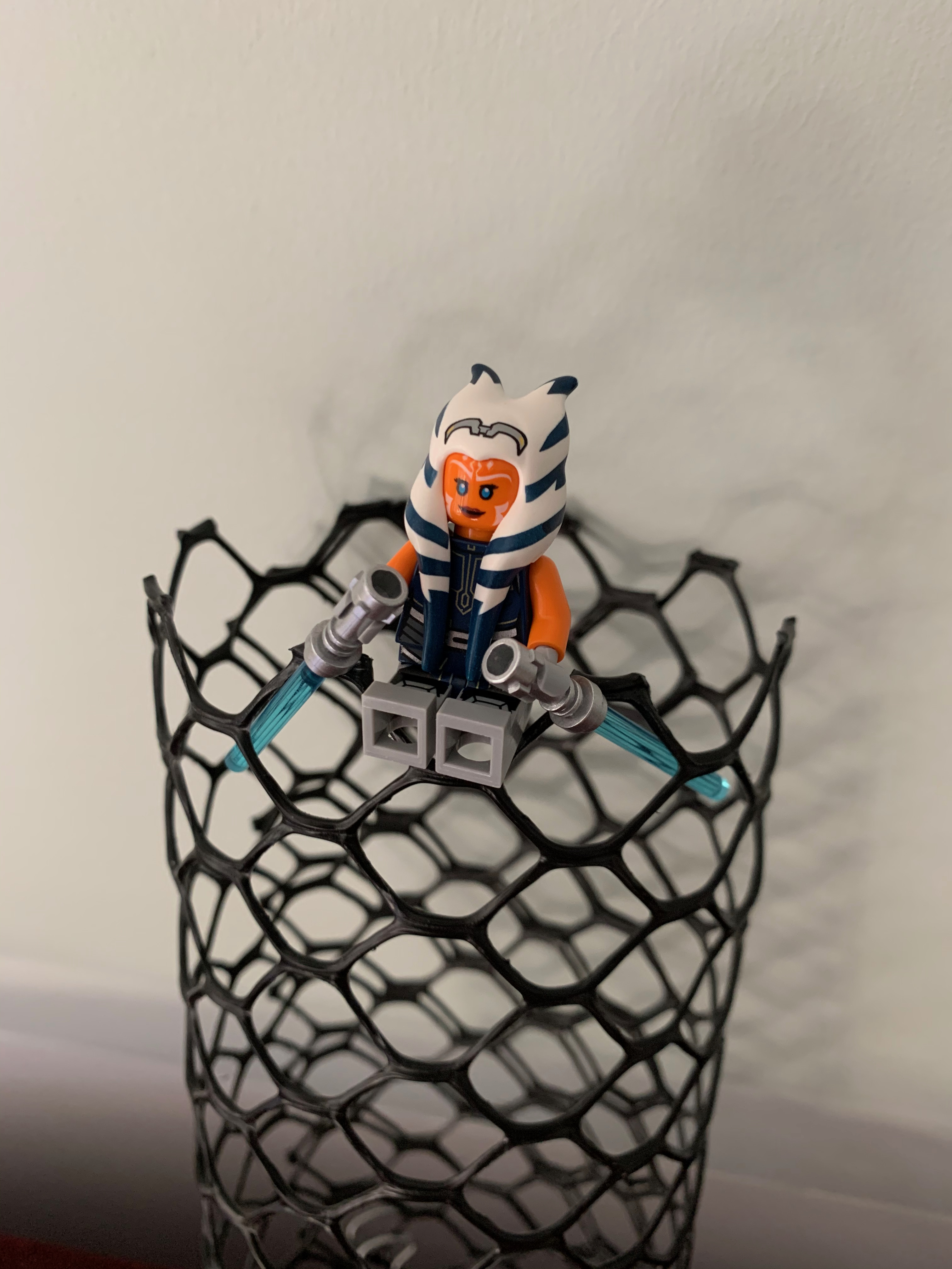
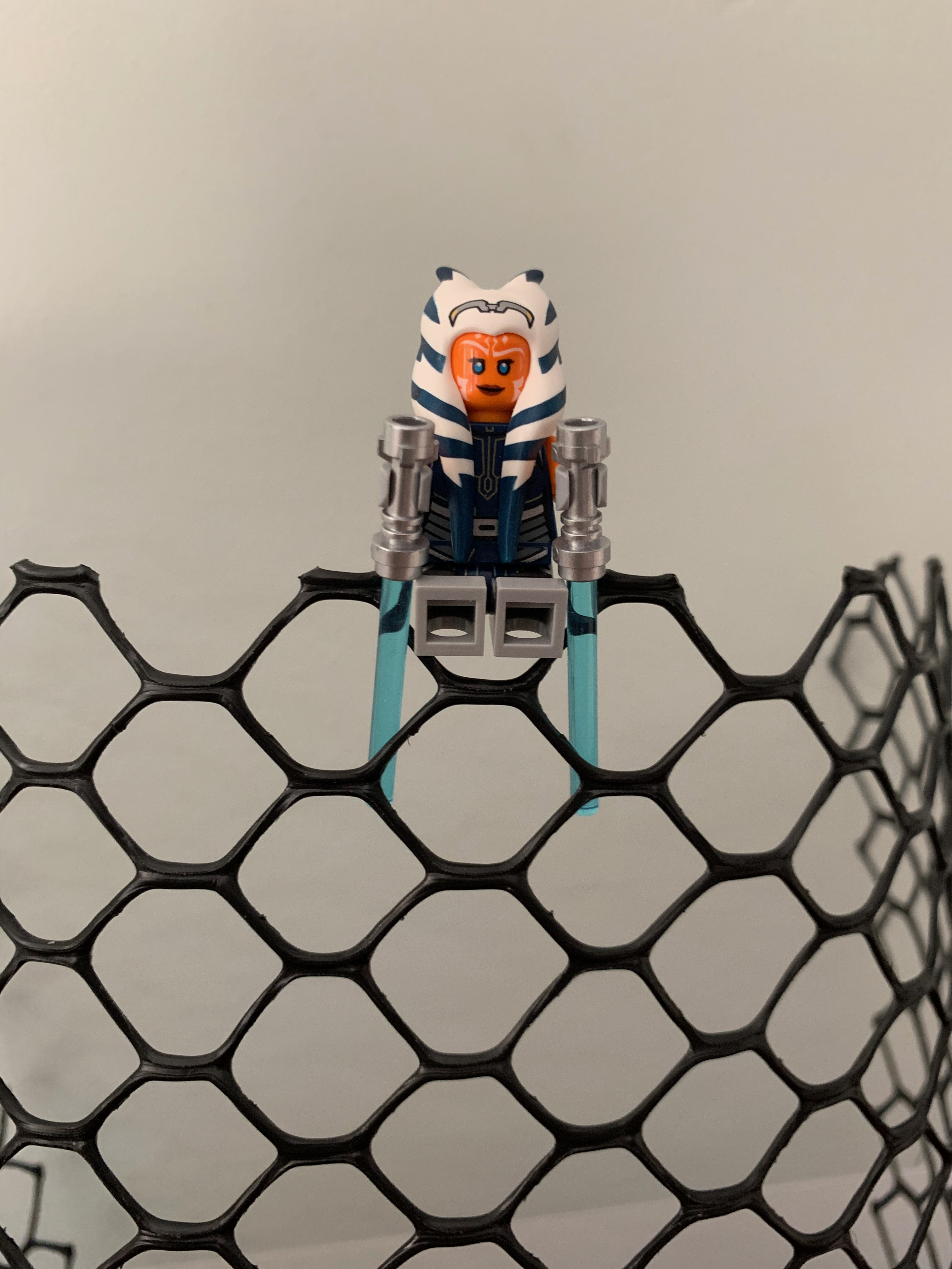
Different wraps of graphene can produce different properties for carbon nanotubes. That is, depending on how you wrap the nanotube you can have metallic nanotubes or semiconductor nanotubes (or at this point you might want to call it a nanowire). Note that the ends of the wrap which normally don't have a cap in our representations represents the end of the nanotube itself.
 |
 |
 |
 |
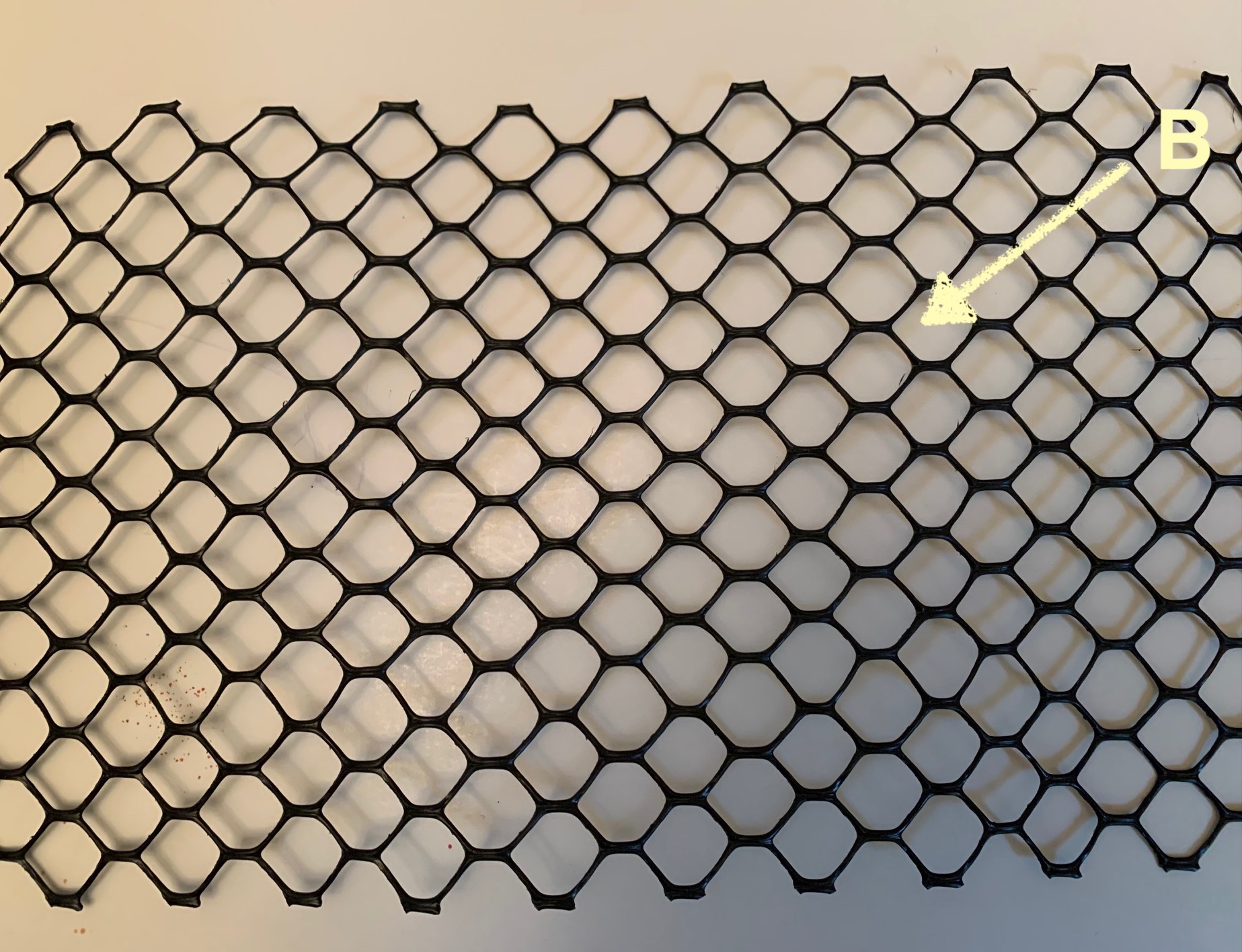
| Armchair wrap of the "graphene" from the image above. This warp will give you a very good conductor. | Armchair wrap. Here Ahsoka is demonstrating why it is called an armchair. The wrap is not complete here because it obscured the visual aspect of the armchair. | Zig-zag wrap. This wrap produces semiconductor nanowires. | Zig-zag wrap. The warp is not complete so as not to obscure the visual aspect of the zig-zags. |
There are two other possible wraps for the carbon nanotube and that is the chiral wraps. Chiral CNTs are stereoisomers and are mostly semiconductors.
 |
 |
 |
 |
| Chiral wrap - delta isomer. This in essences is a twisted cylinder. Chiral wraps can produce either conductor or semiconductor nanowires. | Using the "graphene" sheet if we wrap the sheet starting at B in the direction of the arrow (right; clockwise) we will produce a chiral wrap at left. | Chiral wrap - lambda isomer. Chiral wraps can produce conductor or semiconductor nanowires. | Using the "graphene" sheet if we wrap the sheet starting at A in the direction of the arrow (left; counter-clockwise) we will produce the chiral wrap at right. |
For carbon nanotubes we can define a coordinate system that has unit vectors that help us describe the armchair, zig-zag, and chiral nanotubes.
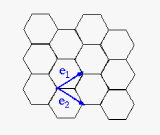
Using the unit vectors (\(\vec{e_1}\) and \(\vec{e_2}\)) defined in the figure above we can write an equation that describes the various nanotubes as \(m \vec{e_1} + n \vec{e_2}\) where m and n are integers and \(m+n \ge 2\). Given this equation if m or n equal zero then we have a zig-zag CNT (semiconductor), if m=n we have an armchair CNT (metallic), and otherwise it is chiral CNT. In general chiral CNTs are semiconductors but if \(\lvert (m-n)\rvert \) is a multiple of 3 then it is metallic4.
Fullerene research is just at its infancy and there will be more to discover which will include its share of disappointments, but that is science.
Graphene
So what about that sheet of graphite we discussed above? A single sheet of graphite is called graphene. Through studies of the laminar nature of graphite oxide starting as early as the 1860s where chemist Benjamin Brodie produced thin layers of the crystal which he studied and was able to get atomic weight of graphite. Studies on this structure continued with every thinner layers which had high strength and noteworthy optical properties. In 1947, physicist's P. R. Wallace produced a theoretical framework for graphene in order to understand the electronic properties of graphite. Work continued on thin layers of graphite both experimentally and theoretically with some work possibly being on graphene (there would be no way to distinguish between one and a few layers of graphite). In 1961 chemist Hanns-Peter Boehm reported on very thin layers of graphite flacks and called a single layer of graphite, "graphene." The term would be revived in the late 1990s when disscussing carbon nanotubes. Finally in 2004, physicists' Andre Geim and Konstantin Novoselov isolated and characterized free-standing graphene. And this is when things got interesting...
In the following outline we will list some properties of graphene that can possibly lead to exciting new products or are just very interesting scientifically:
- Graphene properties
- Single atom thickness (carbon)
- Graphene is a zero-gap semiconductor
- Normally a semiconductor has a greater than zero band gap and it is metals you would expect to have no band gap
- Graphene for a single atom layer has an unusually high opacity from visible to near infrared (and maybe mid infrared)
- That is the graphene actual absorbs light (over 2%)
- This feature mean you can actual "see" graphene in certain conditions
- Graphene's strong interaction with photons maybe useable for nanophotonics
- Graphene is theoretically an excellent material for spintronics due to carbon coupling and long spin lifetimes (theory)
- Graphene is mechanically very strong
- Lightest strongest material with large tensile strength
- Small spring constant (flexible)
- Very robust
- Graphene is brittle (like ceramics and not like metals)
- But it has a impressive ability to distribute the force of an impact
- This allows it to bend like metals
- Graphene has high surface area to mass ratio (almost goes without saying) which could make it good for supercapacitors (instead of the currently favored idea of activated carbon)
- It is possible to sculpture graphene into a honeycomb shape referred to as 3D graphene
- Can by used for energy storage, filtration, and other applications
That was just a few of the interesting properties of graphene. But this is not the last word on nanotechology as up and coming new technology includes the hexogonal Boron Nitrite (h-BN) that has just as many interesting properties as graphene. And we can go even further with combining fullerenes, graphene, and h-BN. Already combining graphene with CNTs has produced interesting research avenues as well as graphene with bismuth nanowires and graphene with h-BN (hexagonal Boron Nitrite).
So let us move on to discussing nanotechnology in more general way to give just a brief overview.
Nanotechnology by discipline
Nanotechnology spans multiple engineering disciplines which we will list briefly below. For electrical engineering the processes of making integrated circuits (ICs) has been in the nanotechnology range for decades, but new techniques are possible with nanotechnology elements.
- Bioengineering
- Bionanosensors
- Utilizing natures nanotechnology (like mRNA for vaccines, etc.)
- Chemical Engineering/Food Engineering
- Nanofoods (nano-manipulation of food to improve taste, texture, etc.)
- Nanopackaging (using nanomaterials to improve packaging)
- Environmental Engineering
- Nanomembranes (for filtering)
- Nanocatalysts (for water remediation)
- Materials Science Engineering (can include Mechanical/Civil/Chemical/Aerospace/etc.)
- Nanocoating (including CNT coating)
- Nanosurface protection (including uses of CNT mechanical properties)
- Quantum dots
- Electrical Engineering
- Lithography (been at nano-level for a long time)
- DNA nanoarray
- Nanowires or nanosemiconductors
- Nano-optics
The outline above is just a taste of nanotechology and how it effects a number of engineering disciplines.
There are three different areas of research in nanotechnology which usually are the domain of different disciplines.
- "Wet" nanotechnology
- Liquid environment
- Usually biological
- Membranes
- Filters (CNT) and example of cross-over technology
- Dry nanotechnology
- Silicon and other inorganic materials
- Metals, semiconductors
- Too reactive so they can't operate in wet conditions
- Computational nanotechnology
- Modeling and simulation of complete nanostructures
- This should be in addition to actual experimentation and prototyping
- Be careful of papers that say they have discovered something but it is actual a simulation (you see this a lot)
- While this is important and could produce some excellent product or insight, it still has to be verified experimentally
- So don't get excited until the process is complete
- This is required to fully understand nanotechnology
- Modeling and simulation of complete nanostructures
What is so exciting about Nanotechnology?
The physical rules of the "macro" world are relevant all they way down to the microscopic level, but things change when you pass into the nano realm. Surface effects, chemical effects, optical effects, and physical effects are different in the nanoscale when compared to the macro or micro scale.
- This creates new and interesting products like
- Stain resistant clothes
- Sweat absorbing clothes
- Antimicrobial socks
- This creates new avenues of research
- New exciting discoveries await
- However, disappointments await as well
- This is the nature of research
- Of course, going back to the history lecture, funding is essential
- Is some money going to be wasted? Yes that is the nature of searching for things. "Failure" is an integral part of engineering and science. We want success but we want to progress as well and that means some failures
- Can we predict where our money should go? Yes and no. Simulations can give us clues, but it is not a perfect solution
- Should we only do research that is proven out by a simulation? No, but we should not ignore the contribution of simulation
Understanding the different effects at the nanolevel requires an understanding of physics. For engineers and scientists this is why physics is essential. Some ideas require a graduate level physics background, but even with a calculus-based physics understanding the ideas behind nanotechnology become clearer. Simulations are going to require graduate school level education.
- Some concepts that are important
- Scaling laws
- Quantum mechanics
- Transport phenomena
- Hartree-Fock (computational physics - approximation method for wave functions)
- Surface theories
- Hydrophobic and hydrophilic
- Diffusion, transport in all dimensions
Practical ways to do Nanotechnology
How do you go about making something in nanotechnology? There are two methods
- Top-down
- Building nanotechnology using larger elements
- Primary method in manufacturing at present
- No atomic-level control
- Nanophotolithography
- State of photolithography for a couple of decade
- Uses deep UV laser light
- Laser is a larger element producing smaller nano-element
- Bottom-up
- Build from molecular components
- Self-assembly
- Static self-assembly utilizes nature to reach minimum free energy
- Dynamic self-assembly requires energy to force a solution
- Molecular recognition
- That is components assemble themselves based off of a code
- Need some form of coding
- What in nature might be used as a model for this?
- What are some problematic issues with using this method?
The answer to our coding is DNA which we discussed at the start of this chapter.
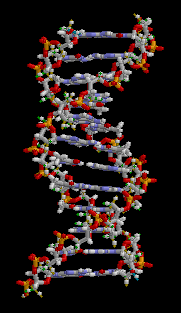 |
|
DNA animation, the code of life, and maybe the code to build nanotechnology in the future. https://commons.wikimedia.org/wiki/F..._animation.gif, brian0918, Public domain, via Wikimedia Commons |
DNA is a coding device that is used in nature, but some have proven it can be used by humans. DNA is nanometer in size. Let us view a TED Talk by Paul Rothemund explaining his creation of DNA faces.
Note that the method described here is not the only method people are researching. You can go to the Rothemund Lab web page (under research) to get links to other researchers in the field.
Nanotechnology Examples
Because nanotechnology is so vast and covers so many disciplines we have picked only a few examples as a way of introduction. There are many many many more applications and examples in the literature. We encourage you to read as many as you can. And maybe one of your essays can be on nanotechnology in your field!
Bismuth Nanowires
Bismuth in has been used in one form or another for thermocouples and thermopiles for more than a century. Bismuth is a semimetal even in nanowire form until about 50 nm when it transitions to a semiconductor form. Most research is done, however, with Bismuth nanowires in the semimetal form as it is difficult to produce good nanowires below 50 nm (though advances continue). Nanowires offer different properties that can aid in the thermocouple/thermopile are of research such as optical properties and reduction of thermal conductivity (bulk semimetal general dissipate energy to quickly due to higher thermal conductivity.
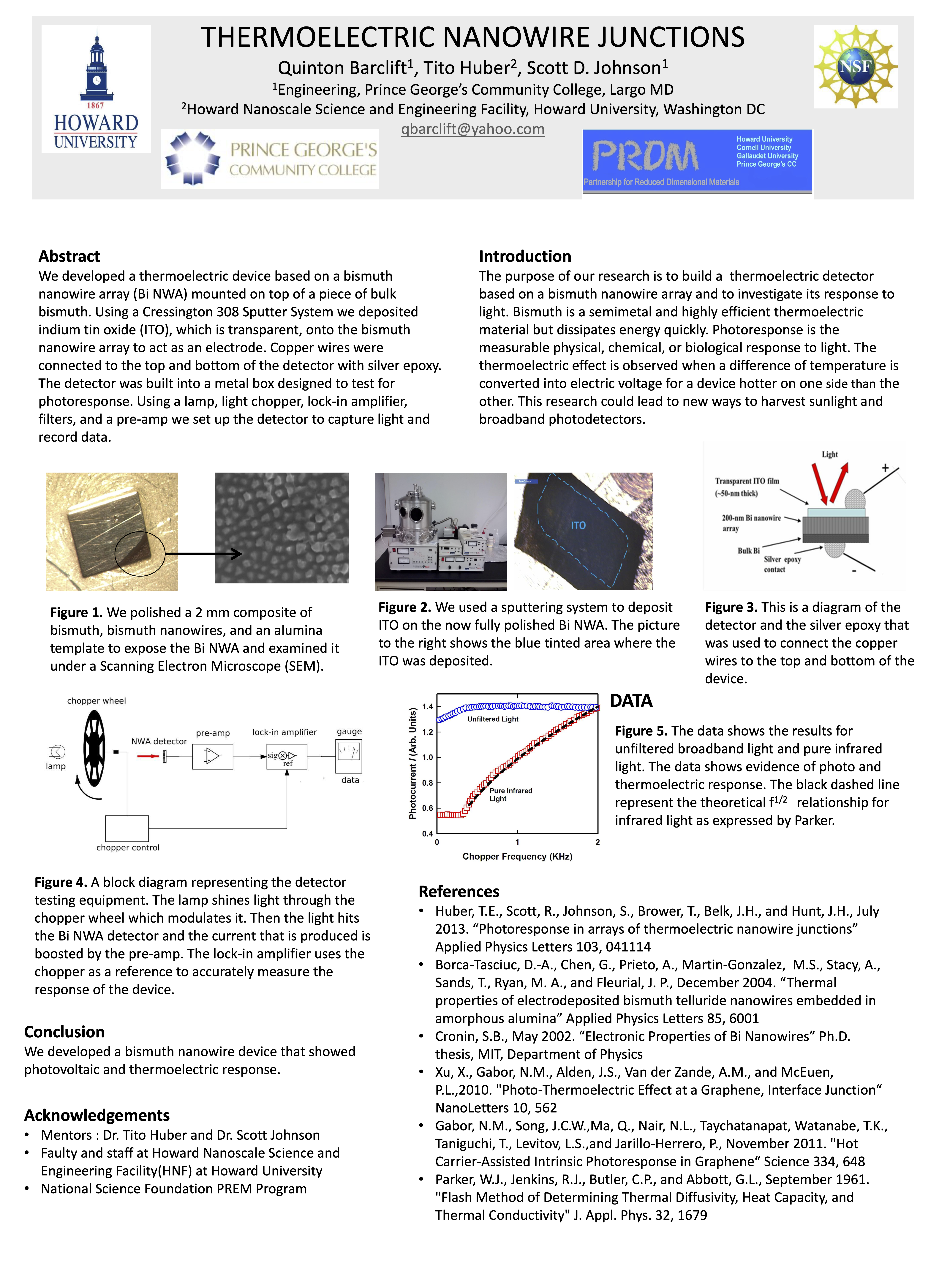 |
| This presentation discusses one application of nanotechnology. As a bonus this presentation also included an example of a detector testing system that is a classic chopping method for getting small signal response which is important in engineering beyond nanotechnology. |
Nanotechnology and the environment
- Water purification
- Humans need clean consumable water for survival
- Environmental contaminates are a serious problem that reduces the amount of consumable water to unacceptable levels
- Nanotechnology to the rescue?
- Ceramic nanomembranes
- Ultrafiltration
- Added reactive component (iron oxide ceramic membranes) add an extra-level of removal of contaminates
- Aluminum oxide ceramic membranes are another membrane being investigated
- Iron remediation
- Iron oxidization causes certain organic molecules (including toxic ones) to break down
- As the scale of the iron particles are reduced the iron becomes more reactive (greater overall surface area)
- Therefore nanoscale iron can improve remediation
- Smaller size allows the iron to go further into the soil (percolation)
- Ceramic nanomembranes
Nanotechnology materials
- Nanocrystalline metals
- All metals are crystalline with the grain size (not particle size but a boundary feature in metals...take Materials for more info)
- The grain size is an important characterization of metal (regardless if we are taking nanotechnology or not) that defines among other things the yield strength
- The Hall-Petch equation defines the yield strength with regards to the grain size
- \(\sigma_y = \sigma_0 + \frac{k}{\sqrt{d}}\) where \(\sigma_y\) is the yield strength, \(\sigma_0\) and k are constants that depend on the particular metal, and d is the average grain size diameter
- The equation implies that smaller grain sizes give better yield strength
- Valid for microcrystalline structures and mostly valid for nanocrystalline structures (above 30 nm)
- Possible negative Hall-Petch effect below 30 nm
- Questions remain; studies needed
- Issues are worsening corrosion and creep as the grain size gets smaller
- Future shows promise however
- Polymers
- DNA
- RNA
- Ceramics
- Ceramic nanoparticles
- Possible bone repair (see next example)
- All metals are crystalline with the grain size (not particle size but a boundary feature in metals...take Materials for more info)
Nanotechnology and bones
A large portion of our bones are nanosize hydroxyapatite which could be repairable using bioactive and resorbable ceramics. The mechanism of this repair would be osteoinduction. This is a very promising research avenue.
Spintronics (or magnetoelectronics)
The idea behind spintronics is to develop electronics that uses the spin of the electron rather than the "movement" of the electrons. The promise of this technology is to make transistors smaller and faster.
- So why is this nanotechnology? An electron certainly is not in the nanometer range? Is it?
- Technically spintronics is not nanotechnology, however, nanotechnology offers the best approach for its practical use
- How?
- By creating ferromagnetic semiconductors that require layers that are only a few nanometers (\(\leftarrow\) there you go)
Nanotechnology Machines
Can there be nanotechnology machines? No, not really, nanomachines are not very practical. But nanoparts for use by microelectromechanical systems (MEMS) is possible. For nanoelectromechanical systems (NEMS) we will outline some possible parts without getting into the details of how to control the motion (some sort of voltage will need to be applied).
- Nanomotor
- Use multi-walled nanotubes
- One tube rotates inside the other
- Kinds of emulates rotational bearings
- Molecular actuator
- The nanomotor would be controlled by the use of a nanocrystal ram (sort of like a piston)
- Control by voltage in some fashion
- Nanoelectromechanical relaxation oscillator (RC oscillator; multivibrator)
- In general electronics this can be used as a clock or for blinking lights on a car
- This works using liquid metal droplets that exchange mass
- Utilizes surface tension (which in would be very strong at this scale)
- Nano-Pressure sensor using graphene
- Graphene has relatively small spring constant and therefore is relatively flexible
- Graphene is very robust as well
Tools used in nanotechnology
A microscope is an optical device that uses light to magnify the object it is viewing, because visible light has a wavelength between 400 nm to 800 nm. Typically a "microscope" can at best see an object about twice the wavelength of light that is used. This means a normal optical microscope could at best see about 1 \(\mu m\) which is in its name...a microscope. This would be cellular level. It is possible to infer some nanotechnology from a powerful microscope, but it would be better to use something else. Also there are UV microscopes, but still it would be better to use something else. So in this section we will go over the tools for nanotechnology.
- Electron microscopes (EM)
- Scanning electron microscope (SEM)
- Focused beam of electrons
- Electrons' wavelength is much smaller than 1 nm (so this will work for nanotechnology)
- 5 to 10 nm resolution; some special SEMs can get down to just less than 1 nm
- Surface scanner
- Transmission electron microscope (TEM)
- Electrons penetrate the sample (typically less the 1 \(\mu m\))
- Magnets used to manipulate the electrons into the sample
- 0.2 nm resolution (but field of view is severely reduced in exchange for this better resolution)
- Analytic electron microscope (AEM)
- SEM, TEM with equipment like spectrometers
- 0.1 nm resolution
- While there are versions that can be used in a liquid environment, these Liquid-phase EMs have limited uses
- Need to prepare certain samples by sputtering metal (like gold) on them
- Sample is placed in a vacuum of at least 10-4 torr
- New innovations allow for "desktop" Scanning electron microsopes
- Scanning electron microscope (SEM)
- Scanning Probe Microscopes (SPM)
- Scanning tunneling microscope (STM)
- Used electrical properties from tip to sample
- 0.1 nm resolution
- 0.01 nm depth resolution
- Atomic Force Microscope (AFM)
- Uses force properties (this is how it distinguishes from STM) using a cantilever
- Three modes
- Non-contact mode
- Detects the Van der Waals forces by oscillating very close to the surface
- Difficult mode to work because of its being close to the surface which induces troublesome forces
- Contact mode
- Most common mode
- Tapping mode
- For soft surfaces
- Non-contact mode
- Different probes5 that detect different things can be attached to most AFMs
- There are many different type of probes (maybe 100 or so)
- List of a few interesting probes (to highlight what can be done)
- Nanoscale Thermal Analysis probes for thermal maps of the sample
- Scanning Microwave Impedance Microscopy probe for scanning local electrical properties
- Magnetic probes for probing magnetic fields above the sample
- Scanning Capacitance Mode probes for getting a sense of carrier concentrations in semiconductors
- Deep Trench probe used for the integrated circuit industry
- Tip Enhanced Raman Spectroscopy probe
- Field of view is significantly smaller than SEMs
- Millimeters for Electron Microscopes
- Micrometers for Scanning Probe Microscopes
- Slow scan compared to SEM
- No vacuum requirement
- Unless you really want to get to the atomic level then you need high vacuum
- In the case of atomic level however we are not discussing nanotechnology any more though this could be of benefit to nanotechnology in the research sense
- Liquids are not an issue except for what type of probe you use (some might get damaged in liquid environment)
- Tapping mode is usually used here
- Usually use same sort of probes as with solid but designed for liquid (Silver Nitride)
- Scanning tunneling microscope (STM)
- Nanomanipulation
- Probes for AFMs can be used to do nanomanipulation (nanolithography or nanobuilding)
- Nanomanpulators are available for SEMs as well
- Spectrometers
- There are many spectrometers (nearly 100 types) with a number of types very useful in the study of nanotechnology
- Only two types will be outlined here, more are covered in materials class
- Spectroscopy is the study of how light interacts with materials
- Spectrometers utilize these studies to determine properties of various objects (stars) or materials (say, CNTs)
- Basic spectrometers that most people are familiar with determine elements in a system but other spectrometers determine much more
- Studying spectrometers could actual be a year-long course in itself, fortunately there are numerous web sites on spectroscopy for most types of spectrometers
- X-ray diffraction spectrometer
- Determines type of crystal structure along with defects and any other structural information
- Some methods are non-destructive
- Raman spectrometer
- Determines many characteristics of materials but one of the most important uses is being able to determine allotropes
- "Common" spectroscopy in general determines if you have say carbon or not but not what form of carbon
- Raman spectroscopy can determine the allotrope of carbon you have
- Allotropes of carbon: buckyball, CNTs, graphite, diamond, graphene, glassy carbon, carbon nanobuds, etc.
- Basis of this spectroscopy is Stokes Raman scattering (as opposed to say Mie or Rayleigh scattering)
- This is covered more thoroughly in the materials science course
- Determines many characteristics of materials but one of the most important uses is being able to determine allotropes
- There are many spectrometers (nearly 100 types) with a number of types very useful in the study of nanotechnology
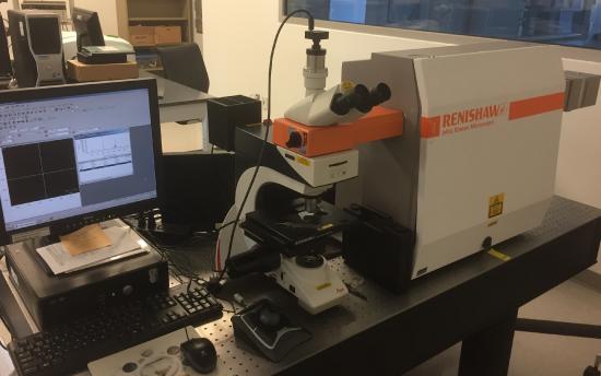 |
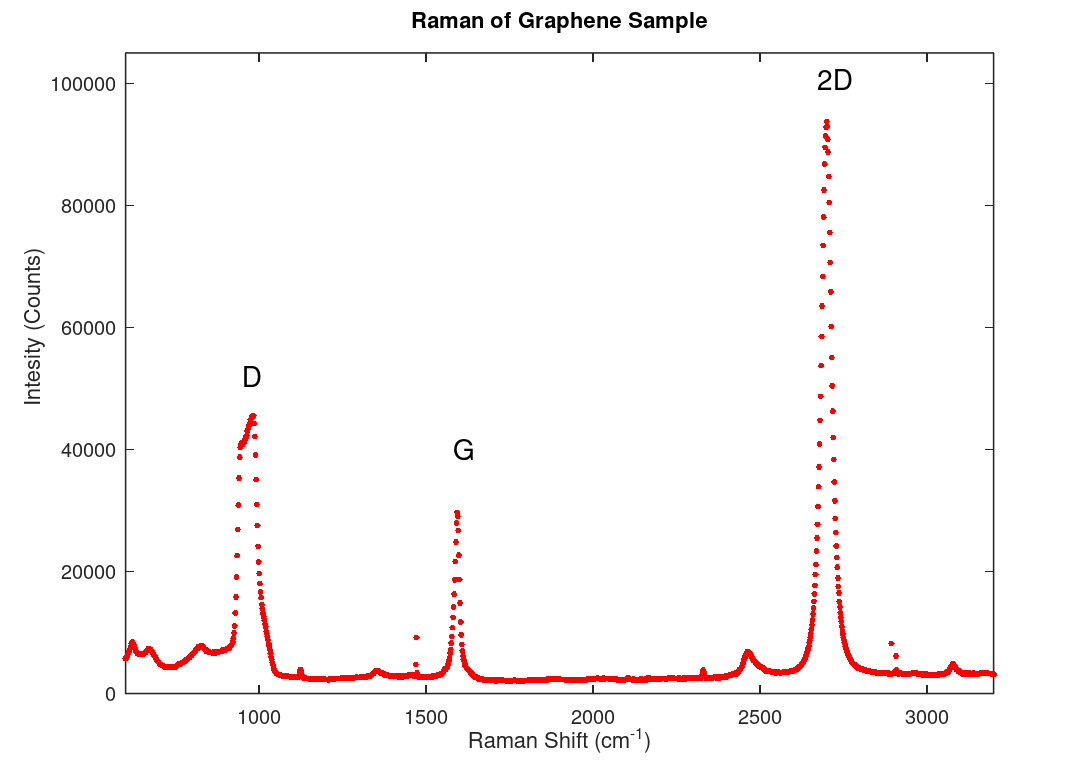 |
| Raman spectrometer with traditional microscope to position the sample and computer to run the spectrometer and to do analysis. Power and laser is behind the instrument. | Raman spectrum of a graphene sample. The G and 2D peak are typical of graphene in a Raman spectrum. Other carbon allotropes will have different Raman spectrums. |
- Theory, Modeling, and Simulation (TMS)
- New advances have been produced in the lab (real) because of simulation that were originally preformed based off new theories or ideas
- TMS is an important tool to help direct studies in nanotechnology
- Main idea is to study nanotechnology to direct how to use it better or to make new discoveries
- Theories are made into models which are then simulated
- Another factor is the need to interpret the data from nanotools
- Need models of measuring tools and the materials to understand interactions
- Main idea is to study nanotechnology to direct how to use it better or to make new discoveries
- Protocol for this "tool"
- Theory: what do we know about the materials and tools
- Model: represent the theory in a testable fashion (equations; numerical analysis techniques)
- Simulate: Test the models
- Success for known results
- Use the model to predict some new results
- Laboratory test for the new results to confirm the model
- Failure (not bugs but failure of the model)
- Re-work the model
- In rare instances look at the theory
- Success for known results
Nanotechnology involves almost everything
- Nanomaterials
- Semiconducting nanostructures
- Buckyballs
- Nanotubes
- Nanowires
- Nanoparticles (like quantum dots)
- Semiconducting nanostructures
- Nano-optics or nanophotonics
- Light and its interaction at a nanoscale
- Metamaterials (negative index of refraction among other "non-natural" properties) are the most promising here
- Nanomechanics
- Nanofluidics (study of fluids confined to a nanostructure)
- Nanobiotechnology
Additional websites to satiate your curiosity on nanotechnology
- https://www.nano.gov
- https://www.nature.com/nnano/ - Nature Magazine's Nanotechnology Journal
- https://www.ornl.gov/facility/cnms
- https://nanohub.org - this is for educators and researchers can be very high level
- https://nanocenter.umd.edu
- https://www.olympus-lifescience.com/en/microscope-resource/primer/java/electronmicroscopy/magnify1/ - simulation of an electron microscope
- https://www.renishaw.com/en/raman-spectroscopy--6150 - Renishaw's Raman Spectroscopy page (they have links to a lot of literature on Raman spectroscopy)
- http://mw.concord.org/modeler/ - Molecular Workbench: Simulator program for learning science in a realistic manner
- https://www.sciencenews.org - General science periodical but you can search for Nanotechnology and get interesting articles
- https://www.nanowerk.com - kinda like a warehouse of nanotechnology links (more for learning)
- https://www.graphene-info.com - kinda like a warehouse of graphene articles and links
- https://www.nationalgeographic.org/encyclopedia/nanotechnology/ - National Geographic article on Nanotechnology
- https://science.howstuffworks.com/nanotechnology.htm
- https://www.agilent.com/labs/features/2011_101_nano.html
- https://www.cdc.gov/niosh/programs/nano/default.html - CDC laboratory that investigates the safety of nanotechnology
- https://www.open-raman.org - open source Raman project so you can build your won Raman spectrometer (costs a bit, still)
- https://www.ncbi.nlm.nih.gov/pmc/articles/PMC6982820/ - An article on this history of nanotechnology that might be of interest to some
This is just a sampling of nanotechnology, a more detail look at nanotechnology will be provide in materials science class. This is the last teacher-led case study; now it is the students turn - starting in the next section.
1For a more modern version of the Powers of Ten you might want to look at the Cosmic Eye version:
Another interesting approach is the tool on AAAS' ScienceNetlink that gives more scales then just the power of 10 movie: Scale of Universe 2. Still the original movie from 1977 is still amazingly good and has music from the famous American composer, Elmer Bernstein (The Ten Commandments, Magnificent Seven,...).
2The tendency is to use grain size here but that actually means something else with regards to metallurgy so instead we will say nanoparticle size. Gold is obviously gold when we look at it, but a 30 nm nanoparticle size of gold is red. As you make larger and large nanoparticles it starts to change from red to a bluish-purple hue. The shape also can cause color change so rather than grinding it like you would in ancient times you would purposely make spheres or prismoids to get different colors (note that the sphere would be different color then prismoid if both were the same size).
3The Platonic solids were described by Plato (or, maybe, Pythagoras) and consist of five solids: the cube, tetrahedron, octahedron, icosahedron, and dodecahedron. These solids are very interesting in the field of mathematics and crystallography (and by association materials science).
4You can examine this more by using one of Scott Sinex's Material Sciences Excelets (in particular one named "Carbon Nanotube"). This, while designed for Excel, will run on LibreOffice's spreadsheet but does not work on MacOS Numbers.
5The example list of probes herein is from Bruker, a company that sells scientific equipment, in particular AFM and STM probes (Bruker probes division).