
7.11.2: Integrators
- Page ID
- 53016

The basic operation of an integrator is shown in Figure \(\PageIndex{1}\). The output voltage is the result of the definite integral of \(V_{in}\) from time = 0 to some arbitrary time \(t\). Added to this will be a constant that represents the output of the network at \(t = 0\). Remember, integration is basically the process of summation. You can also think of this as finding the “area under the curve”. The output of this circuit always represents the sum total of the input values up to that precise instant in time. Consequently, if a static value (non-zero) is used as an input, the output will continually grow over time. If this growth continues unchecked, output saturation will occur. If the input quantity changes polarity, the output may also change in polarity. Having established the basic operation of the circuit, we are left with the design realization and limitations to be worked out.
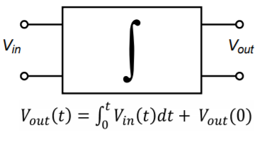
Figure \(\PageIndex{1}\): A basic integrator.
As noted in earlier work, the response of an op amp circuit with feedback will reflect the characteristics of the feedback elements. If linear elements are used, the resulting response will be linear. If a logarithmic device is used in the feedback loop, the resulting response will have a log or anti-log character. In order to achieve integration, then, the feedback network requires the use of an element that exhibits this characteristic. In other words, the current through the device must be proportional to either the integral or differential of the voltage across it. Inductors and capacitors answer these requirements, respectively. It should be possible then, to create an integrator with either an inductor or a capacitor. Capacitors tend to behave in a more ideal fashion than do inductors. Capacitors exhibit virtually no problems with stray magnetic field interference, do not have the saturation limitations of inductors, are relatively inexpensive to manufacture, and operate reliably over a wide frequency range. Because of these factors, the vast majority of integrators are made using capacitors rather than inductors. The characteristic Equation for a capacitor is
\[i(t)=C \frac{dv(t)}{dt} \label{10.1} \]
This tells us that the current charging the capacitor is proportional to the differential of the input voltage. By integrating Equation \ref{10.1}, it can be seen that the integral of the capacitor current is proportional to the capacitor voltage.
\[v(t)= \frac{1}{C}\int_{0}^{t} i(t) dt \label{10.2} \]
Assume for a moment that the capacitor voltage is the desired output voltage, as in Figure \(\PageIndex{2}\). If the capacitor current can be derived from the input voltage, the output voltage will be proportional to the integral of the input. The circuit of Figure \(\PageIndex{3}\) will satisfy our requirements. Note that it is based on the parallel-parallel inverting amplifier studied earlier. The derivation of its characteristic Equation follows.
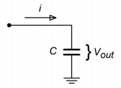
Figure \(\PageIndex{2}\): Capacitor as integration element.
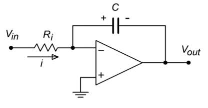
Figure \(\PageIndex{3}\): A simple op amp integrator.
First, note that the voltage across the capacitor is equal to the output voltage. This is due to the virtual ground at the inverting op amp terminal. Given the polarities marked, the capacitor voltage is of opposite polarity.
\[V_{out}(t)=−V_c (t) \label{10.3} \]
Due to the virtual ground at the op amp's inverting input, all of \(V_in\) drops across \(R_i\). This creates the input current, \(i\).
\[i(t)= \frac{V_{in} (t)}{R_i} \label{10.4} \]
Because the current drawn by the op amp's inputs is negligible, all of the input current flows into the capacitor, \(C\). Combining Equations \ref{10.2} and \ref{10.4} yields
\[V_c (t)= \frac{1}{C} \int \frac{V_{in} (t)}{R_i} dt \\ V_c (t)= \frac{1}{R_i C} \int V_{in} (t)dt \label{10.5} \]
Combining Equation \ref{10.5} with Equation \ref{10.3} produces the characteristic Equation for the circuit.
\[V_{out} (t)=− \frac{1}{R_i C} \int V_{in} (t) dt \label{10.6} \]
Note that this Equation assumes that the circuit is initially relaxed (i.e., there is no charge on the capacitor at time = 0). The only difference between Equation \ref{10.6} and the general Equation as presented in Figure \(\PageIndex{1}\) is the preceding constant \(−1/R_iC\). If the inversion or magnitude of this constant creates design problems, it can usually be corrected by gain/attenuation networks and/or inverting buffers. Finally, it is worth noting that due to the virtual ground at the inverting input, the input impedance of this circuit is approximately equal to \(R_i\), as is the case with the ordinary parallel-parallel inverting amplifier.
10.2.1: Accuracy and Usefulness of Integration
As long as the circuit operation follows the model presented above, the accuracy of Equation \ref{10.6} is very high. Small errors occur due to the approximations made. One possible source is the op amp's input bias current. If the input signal current is relatively low, the idealization that all of the input current will bypass the op amp and flow directly into the capacitor is no longer realistic. One possible solution is to use an FET input op amp. The limited frequency response and noise characteristics of the op amp will also play a role in the ultimate circuit accuracy. Generally, slew rate performance is not paramount, as integrators tend to “smooth out” signal variations. As long as the input signal stays within the op amp's frequency limits, well above the noise floor, and the output does not saturate, accurate integration results.
Circuits of this type can be used to model any number of physical processes. For example, the heat stress on a given transducer might be found by integrating the signal across it. The resulting signal could then be compared to a predetermined maximum. If the temperature proved to be too high, the circuit could be powered down as a safety measure. Although the initial reaction might be to directly measure the temperature with some form of thermal sensor, this is not always practical. In such a case, simulation of the physical process is the only reasonable route.
10.2.2: Optimizing the Integrator
For best performance, high-quality parts are a must. Low offset and drift op amps are needed, as the small DC values that they produce at the input will eventually force the circuit into saturation. Although they are not shown in Figure \(\PageIndex{3}\), bias and offset compensation additions are usually required.
Very low offset devices such as chopper-stabilized (or commutating auto-zero) op amps may be used for lower frequency applications. For maximum accuracy, a small input bias current is desired, and thus, FET input op amps should be considered. Also, the capacitor should be a stable, low-leakage type, such as polypropylene film. Electrolytic capacitors are generally a poor choice for these circuits.
Even with high-quality parts, the basic integrator can still prove susceptible to errors caused by small DC offsets. The input offset will cause the output to gradually move towards either positive or negative saturation. When this happens, the output signal is distorted, and therefore, useless. To prevent this it is possible to place a shorting switch across the capacitor. This can be used to re-initialize the circuit from time to time. Although this does work, it is hardly convenient. Before we can come up with a more effective cure, we must first examine the cause of the problem.
We can consider the circuit of Figure \(\PageIndex{3}\) to be a simple inverting amplifier, where \(R_f\) is replaced by the reactance of the capacitor, \(X_C\). In this case, we can see that the magnitude of the voltage gain is
\[A_v=− \frac{X_C}{R_i} =− \frac{1}{2\pi f C R_i} \nonumber \]
Because \(X_C\) is frequency-dependent, it follows that the voltage gain must be frequency-dependent. Because \(X_C\) increases as the frequency drops, the voltage gain must increase as the frequency decreases. To be more specific, the gain curve will follow a −6 dB per octave slope. Eventually, the amplifier's response reaches the open-loop response. This is shown in Figure \(\PageIndex{4}\).
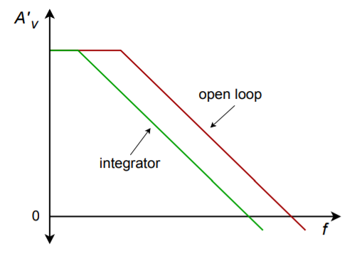
Figure \(\PageIndex{4}\): Response of a simple integrator.
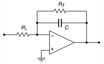
Figure \(\PageIndex{5}\): A practical integrator.
The DC gain of the system is at the open loop-level, thus it is obvious that even very small DC inputs can play havoc with the circuit response. If the low-frequency gain is limited to a more modest level, saturation problems can be reduced, if not completely eliminated. Gain limiting may be produced by shunting the integration capacitor with a resistor, as shown in Figure \(\PageIndex{5}\). This resistor sets the upper limit voltage gain to
\[A_{max}=− \frac{R_f}{R_i} \nonumber \]
As always, there will be a trade-off with modification. By definition, integration occurs where the amplitude response rolls off at −6 dB per octave, as this is the response of our idealized capacitor model. Any alteration to the response curve will impact the ultimate accuracy of the integration. By limiting the low frequency gain, the Bode amplitude response will no longer maintain a constant −6 dB per octave rolloff. Instead, the response will flatten out below the critical frequency set by \(C\) and \(R_f\), as shown in Figure \(\PageIndex{6}\). This critical frequency, \(f_{low}\), is found in the standard manner,
\[f_{low} = \frac{1}{2\pi R_f C} \label{10.7} \]
This is a very important frequency. It tells us where the useful integration range starts. If the input frequency is less than \(f_{low}\), the circuit acts like a simple inverting amplifier and no integration results. The input frequency must be higher than \(f_{low}\) for useful integration to occur. The question then, is how much higher? A few general rules of thumb are useful. First, if the input frequency equals \(f_{low}\), the resulting calculation will only be about 50% accurate1. This means that significant signal amplitude and phase changes will exist relative to the ideal. Second, at about 10 times \(f_{low}\), the accuracy is about 99%. At this point, the agreement between the calculated and actual measured values will be quite solid.
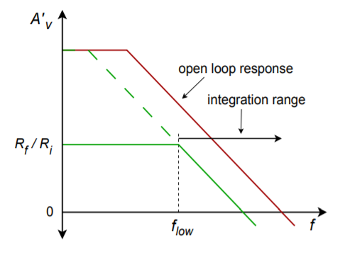
Figure \(\PageIndex{6}\): Response of a practical integrator.
Example \(\PageIndex{1}\)
Determine the Equation for \(V_{out}\), and the lower frequency limit of integration for the circuit of Figure \(\PageIndex{7}\).
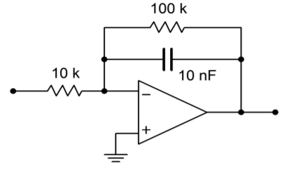
Figure \(\PageIndex{7}\): Integrator for Example \(\PageIndex{1}\).
The general form of the output Equation is given by Equation \ref{10.6}.
\[V_{out}(t)=− \frac{1}{R_iC} \int V_{in} (t) dt \\ V_{out}(t)=− \frac{1}{10 \text{ k}\times 10 \text{ nF}}\int V_{in} (t) dt \\ V_{out}(t)=−10^4\int V_{in} (t) dt \nonumber \]
The lower limit of integration is set by \(f_{low}\).
\[f_{low} = \frac{1}{2\pi R_f C} \\ f_{low} = \frac{1}{2 \pi 100 \text{ k}\times 10 \text{ nF}} \\ f_{low} =159 \text{ Hz} \nonumber \]
This represents our 50% accuracy point. For 99% accuracy, the input frequency should be at least one decade above \(f_{low}\), or 1.59 kHz. Accurate integration will continue to higher and higher frequencies.
The upper limit to useful integration is set by two factors: the frequency response of the op amp, and the signal amplitude versus noise. Obviously, at much higher frequencies, the basic assumptions of the circuit's operation will no longer be valid. The use of wide-bandwidth op amps reduces this limitation but cannot eliminate it. All amplifiers will eventually reach an upper frequency limit. Perhaps not so obvious is the limitation caused by signal strength. As noted earlier, the response of the integrator progresses at −6 dB per octave, which is equivalent to −20 dB per decade. In other words, a tenfold increase in input frequency results in a tenfold reduction in output amplitude. For higher frequencies, the net attenuation can be very great. At this point, the output signal runs the risk of being lost in the output noise. The only way around this is to ensure that the op amp is a low-noise type, particularly if a wide range of input frequencies will be used. For integration over a narrow band of frequencies, the RC integration constant may be optimized to prevent excessive loss.
Now that we have examined the basic structure of the practical integrator, it is time to analyze its response to different input waveforms. There are two basic ways of calculating the output: time-continuous or time-discrete. The time-continuous method involves the use of the indefinite integral, and is well suited for simple sinusoidal inputs. Waveforms that require a more complex time domain representation, such as a square wave, may be analyzed with the time-discrete method. This corresponds to the definite integral.
10.2.3: Analyzing Integrators with the Time-Continuous Method
The time-continuous analysis approach involves finding a time-domain representation of the input waveform and then inserting it into Equation \ref{10.6}. The indefinite integral is taken, and the result is the time-domain representation of the output waveform. The constant term produced by the indefinite integral is ignored. As long as the input waveform can be written in a time-domain form, this method may be used. Although any waveform may be expressed in this way, it is not always practical or the most expedient route. Indeed, relatively common waveforms such as square waves and triangle waves require an infinite series time-domain representation. We shall not deal with these waveforms in this manner. The time-continuous integration of these functions is left as an exercise in the Challenge Problems at the end of this chapter.
Example \(\PageIndex{2}\)
Using the circuit of Figure \(\PageIndex{7}\), determine the output if the input is a 1 V peak sine wave at 5 kHz. First, write the input signal as a function time.
\[V_{in} (t)=1 \sin 2 \pi 5000t \nonumber \]
Substitute this input into Equation \ref{10.6}:
\[V_{out}(t) = − \frac{1}{R_iC} \int V_{in} (t) dt \\ V_{out}(t) = − \frac{1}{10 \text{ k}\times 10 \text{ nF}} \int 1 \sin 2 \pi 5000t dt \\ V_{out}(t) = −10^4 \int 1 \sin 2 \pi 5000t dt \\ V_{out}(t) = -10^{4} \frac{1}{2 \pi 5000t} \int 2 \pi 5000t \sin 2 \pi 5000t dt \\ V_{out}(t) = -0.318 (- \cos 2 \pi 5000 t) \\ V_{out}(t) = 0.318 \cos 2 \pi 5000 t \nonumber \]
Thus, the output is a sinusoidal wave that is leading the input by 90\(^{\circ}\) and is 0.318 V peak. Again, note that the constant produced by the integration is ignored. In Example 1 it was noted that \(f_{low}\) for this circuit is 159 Hz. Because the input frequency is over 10 times \(f_{low}\), the accuracy of the result should be better than 99%. Note that if the input frequency is changed, both the output frequency and amplitude change. For example, if the input were raised by a factor of 10 to 50 kHz, the output would also be at 50 kHz, and the output amplitude would be reduced by a factor of 10, to 31.8 mV. The output would still be a cosine, though.
Computer Simulation
Figure \(\PageIndex{8}\) shows the Multisim simulation of the circuit of Example \(\PageIndex{2}\). The steady-state response is graphed in Figure \(\PageIndex{8b}\)..
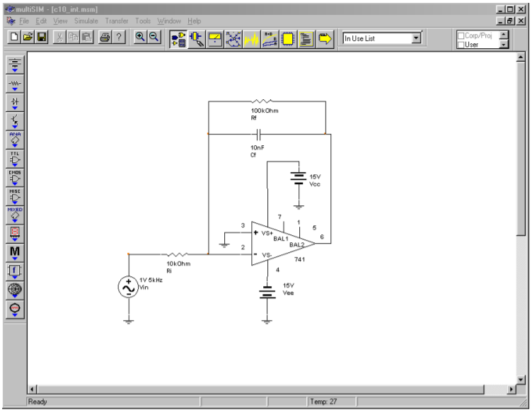
Figure \(\PageIndex{8a}\): Integrator in Multisim.
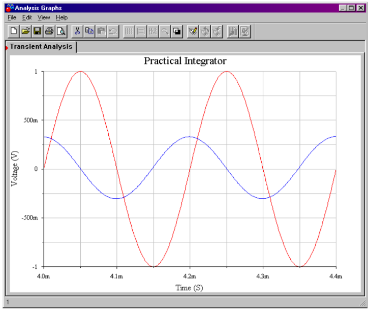
Figure \(\PageIndex{8b}\): Integrator input and output waveforms.
Note that in order to achieve steady-state results, the output is plotted only after several cycles of the input have passed through. Even after some 20 cycles, the output is not perfectly symmetrical. In spite of this, the accuracy of both the amplitude and phase is quite good when compared to the calculated results. This further reinforces the fact that the circuit is operating within its useful range. It can be instructive to rerun the simulation to investigate the initial response as well.
10.2.4: Analyzing Integrators with the Time-Discrete Method
Unlike the time-continuous approach, this method uses the definite integral and is used to find an output level at specific instances in time. This is useful if the continuous time-domain representation is somewhat complex, and yet the wave shape is relatively simple, as with a square wave. Often, a little logic may be used to ascertain the shape of the resulting wave. The integral is then used to determine the exact amplitude. The time-discrete method also proves useful for more complex waves when modeled within a computer program. Here, several calculations may be performed per cycle, with the results joined together graphically to form the output signal.
The basic technique revolves around finding simple time-domain representations of the input for specific periods of time. A given wave might be modeled as two or more sections. The definite integral is then applied over each section, and the results joined.
Example \(\PageIndex{3}\)
Sketch the output of the circuit shown in Figure \(\PageIndex{7}\) if the input signal is a 10 kHz, 2 V peak square wave with no DC component.
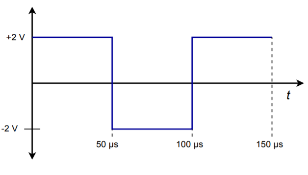
Figure \(\PageIndex{9}\): Input waveform for Example \(\PageIndex{3}\).
The first step is to break down the input waveform into simple-to-integrate components and ascertain the basic shape of the result. The input is sketched in Figure \(\PageIndex{9}\). The input may be broken into two parts: a non-changing 2 V potential from 0 to 50 \(\mu\)s, and a non-changing −2 V potential from 50 \(\mu\)s to 100 \(\mu\)s. The sequence repeats after this.
\[V_{in} (t) = 2 \text{ from } t=0, \text{ to } t=50 \mu s \\ V_{in} (t)= − 2 \text{ from } t=50 \mu s, \text{ to } t=100 \mu s \nonumber \]
In essence, we are saying that the input may be treated as either \(\pm\)2 V DC for short periods of time. Because integration is a summing operation, as time progresses, the area swept out from underneath the input signal increases, and then decreases due to the polarity changes. It follows that the output will grow (or shrink) in a linear fashion, as the input is constant. In other words, straight ramps will be produced during these time periods. The only difference between them will be the polarity of the slope. From this we find that the expected output waveform is a triangle wave. All we need to do now is determine the peak value of the output. To do this, perform the definite integral using the first portion of the input wave.
\[ V_{out}(t)= − \frac{1}{R_iC} \int V_{in} (t) dt \\ V_{out}(t) = − \frac{1}{10 \text{ k} \times 10 \text{ nF}} \int_{0}^{50\mu s} 2 dt \\ V_{out}(t) = −10^4 \times 2 \times \left. t\right|_{t=0}^{t=50 \mu s} \\ V_{out}=−20000 \times 50 \mu s \\ V_{out}=−1V \nonumber \]
This represents the total change over the 50 \(\mu\)s half-cycle interval. This is a peak-to-peak change, saying that the output is 1 V negative relative to its value at the end of the preceding half-cycle. Integration for the second half cycle is similar, and produces a positive change. The resulting waveform is shown in Figure \(\PageIndex{10}\).
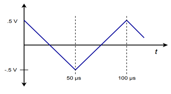
Figure \(\PageIndex{10}\): Output waveform for Example \(\PageIndex{3}\).
Note that the wave is effectively inverted. For positive inputs, the output slope is negative. Because the input frequency is much higher than \(f_{low}\), we can once again expect high accuracy. Although the solution seems to imply that the output voltage should swing between 0 and −1 V, a real world integrator does indeed produce the indicated \(\pm\) 0.5 V swing. This is due to the fact that the integration capacitor in this circuit will not be able to maintain the required DC offset indefinitely.
Example \(\PageIndex{4}\)
Figure \(\PageIndex{11a}\) shows an integrator connected to an accelerometer. This device produces a voltage that is proportional to the acceleration it experiences2. Accelerometers may be fastened to a variety of physical devices in order to determine how the devices respond to various mechanical inputs. This would be useful, for example, in experimentally determining the mechanical resonance characteristics of a surface. Another possibility is the determination of the lateral acceleration of an automobile as it travels through a corner. By integrating this signal, it is possible to determine velocity, and a further integration will produce position. If the accelerometer produces the voltage shown in Figure \(\PageIndex{11}\), determine the shape of the velocity curve (assume a non-repetitive input wave).
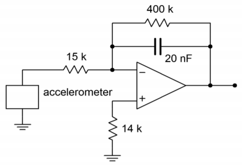
Figure \(\PageIndex{11a}\): Accelerometer with integrator circuit.
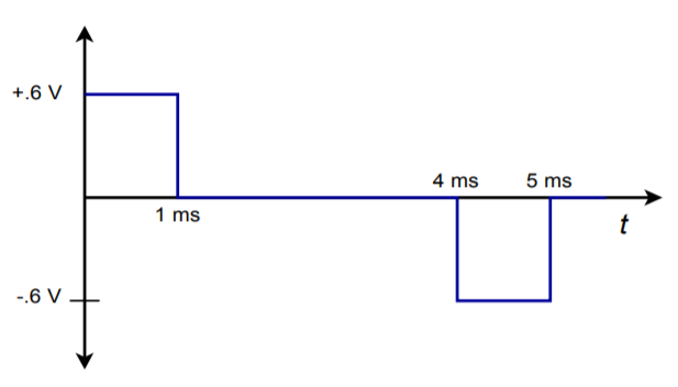
Figure \(\PageIndex{11b}\): Signal produced by accelerometer.
First, check the frequency limit of the integrator in order to see if high accuracy may be maintained. If the input waveform was repetitive, it would be approximately 200 Hz (1/ 5 ms).
\[f_{low} = \frac{1}{2 \pi R_f C} \\ f_{low} = \frac{1}{2 \pi 400 \text{ k} \times 20 \text{ nF}} \\ f_{low} = 19.9 \text{ Hz}\nonumber \]
The input signal is well above the lower limit. Note that the input waveshape may be analyzed in piece-wise fashion, as if it were a square wave. The positive and negative portions are both 1 ms in duration, and 0.6 V peak. The only difference is the polarity. As these are square pulses, we expect ramp sections for the output. For the positive pulse (\(t = 0\) to \(t =1\) ms),
\[ V_{out}(t)= − \frac{1}{R_iC} \int V_{in} (t) dt \\ V_{out}(t) = − \frac{1}{15 \text{ k} \times 20 \text{ nF}} \int_{0}^{10^{-3}} .6 dt \\ V_{out}(t) = -3333 \times 0.6 \times \left. t\right|_{t=0}^{t=10^{-3}} \\ V_{out} = −2000 \times 10^{−3} \\ V_{out} = −2 V \nonumber \]
This tells us that we will see a negative going ramp with a −2 V change. For the time period between 1 ms and 4 ms, the input signal is zero, and thus the change in output potential will be zero. This means that the output will remain at −2 V until \(t = 4\) ms.
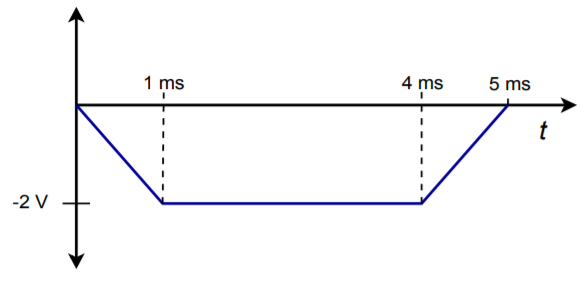
Figure \(\PageIndex{12}\): Integrator output.
For the period between 4 ms and 5 ms, a positive going ramp will be produced. Because only the polarity is changed relative to the first pulse, we can quickly find that the change is \(+2\) V. The input waveform is nonrepetitive, so the output waveform appears as shown in Figure \(\PageIndex{12}\). (A repetitive input would naturally cause the integrator to “settle” around ground over time, producing the same basic waveshape, but shifted positively.) This waveform tells us that the velocity of the device under test increases linearly up to a point. After this point, the velocity remains constant until a linear decrease in velocity occurs. (Remember, the integrator inverts the signal, so the output curve is effectively upside down. If the input wave indicates an initial positive acceleration, the actual output is an initial positive velocity.) On a different time scale, these are the sort of waveforms that might be produced by an accelerometer mounted on an automobile that starts at rest, smoothly climbs to a fixed speed, and then smoothly brakes to a stop.
References
1The term 50% accurate is chosen for convenience. The actual values are 50% of the calculated for power and phase angle and 70.7% of calculated for voltage
2A mechanical accelerometer consists of a small mass, associated restoring springs, and some form of transducer that is capable of reading the mass's motion. More recent designs may be fashioned using micro-machined chips, where the deflection of a mass-supporting beam is measured indirectly.