
7.4.4: Internal Photoelectric Effect in Semiconductors
- Page ID
- 85124
As noted, there is not chance to observe internal photoelectric effects in metals. The concentration of mobile electrons in metals is very high, of the order of \( 10^{21} - 10^{22} \) per one cubic centimeter. A relatively small number of photoelectrons generated inside the metal would not change it properties in an observable way.
But in semiconductors the situation may be quite different. Think of a pure semiconductor material, such as that shown in the Fig. 7.15. Essentially, all electrons in such crystals are “employed” in forming the covalent interatomic bonds. In order to “rip out” an electron from a bond some energy \( Phi \) is needed (in analogy to the energy needed to eject an electron from a metal in the external photoelectric effect). But no such energy is available – so, effectively, the electrons are “immobilized”, none are available to carry electric current across the crystal.
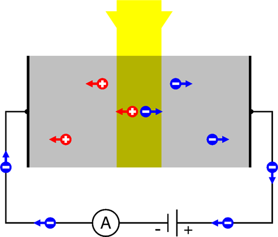
But the situation may change if the crystal is illuminated by photons of energy \( hf \) higher than \( \Phi \). Then, the internal photoelectric effect may occur. And if an electron is “knocked out” of a covalent bond, it leaves behind an incomplete binding – which is nothing else that a hole. In other words, what happens is that a photon disappears, but in the process it creates a pair – an electron, and a hole. And both can migrate away from the spot where the event took place.
The effect can be detected, if we apply voltage across the crystal using two metal electrodes attached to opposite crystal sites. It’s shown schematically in the Fig. \(\PageIndex{1}\). The electrons and the holes are pulled in opposite directions: the negative electrons migrate towards the positive electrode, and the positive holes towards the negative electrode. The electrons can enter the electrode and then can flow down the wire to the voltage source (the battery) – and then1, through the ammeter to the negative electrode. Here the electrons meet the holes flowing from inside the crystal. Holes cannot flow down a metal wire – so they recombine with the electrons. A recombination is an opposite process as compared with the pair creation2.
The current flowing in the circuit (referred to as the photocurrent ) can be measured by a sensitive ammeter. It is proportional to the intensity of the incident light – and therefore such a method of internal photoelectric effect detection is used – e.g., by photographers – for measuring light intensity in simple devices called “photometers”. Most often, The semiconducting material used in inexpensive photometers of such type is Cadmium Sulfide (CdS) – such CdS “photoelements” could be purchased in Radio Shack stored when they still existed, and people used them to build their own amateur light intensity detectors. Why CdS? Because the Φ value in it is exceptionally low, so the internal photoelectric effect may occur in this material for low-energy photons, such as those of red light or of infrared light.
1.Let’s keep in mind that electric current never can enter a battery and to “stay inside”. The battery acts like a pump, it only “pulls in” electron through one terminal, and makes the same number of electrons to leave through the other terminal. A “voltage source” is not a source of electron, it only “energizes” electrons passing through it.
2. A photon creates an electron-hole pair, and disappears. An opposite process may be a “mirror image”: a hole and an electron meet and “re-recreate” the covalent bond, and the energy released in the process “re-creates” a photon. This is called a radiative recombination, and such a process occurs in the well-known light emitting diodes (LEDs). However, more often the recombination is non-radiative, the energy released by the recombining pair is “utilized” in a different way by the crystal.