
7.4.3: The p-n Junction
- Page ID
- 85123
Suppose that a Si crystal plate is p-type on one side, and n-type on the other, and at some depth below the surface the two types get in contact – what’s created then is a so-called p-n junction (some people prefer calling it n-p junction, which is essentially the same). The interface area should be very thin, with thickness of the order of 1 micrometer or less. Such p-n junctions play extremely important roles in modern semiconductor electronics. Any piece of modern electronics, such as a cellphone, a PC, or the GPS in your car, they all contain millions of p-n junctions. The p-n junction is also the “heart” of every PV solar power converter.
Let’s first discuss what happens to the loose electrons and holes roaming around in the n-type and p-type areas on both sides of the p-n junction. They exhibit a tendency of doing the same as any particles suspended in any kind of medium normally do – namely, of diffusing, or spreading over a larger and larger area. This tendency is limited by the crystal boundaries – the only possible direction is across the p-n interface. And so they do!
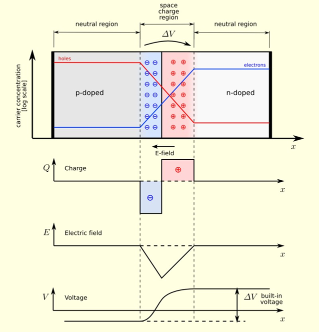
To explain the effects occurring in p-n junction we will use a concise version of the explanation outlined in a Wikipedia article, as well as an instructive graph from this article, copied into the Fig. \(\PageIndex{1}\). The physical process that determines the properties of a p-n junction is diffusion: some electrons from the n-type block penetrate some distance into the p-type block – and vice versa: some holes from the p-type block penetrate some distance into the n-type block. As noted, the p-type and the n-type materials are normally electrically neutral – so, due to the hole diffusion, a positive electric charge is accumulated on the right side of the p n interface; and due to the diffusion of electrons, a negative charge accumulates on the left side of the interface, as shown in the Q-plot in the Fig. \(\PageIndex{1}\). The existence of regions of opposite electric charges, some distance apart, gives rise to an electric field, pointing in the direction from the positive region towards the negative region. The magnitude of the E field as a function of x is shown in the E-plot in the figure. Note it’s always negative – it’s because the field vector is pointing to the left, which is the “negative” direction in the graph.
The last plot in the Fig. \(\PageIndex{1}\) shows the electric potential as the function of \( x \). If there is an electric field parallel to the \( x \) direction, there is always electric potential difference between two different points, \( x_1 \) and \( x_2 \). The basic relation between the magnitude of electric field parallel to the \( x \) axis and the \( x \)-dependent potential \( V(x) \) is:
\[ E=-\frac{d V}{d x} \]
Hence, the potential difference - commonly referred to as the voltage - can be obtained by integrating:
\[ V\left(x_{2}\right)-V\left(x_{1}\right)=-\int_{x_{1}}^{x_{2}} E(x) d x \]
The \(E(x)\) function in the present case is a triangle, and it's easy to show that an integral over such triangle function is of the shape of a "rounded step", as shown in the last plot in the Fig. \(\PageIndex{1}\).
The potential step existing in the \(p \rightarrow n\) junction is commonly referred to as the "built-in voltage". And this voltage step is exactly what allows a \( pn \) junction to act as a converter of solar energy to electric power. But to explain how exactly such conversion happens, we should return for a moment to the internal photoelectric effect.