3.3.3: Doped Semiconductors
- Page ID
- 89948

To see how we can make silicon a useful electronic material, we will have to go back to its crystal structure. Suppose that somehow (and we will talk about how this is done later) we could substitute a few atoms of phosphorus for some of the silicon atoms.
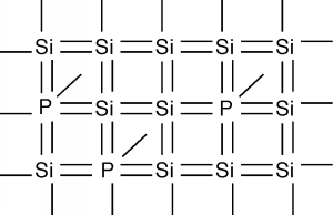
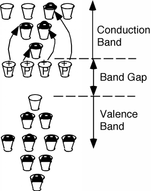
If you sneak a look at the periodic table, you will see that phosphorus is a group V element, as compared with silicon which is a group IV element. What this means is the phosphorus atom has five outer or valence electrons, instead of the four which silicon has. In a lattice composed mainly of silicon, the extra electron associated with the phosphorus atom has no "mating" electron with which it can complete a shell, and so is left loosely dangling on the phosphorus atom, with relatively low binding energy. In fact, with the addition of just a little thermal energy (from the natural or latent heat of the crystal lattice) this electron can break free and be left to wander around the silicon crystal. In our "energy band" picture, we have something like what we see in Figure \(\PageIndex{2}\). The phosphorus atoms are represented by the added cups with P's on them. They are new allowed energy levels which are formed within the "band gap" near the bottom of the first empty band. They are located close enough to the empty (or "conduction") band that the electrons which they contain are easily excited up into the conduction band. There, they are free to move about and contribute to the electrical conductivity of the sample. Note also, however, that since the electron has left the vicinity of the phosphorus atom, there is now one more proton than there are electrons at the atom, and hence it has a net positive charge of +1 \(q\). We have represented this by putting a little "+" sign in each P-cup. Note that this positive charge is fixed at the site of the phosphorous atom called a donor since it "donates" an electron up into the conduction band, but the phosphorous atom is not free to move about in the crystal.
How many phosphorus atoms do we need to significantly change the resistance of our silicon? Suppose we wanted our 1 mm by 1 mm square sample to have a resistance of one ohm as opposed to more than \(60 \mathrm{~M} \Omega\). Turning the resistance equation around we get \[\begin{array}{l} \sigma &= \ \dfrac{L}{RA} \\ &= \ \dfrac{1 \ \Omega}{1 \times 0.1^{2}} \\ &= \ 100 \ \frac{\Omega^{-1}}{\mathrm{cm}} \end{array} \nonumber \]
And hence (if we continue to assume an electron mobility of \(1000 \ \frac{\mathrm{cm}^2}{\mathrm{volt} \cdot \mathrm{sec}}\)) we get: \[\begin{array}{l} n &= \ \dfrac{\sigma}{q \mu} \\ &= \ \dfrac{100}{\left(1.6 \times 10^{-19}\right) 1000} \\ &= \ 6.25 \times 10^{17} \ \mathrm{cm}^{3} \end{array} \nonumber \]
Now adding more than \(6 \times 10^{17}\) phosphorus atoms per cubic centimeter might seem like a lot of phosphorus, until you realize that there are almost \(10^{24}\) silicon atoms in a cubic centimeter and hence only one in every 1.6 million silicon atoms must be replaced with a phosphorus atom to reduce the resistance of the sample from several 10s of Megaohms down to only one Ohm. This is the real power of semiconductors. You can make dramatic changes in their electrical properties by the addition of only minute amounts of impurities. This process is called "doping" the semiconductor. It is also one of the great challenges of the semiconductor manufacturing industry, for it is necessary to maintain fantastic levels of control of the impurities in the material in order to predict and control their electrical properties.
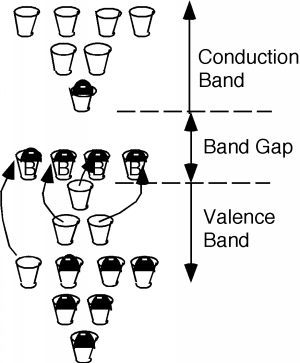
Again, if this were the end of the story, we still would not have any calculators, stereos or "Agent of Doom" video games (or at least they would be very big and cumbersome and unreliable, because they would have to work using vacuum tubes!). We now have to focus on the few "empty" spots in the lower, almost full band (Called the valence band.) We will take another view of this band, from a somewhat different perspective. I must confess at this point that what I am giving you is even further from the way things really work. The problem is, that in order to do things right, we have to get involved in momentum phase-space, a lot more quantum mechanics, and generally a bunch of math and concepts we don't really need in order to have some idea of how semiconductor devices work. What follow below is really intended as a motivation, so that you will have some feeling that what we state as results, is actually reasonable.
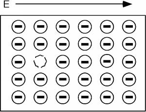
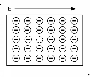
Consider Figure \(\PageIndex{3}\). Here we show all of the electrons in the valence, or almost full band, and for simplicity show one missing electron. Remeber, electrons in the valence band are bound to an atom: they can't move far. Let's apply an electric field, as shown by the arrow in the figure. The field will try to move the (negatively charged) electrons to the left, but since the band is almost completely full, the only one that can move is the one right next to the empty spot, or hole as the empty spot is called.
One thing you may be worrying about is what happens to the electrons at the ends of the sample. This is one of the places where we are getting a somewhat distorted view of things, because we should really be looking in momentum, or wave-vector space rather than "real" space. In that picture, they magically drop off one side and "reappear" on the other. This doesn't happen in real space of course, so there is no easy way we can deal with it.
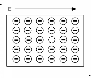
A short time after we apply the electric field we have the situation shown in Figure \(\PageIndex{4}\), and a little while after that we have Figure \(\PageIndex{5}\). We can interpret this motion in two ways. One is that we have a net flow of negative charge to the left, or if we consider the effect of the aggregate of all the electrons in the band (which we have to do because of quantum mechanical considerations beyond the scope of this book) we could picture what is going on as a single positive charge, moving to the right. This is shown in Figure \(\PageIndex{6}\). Note that in either view we have the same net effect in the way the total net charge is transported through the sample. In the mostly negative charge picture, we have a net electron flow (negative charge) to the left. In the single positive charge picture, we have a net flow of positive charge to the right. Both give the same sign for the current!
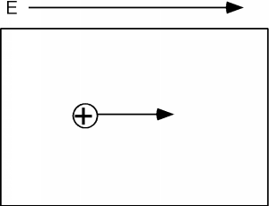
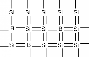
Thus, it turns out, we can consider the consequences of the empty spaces moving through the coordinated motion of electrons in an almost full band as being the motion of positive charges, moving wherever these empty spaces happen to be. We call these charge carriers "holes" and they too can add to the total conduction of electricity in a semiconductor. Using \(\rho\) to represent the density (in \(\mathrm{cm}^{-3}\)) of spaces in the valence band and \(\mu_{e}\) and \(\mu_{h}\) to represent the mobility of electrons and holes respectively (they are usually not the same) we can modify Equation \(1.1.11\) to give the conductivity \(\sigma\) when both electrons' holes are present: \[\sigma = nq \mu_{e} + \rho q \mu_{h} \nonumber \] How can we get a sample of semiconductor with a lot of holes in it? What if, instead of phosphorus, we dope our silicon sample with a group III element, such as boron? This is shown in Figure \(\PageIndex{7}\). Now we have some missing orbitals, or places where electrons could go if they were around. This modifies our energy picture as follows in Figure \(\PageIndex{8}\). Now we see a set of new levels introduced by the boron atoms. They are located within the band gap, just a little way above the top of the almost full, or valence band. Electrons in the valence band can be thermally excited up into these new allowed levels, creating empty states, or holes, in the valence band. The excited electrons are stuck at the boron atom sites called acceptors, since they "accept" an electron from the valence band, and hence act as fixed negative charges, localized there.
A semiconductor which is doped predominantly with acceptors is called p-type, and most of the electrical conduction takes place through the motion of holes. A semiconductor which is doped with donors is called n-type, and conduction takes place mainly through the motion of electrons. In n-type material, we can assume that all of the phosphorous atoms, or donors, are fully ionized when they are present in the silicon structure. Since the number of donors is usually much greater than the native, or intrinsic electron concentration, (\(\approx \left(10^{10} \mathrm{~cm}^{-3} \right)\)), if \(N_{d}\) is the density of donors in the material, then \(n\), the electron concentration, \(\approx \left(N_{d}\right)\).
If an electron deficient material such as boron is present, then the material is called p-type silicon, and the hole concentration is just \(p \simeq N_{a}\), where \(N_{a}\) is the concentration of acceptors, since these atoms "accept" electrons from the valence band.
If both donors and acceptors are in the material, then which ever one has the higher concentration wins out. (This is called compensation.) If there are more donors than acceptors then the material is n-type and \(n \simeq N_{d} - N_{a}\). If there are more acceptors than donors then the material is p-type and \(p \simeq N_{a} - N_{d}\). It should be noted that in most compensated material, one type of impurity usually has a much greater (several order of magnitude) concentration than the other, and so the subtraction process described above usually does not change things very much, e.g., \(10^{18}-10^{16} \simeq 10^{18}\).
One other fact which you might find useful is that, again, because of quantum mechanics, it turns out that the product of the electron and hole concentration in a material must remain a constant. This concept is a "mass action law" which you might be familiar with from chemistry. In silicon at room temperature: \[np \equiv n_{i}^{\ 2} \simeq 10^{20} \mathrm{~cm}^{-6} \nonumber \] Thus, if we have an n-type sample of silicon doped with \(10^{17}\) donors per cubic centimeter, then \(n\), the electron concentration is just \(10^{17}\) and \(p\), the hole concentration, is \(\frac{10^{20}}{10^{17}} = 10^{-3} \mathrm{~cm}^{3}\). The carriers which dominate a material are called majority carriers, which would be the electrons in the above example. The other carriers are called minority carriers (the holes in the example), and while \(10^{3}\) might not seem like much compared to \(10^{17}\) the presence of minority carriers is still quite important and can not be ignored. Note that if the material is undoped, then it must be that n=p=ni=1010cm-3.
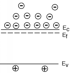
The picture of "cups" of different allowed energy levels is useful for gaining a pictorial understanding of what is going on in a semiconductor, but becomes somewhat awkward when you want to start looking at devices which are made up of both n and p type silicon. Thus, we will introduce one more way of describing what is going on in our material. The picture shown in Figure \(\PageIndex{9}\) is called a band diagram. A band diagram is just a representation of the energy as a function of position with a semiconductor device. In a band diagram, positive energy for electrons is upward, while for holes, positive energy is downwards. That is, if an electron moves upward, its potential energy increases just as with a normal mass in a gravitational field. Also, just as a mass will "fall down" if given a chance, an electron will move down a slope shown in a band diagram. On the other hand, holes gain energy by moving downward and so they have a tendency to "float" upward if given the chance - much like a bubble in a liquid. The line labeled \(E_{c}\) in Figure \(\PageIndex{9}\) shows the edge of the conduction band, or the bottom of the lowest unoccupied allowed band, while \(E_{v}\) is the top edge of the valence, or highest occupied band. The band gap, \(E_{g}\), for the material is obviously \(E_{c}-E_{v}\). The dotted line labeled \(E_{f}\) is called the Fermi level and it tells us something about the chemical equilibrium energy of the material, and also something about the type and number of carriers in the material. More on this later. Note that there is no zero energy level on a diagram such as this. We often use either the Fermi level or one or other of the band edges as a reference level on lieu of knowing exactly where "zero energy" is located.
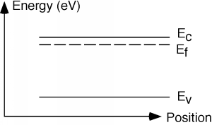
The distance (in energy) between the Fermi level and either \(E_{c}\) or \(E_{v}\) gives us information concerning the density of electrons and holes in that region of the semiconductor material. The details, once again, will have to be begged off on grounds of mathematical complexity. It turns out that you can say: \[\begin{align} n &= N_{c} e^{- \frac{E_{c}-E_{f}}{kT}} \\ p &= N_{v} e^{- \frac{E_{f}-E_{v}}{kT}} \end{align} \nonumber \] Both \(N_{c}\) and \(N_{v}\) are constants that depend on the material and temperature you are talking about, but are typically on the order of \(10^{19} \mathrm{~cm}^{-3}\). The expression in the denominator of the exponential is just Boltzman's constant, \(k\), times the temperature \(T\)of the material (in absolute temperature or Kelvin). Boltzman's constant \(k = \left(8.63 \times 10^{-5}\right) \frac{\mathrm{eV}}{\mathrm{K}}\). At room temperature \(kT = 1/40\) of an electron volt. Look carefully at the numerators in the exponential. Note first that there is a minus sign in front, which means the bigger the number in the exponent, the fewer carriers we have. Thus, the top expression says that if we have n-type material, then the conduction band must not be too far away from the Fermi level. If we have p-type material, then the valence band must be close to the Fermi level. The closer \(E_{c}\) gets to \(E_{f}\), the more electrons we have. The closer \(E_{v}\) gets to \(E_{f}\), the more holes we have. While the conduction and valence bands are seperated by a fixed band gap energy, these bands can be above or below the Fermi level. Figure \(\PageIndex{9}\) therefore must be for a sample of n-type material. Note also that if we know how heavily a sample is doped (that is, if we know what \(N_{d}\) is, for example), from the fact that \(n \simeq N_{d}\) we can use Equation \(\PageIndex{5}\) to find out how far away the Fermi level is from the conduction band: \[E_{c}-E_{f} = kT \ln \left(\frac{N_{c}}{N_{d}}\right) \nonumber \]
To help further in our ability to picture what is going on, we will often add to this band diagram, some small signed circles to indicate the presence of mobile electrons and holes in the material. Note that the electrons are spread out in energy. From our "cups" picture we know they like to stay in the lower energy states if possible, but some will be distributed into the higher levels as well. What is distorted here is the scale. The band-gap for silicon is 1.1 eV, while the actual spread of the electrons would probably only be a few tenths of an eV, not nearly as much as is shown in Figure \(\PageIndex{10}\). Let's look at a sample of p-type material, just for comparison. Note that for holes, increasing energy goes down, not up, so their distribution is inverted from that of the electrons. You can kind of think of holes as bubbles in a glass of soda or beer; they want to float to the top if they can. Note also for both n-type and p-type material there are also a few "minority" carriers, or carriers of the opposite type, which arise from thermal generation across the band-gap.