
3.3.10: LASER
- Page ID
- 89958

Speaking of lasers, what is the difference between an LED and a solid state laser? There are some differences, but both devices operate on the same principle of having excess electrons in the conduction band of a semiconductor, and arranging it so that the electrons recombine with holes in a radiative fashion, giving off light in the process. What is different about a laser? In an LED, the electrons recombine in a random and unorganized manner. They give off light by what is known as spontaneous emission, which simply means that the exact time and place where a photon comes out of the device is up to each individual electron, and things happen in a random way.
There is another way in which an excited electron can emit a photon, however. If a field of light (or a set of photons) happens to be passing by an electron in a high energy state, that light field can induce the electron to emit an additional photon through a process called stimulated emission. The photon field stimulates the electron to emit its energy as an additional photon, which comes out in phase with the stimulating field. This is the big difference between incoherent light (what comes from an LED or a flashlight) and coherent light, which comes from a laser. With coherent light, all of the electric fields associated with each phonon are all exactly in phase. This coherence is what enables us to keep a laser beam in tight focus, and to allow it to travel a large distance without much divergence or spreading out.
So how do we restructure an LED so that the light is generated by stimulated emission rather than spontaneous emission? Firstly, we build what is called a heterostructure. All this means is that we build up a sandwich of somewhat different materials, with different characteristics. In this case, we put two wide band-gap regions around a region with a narrower band gap. The most important system where this is done is the \(\mathrm{AlGaAs} / \mathrm{GaAs}\) system. A band diagram for such a setup is shown in Figure \(\PageIndex{1}\). \(\mathrm{AlGaAs}\) (pronounced "Al-Gas") has a larger band-gap then does \(\mathrm{GaAs}\). The potential "well" formed by the GaAs means that the electrons and holes will be confined there, and all of the recombination will occur in a very narrow strip. This greatly increases the chances that the carriers can interact, but we still need some way for the photons to behave in the proper manner.
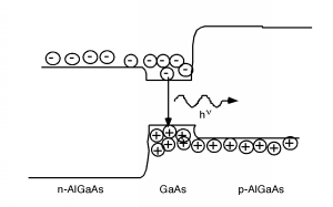
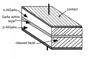
Figure \(\PageIndex{2}\) is a picture of what a real diode might look like. We have the active \(\mathrm{GaAs}\) layer sandwiched in between the two heterostructure confinement layers, with a contact on top and bottom. On either end of the device, the crystal has been "cleaved" or broken along a crystal lattice plane. This results in a shiny "mirror-like" surface, which will reflect photons. The back surface (which we can not see here) is also cleaved to make a mirror surface. The other surfaces are purposely roughened so that they do not reflect light.
Now let us look at the device from the side, and draw just the band diagram for the \(\mathrm{GaAs}\) region (Figure \(\PageIndex{3}\)). We start things off with an electron and hole recombining spontaneously. This emits a photon which heads towards one of the mirrors. As the photon goes by other electrons, however, it may cause one of them to decay by stimulated emission. The two (in phase) photons hit the mirror and are reflected and start back the other way. As they pass additional electrons, they stimulate them into a transition as well, and the optical field within the laser starts to build up.
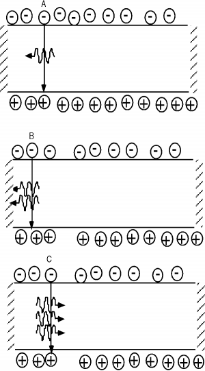
After a bit, the photons get down to the other end of the cavity. The cleaved facet, while it acts like a mirror, is not a perfect one. Some light is not reflected, but rather "leaks"; though, and so becomes the output beam from the laser. The details of finding what the ratio of reflected to transmitted light is will have to wait until later in the course when we talk about dielectric interfaces. The rest of the photons are reflected back into the cavity and continue to stimulate emission from the electrons which continue to enter the gain region because of the forward bias on the diode.
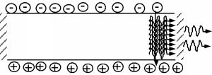
In reality, the photons do not move back and forth in a big "clump" as we have described here, rather they are distributed uniformly along the gain region. The field within the cavity will build up to the point where the loss of energy by light leaking out of the mirrors just equals the rate at which energy is replaced by the recombining electrons.