
3.4.8: Inverters and Logic
- Page ID
- 89975

As you already know, or will find out shortly, from taking a class in digital logic, logic circuits are primarily based upon a circuit called an inverter. An inverter simply takes a signal and gives you the opposite one. For instance, if a high voltage (a "one") is placed on the input of an inverter, it returns a low voltage (a "zero"). Figure \(\PageIndex{1}\) is a simple inverter based on a MOSFET transistor:
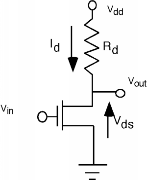 Figure \(\PageIndex{1}\): Inverter circuit
If \(V_{\text{in}}\) is zero, the MOSFET is turned off (\(V_{\text{gs}} < V_{t}\)) and so no current flows through the resistor, and \(V_{\text{out}} = V_{\text{dd}}\), a high. If \(V_{\text{in}}\) is high (and we assume that \(V_t}\) for the MOSFET is significantly less than \(V_{\text{in}}\)) then the transistor is turned on, and if \(R\) and \(\frac{W}{L}\) are chosen so that enough current flows through \(R\) to drop most of \(V_{\text{dd}}\) across it, then \(V_{\text{out}}\) will be low.
The way this is usually described is through a transfer function which tells us what the output voltage is as a function of the input voltage. Let's digress for just a minute and see how such a function can be arrived at. Looking back at Figure \(\PageIndex{2}\) it should be easy to see that \[V_{\text{dd}} = I_{d} R_{d} + V_{\text{ds}}\]
We can re-write this as an equation for \(I_{d}\). \[I_{d} = \frac{V_{\text{dd}}}{R_{d}} - \frac{V_{\text{ds}}}{R_{d}}\]
This is called a load-line equation. It says that \(I_{d}\) varies linearly with \(V_{\text{ds}}\) (with a negative slope) and has a vertical offset of \(\frac{V_{\text{dd}}}{R_{d}}\). Let's suppose we have the MOSFET transistor for which we have already plotted the characteristic curves in a previous plot. We will let \(V_{\text{dd}} = 5 \mathrm{~Volts}\), and let \(R_{d} = 1 \mathrm{~k} \Omega\). From Equation \(\PageIndex{2}\) we can see that when \(V_{\text{ds}} = 0\), \(I_{d}\) will be \(5 \mathrm{~mA}\), and when \(V_{\text{ds}} = V_{\text{dd}}\), \(I_{d}\) will be \(0\). This then gives us a straight line on the characteristic curve plot which is called the load line. This is shown in Figure \(\PageIndex{2}\).
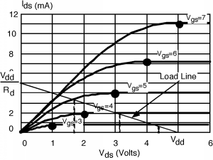
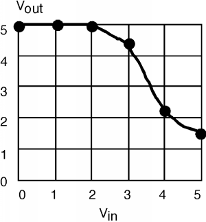
By looking back at the schematic for the inverter in Figure \(\PageIndex{1}\), we see that the same current \(I_{d}\) flows through the load resistor \(R_{d}\) and through the transistor. Thus, the correct value of current and voltage for the circuit for any given gate voltage is the simultaneous solution of the load line equation and the transistor behavior, which, of course, is just the intersection of the load line with the appropriate characteristic curve. Thus it is a simple matter of drawing vertical lines down from each \(V_{\text{in}}\) curve or \(V_{\text{gs}}\) value down to the horizontal axis to find out what the appropriate \(V_{\text{dd}}\) or output voltage will be for the inverter. Assuming that \(V_{\text{in}}\) only goes up to 5 volts, the resulting curve that we get look like Figure \(\PageIndex{3}\). This is not a great transfer characteristic. \(V_{\text{in}}\) has to get fairly large before \(V_{\text{out}}\) starts to fall, and even with the full 5-volt input, \(V_{\text{out}}\) is still greater than 1 volt. Picking a transistor with a small \(V_{t}\) and a bigger load resistor would give us a better response, but at least with this example you can see what is going on.
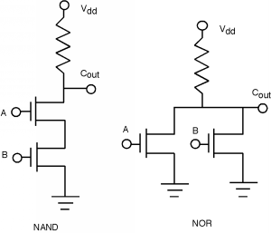
Based on this simple inverter circuit, we can build circuits which perform the NOR and NAND function. \[C_{\text{out}} = \neg \ (A+B)\]
and \[C_{\text{out}} = \neg \ (AB)\]
It should, by now, be obvious to you how the two circuits in Figure \(\PageIndex{4}\) can perform the NAND and NOR function. It turns out that with the capability to do NAND and NOR, we can build up any kind of logic function we desire.

Let's look at the inverter a little more closely. Usually, the load for the inverter will be the next stage of logic which, along with the associated interconnect wiring, we can model as a simple capacitor. The value of the capacitance will vary, but it will be on the order of \(10^{-12} \mathrm{~F}\).

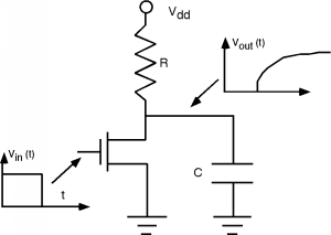
When the input to the inverter switches instantaneously to a low value, current will stop flowing through the transistor, and instead will start to charge up the load capacitance. The output voltage will follow the usual \(\mathrm{RC}\) charging curve with a time constant given just by the product of \(R\) times \(C\). If \(C\) is \(10^{-13} \mathrm{~F}\), then to get a rise time of \(1 \mathrm{~ns}\) we would have to make \(R\) about \(10^{4} \ \Omega\).
As we shall see later, it is virtually impossible to make a \(10 \mathrm{~k} \Omega\) resistor using integrated circuit techniques. Remember: \[R = \frac{\rho L}{A}\]
And thus, to get a really big resistance we need either a very tiny \(A\) (too hard to achieve and control), a really big \(L\) (takes up too much room on the chip) or a huge \(\rho\) (again, very hard to control when you get to the very low doping densities that would be required).
Even if we could find a way to build such big integrated circuit resistors, there would still be a problem. The current flowing through the resistor when the MOSFET is on would be approximately \[\begin{array}{l} I &= \frac{V}{R} \\ &= \frac{5 \mathrm{~V}}{10^{4} \ \Omega} \\ &= 5 \times 10^{-4} \mathrm{~A} \end{array}\]
This doesn't seem like much current until you consider that a Pentium II © microprocessor in about 1995 had about 6 million gates in it. This would mean a net current of \(-300 \mathrm{~Amps}\) flowing into the CPU chip! We've got to come up with a better solution, especially considering a 2022 Apple M2 microprocessor has about 20 billion gates.