
3.4.9: Transistor Loads for Inverters
- Page ID
- 89976

There are other kinds of MOSFETs besides the one we have studied so far. Strictly speaking, what we have seen up to now is called an n-channel enhancement mode MOSFET. It turns out that you can build a MOSFET which looks just like a previous figure, except that by putting some additional impurities under the gate region, we can arrange it so that there is a channel formed, even with \(V_{g} = 0\). The transistor now has a negative \(V_{t}\). The process by which the additional impurities are added is called a \(V_{t}\) adjust.
A MOSFET with a negative \(V_{t}\) can be expected to have \(I_{d} \text{-} V_{\text{ds}}\) curves similar to those for a positive \(V_{t}\) device, except for one thing. For \(V_{\text{gs}} = 0\), the device is already turned on, and so we get a usual MOSFET-type curve. Positive gate voltage turns it on even more, while negative \(V_{\text{gs}}\) tends to reduce the drain current. It takes a negative gate voltage to turn the thing off. Figure \(\PageIndex{1}\) shows comparative characteristic curves for an enhancement and depletion mode devices.
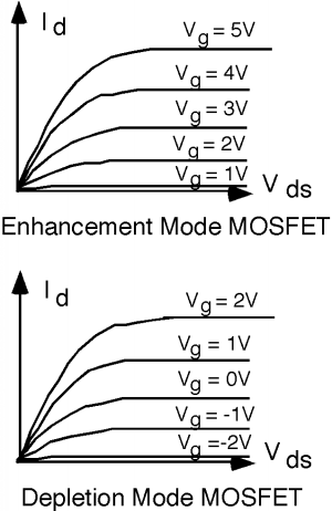
For an enhancement mode transistor, you have to get \(V_{g} > V_{t}\) (-1 Volt in this example) to enhance the conductivity or channel to make it conduct. For a depletion mode device, a gate voltage \(V_{\text{gs}}\) of \(0\), still finds the device conducting. You have to put some negative voltage on the gate to deplete the channel, in order to turn it off. We now have a depletion mode n-channel MOSFET.
How would we use a depletion mode device in an inverter gate? The answer is fairly straight-forward. In the schematic in Figure \(\PageIndex{2}\), we indicate a depletion mode MOSFET by adding a second line, under the gate, to suggest that a channel already exists in the device, even with no \(V_{g}\). Note that the gate of the depletion mode transistor (also sometimes called the pull up transistor) is connected to its source, so, in fact, \(V_{\text{gs}}\) does equal 0 for this device. The input transistor (or the pull down transistor) is just an enhancement mode MOSFET like we had before. It is not hard to choose appropriate \(W\) and \(L\) so that \(I_{\text{d sat}}\) for the pull up transistor is on the order of the \(500 \ \mu \mathrm{A}\) that we need to get our \(1 \mathrm{~ns}\) rise time on the capacitive load.
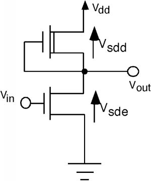
In order to get the transfer characteristic for this circuit, we first note that \[V_{\text{sdd}} = V_{\text{dd}} - V_{\text{sde}}\]
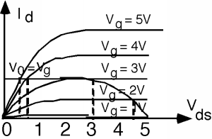
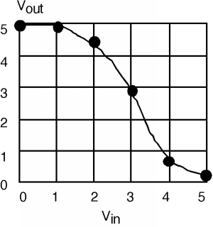
where \(V_{\text{sde}}\) is the source-drain voltage for the pull-down, or enhancement transistor, and \(V_{\text{sdd}}\), is the source-drain voltage for the depletion-mode transistor. If we want to plot the load-line for the pull-down transistor that is created by the pull-up or depletion mode transistor, we should take its \(V_{\text{gs}} = 0\) characteristic curve, shift it over by an amount \(V_{\text{dd}}\), and then reverse its polarity. When we do this we get the following shown in Figure \(\PageIndex{3}\). Noting the intersection points of the load line and the characteristic curves allows us the opportunity for drawing the transfer characteristic. This is a better looking curve. It is symmetric around the mid-voltage point, and gets closer to zero for its output "low" condition. The transition from "high" to "low" is also somewhat more abrupt, which is advantageous. Can you figure out why?
Well, we solved one problem. At least we have a pull up structure that we can manufacture. It turns out not to be too hard to build an enhancement MOSFET that has an equivalent resistance in the range we need without taking up too much chip area. We have not solved the other problem, however. We are still looking at a huge current draw for large circuits. Since on average, half of the inverter gates will be "on" in a logic circuit, we still have a large current sink to ground. This is something that would be completely prohibitive in a modern-day VLSI integrated circuit.
Fortunately, we have not run out of options for MOS structures yet.