
9.5.3: Doping
- Page ID
- 89983

Starting with a prepared, polished wafer, how do we then get an integrated circuit? We will focus on the CMOS process, described in the last chapter. Let's assume we have wafer which was doped during growth so that it has a background concentration of acceptors in it (i.e. it is p-type). Referring back to CMOS Logic, you can see that the first thing we need to build is a n-tank or moat. In order to do this, we need some way in which to introduce additional impurities into the semiconductor.
There are several ways to do this, but current technology relies almost exclusively on a technique called ion implantation. A diagram of an ion-implanter is shown in the figure in the previous section. An ion implanter uses a dopant source gas, ionizes it, and drives the ions into the wafer. The dopant gas is ionized and the resultant charged ions are accelerated through a magnetic field, where they are mass-analyzed. The vertical magnetic field causes the beam of ions to spread out, according to their mass. A thin aperture selects the ions of interest, and lets them pass, blocking all the others. This makes sure we are only implanting the ion we want, and in fact, even selects for the proper isotope! The ionized atoms are then accelerated through several tens to hundreds of kilovolts, and then deflected by an electric field, much like in an oscilloscope CRT. In fact, most of the time the ion beam is "rastered" across the surface of the silicon wafer. The ions strike the silicon wafer and pass into its interior. A measurement of the current flow in the system and its integral, is a measure of how much dopant was deposited into the wafer. This is usually given in terms of the number of dopant \(\frac{\mathrm{atoms}}{\mathrm{cm}^2}\) to which the wafer has been exposed.
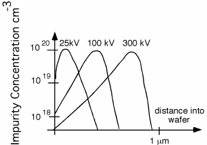
After the atoms enter the silicon, they interact with the lattice, creating defects, and slowing down until finally they stop. Typical atomic distributions, as a function of implant voltage, are shown in Figure \(\PageIndex{1}\) for implantation into amorphous silicon. When implantation is done on single crystal material, channeling the improved mobility of an ion down the "hallway" of a given lattice direction can skew the impurity distribution significantly. Just slight changes of less than a degree can make big differences in how the impurity atoms are finally distributed in the wafer. Usually, the operator of the implant machine purposely tilts the wafer a few degrees off normal to the beam in order to arrive at more reproducible results.
As you might expect, shooting \(100 \mathrm{~kV}\) ions at a silicon wafer probably does quite a bit of damage to the crystal structure. Not only that, but just having, say, boron in your wafer does not mean you are going to have holes. For the boron to become "electrically active"—that is, to act as an acceptor—it has to reside on a silicon lattice site. Even if the boron atom does, somehow, end up on an actual lattice site when it stops crashing around in the wafer, the many defects which have been created will act as deep traps. Thus, the hole which is formed will probably be caught at a trap site and will not be able to contribute to electrical conductivity in the wafer anyway. How can we fix this situation? If we carefully heat up the wafer, we can cause the atoms in the crystal to shake around, and if we do it right, they all get back where they belong. Not only that, but the newly added impurities end up on lattice sites as well! This step is called annealing and it does just what it is supposed to. Typical temperatures and times for such an anneal are \(500\) to \(1000^{\circ} \mathrm{~C}\) for 10 to 30 minutes.
Something else occurs during the anneal step, however. We have just added, by our implantation step, impurities with a fairly tight distribution as shown in Figure \(\PageIndex{1}\). There is an obvious gradient in impurity distribution, and if there is a gradient, than things may start moving around by diffusion, especially at elevated temperatures.