Engineering LibreTexts

9.5.8: Applying Metal/Sputtering

  • Page ID
    89988
  • \( \newcommand{\vecs}[1]{\overset { \scriptstyle \rightharpoonup} {\mathbf{#1}} } \) \( \newcommand{\vecd}[1]{\overset{-\!-\!\rightharpoonup}{\vphantom{a}\smash {#1}}} \)\(\newcommand{\id}{\mathrm{id}}\) \( \newcommand{\Span}{\mathrm{span}}\) \( \newcommand{\kernel}{\mathrm{null}\,}\) \( \newcommand{\range}{\mathrm{range}\,}\) \( \newcommand{\RealPart}{\mathrm{Re}}\) \( \newcommand{\ImaginaryPart}{\mathrm{Im}}\) \( \newcommand{\Argument}{\mathrm{Arg}}\) \( \newcommand{\norm}[1]{\| #1 \|}\) \( \newcommand{\inner}[2]{\langle #1, #2 \rangle}\) \( \newcommand{\Span}{\mathrm{span}}\) \(\newcommand{\id}{\mathrm{id}}\) \( \newcommand{\Span}{\mathrm{span}}\) \( \newcommand{\kernel}{\mathrm{null}\,}\) \( \newcommand{\range}{\mathrm{range}\,}\) \( \newcommand{\RealPart}{\mathrm{Re}}\) \( \newcommand{\ImaginaryPart}{\mathrm{Im}}\) \( \newcommand{\Argument}{\mathrm{Arg}}\) \( \newcommand{\norm}[1]{\| #1 \|}\) \( \newcommand{\inner}[2]{\langle #1, #2 \rangle}\) \( \newcommand{\Span}{\mathrm{span}}\)\(\newcommand{\AA}{\unicode[.8,0]{x212B}}\)

    We now put the wafer in a sputter deposition system. In the sputter system, we coat the entire surface of the wafer with a conductor. An aluminum-silicon alloy is usually used, although other metals are employed as well.

    A sputtering system is shown schematically in Figure \(\PageIndex{1}\). A sputtering system is a vacuum chamber, which after it is pumped out, is re-filled with a low-pressure argon gas. A high voltage ionizes the gas, and creates what is known as the Crookes dark space near the cathode, which in our case consists of a metal target made out of the metal we want to deposit. Almost all of the potential of the high-voltage supply appears across the dark space. (The glow discharge consists of argon ions and electrons which have been stripped off of them. Since there are about equal number of ions and electrons, the net charge density is about zero, and hence by Gauss's law, so is the field.)

    A voltage source is connected to a metal target, with the voltage's ionization of argon gas creating a region of Crooke's Dark Space in one direction near the target as well as glow discharge slightly further from the target. Substrates are placed some distance from the target, in the direction in which the Crooke's Dark Space and the glow discharge travel.

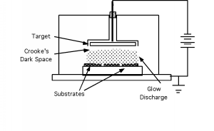
    Figure \(\PageIndex{1}\): Sputtering apparatus

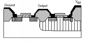
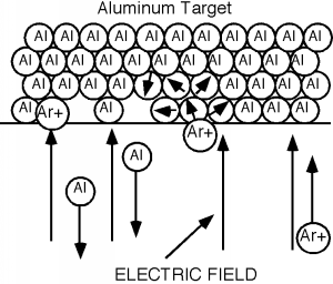
    The electric field accelerates the argon atoms which slam into the aluminum target. There is an exchange of momentum, and an aluminum atom is ejected from the target (Figure \(\PageIndex{2}\)) and heads to the silicon wafer, where it sticks, and builds up a metal film (Figure \(\PageIndex{3}\)).

    An aluminum target lies at the top of the image, and an electric field points upwards at it. The electric field propels argon ions into the target, displacing some aluminum atoms that move downwards, in the opposite direction of the argon.
    Figure \(\PageIndex{2}\): Sputtering mechanism
    The entire top of the wafer assembly from Figure 14 of the previous section is coated with a layer of metal.
    Figure \(\PageIndex{3}\): Wafer Coated with Metal

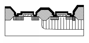
    If you look at Figure \(\PageIndex{3}\), you will note that we have seemingly done something pretty stupid. We have wired all of the elements of our CMOS inverter together! Ah, but all is not lost. We can do one more photolithographic step, and pattern and etch the aluminum, so we only have it where we need it. This is shown in Figure \(\PageIndex{4}\).

    The wafer from Figure 3 above has the portions of its metal coating that cover the underlying oxide layer removed.
    Figure \(\PageIndex{4}\): After interconnect patterning

    This page titled 9.5.8: Applying Metal/Sputtering is shared under a CC BY-NC-SA 1.0 license and was authored, remixed, and/or curated by Bill Wilson via source content that was edited to the style and standards of the LibreTexts platform; a detailed edit history is available upon request.