
1. Open-Circuit Properties
- Page ID
- 5966
The p-n junction has two important open-circuit properties -- that is, properties that arise when there are no external connections to the device. These are the barrier potential and the space-charge region. These properties emerge from the interactions among free electrons and holes in the n- and p-type sections.
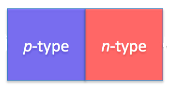
A p-n junction consists of one piece of p-type semiconductor adjacent to a piece of n-type semiconductor.
Barrier Potential
Recall that the p-type material has an excess of holes, while the n-type material has an excess of electrons; when moving from the p-type material to the n-type material, the concentration of holes (or free electrons) will change. If you were to physically move a positive charge (a hole) from a point within the region with a high concentration of holes (point x1, below) to a point within the region with a high concentration of electrons (point x2), energy would be released, since the positively-charged hole is attracted to the negatively-charged electrons. Recall that voltage is defined as the work required to move a positive charge across a distance; therefore, we see that a voltage will be established across any distance where there is a concentration gradient of charges.
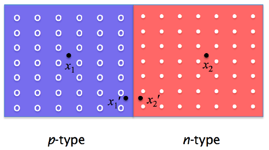
Moving a charge from x1 to x2 involves a release of energy - therefore, there is a voltage difference.
The same voltage exists between x1' and x2' (explained below); therefore the voltage difference is across the intersection point.
According to Bobrow1, the formula for the voltage difference across a hole gradient is the following:
v0 = VT ln(p1/p2),
where VT = T / 11,586 ( = 0.0259 at room temperature of T = 300 K), p1 is the hole concentration at x1, and p2 is the hole concentration at point x2. Note that this formula depends only on the difference in hole concentration between the two points and not the distance separating them; therefore, if we assume the hole and electron concentrations are constant throughout the p-type and n-type sections, respectively, we can see that the exact same voltage difference would be found between points x1' and x2' as between x1 and x2. Furthermore, we could move x1' and x2' arbitrarily close to the junction line and still find the same voltage. Therefore, the voltages within the p- and n-type materials must be constant, and the difference must occur only at the junction line.
Now let's simplify the equation. The concentration of holes in the p-type section (p1) is approximately equal to the concentration of acceptor atoms, NA. The mass-action law says that, at all times, the product of the hole concentration (p) and free electron concentration (n) is equal to the square of the intrinsic concentration (ni) of the semiconductor:
np = ni2.
Therefore, the hole concentration in the n-type section is p = ni2/n. Since the free electron concentration is approximately equal to the donor atom concentration ND, we have p = ni2/ND, an expression which contains all easily measureable quantities. Plugging these expressions for p1 and p2 into Bobrow's equation, we find:
v0 = VT ln (NAND/ni2)
This is the formula for the barrier potential of a p-n junction. Note that this is the voltage difference in the direction from n-type towards p-type. In reality, the hole and electron concentrations will not be constant throughout the material and will decrease as you move towards the junction line. However, the approximations made here still produce a formula for the barrier voltage that is reasonably accurate with empirical results.
Space-Charge Region
Consider again the locations and concentrations of charge carriers within the p- and n-type material. The p-type material will have a high concentration of holes and low concentration of free electrons, and vice versa for the n-type material. But any time particles are contained in a crowded environment, they will naturally diffuse out of that environment. Therefore, this steep concentration gradient will result in the diffusion of majority carriers across the junction line -- holes will diffuse into the n-type side and free electrons will diffuse into the p-type side. The free electrons will recombine with the holes, leaving this area depleted of charge carriers. This area is called the space-charge region, or the depletion region.
Recall that the p-type material is doped with Group 3 atoms, which have an ionic core charge of +3 and are surrounded by three valence electrons (charge -3). When placed in the semiconductor lattice, they create an excess hole. If this hole is filled by an electron that diffuses across the junction line, then the acceptor will still have an ionic core charge of +3 but will now be surrounded by 4 valence electrons. Therefore, the acceptor atoms in the space-charge region will have a charge of -1. The opposite is true for the Group 5 donor atoms in the n-type material, which normally have an ionic core charge of +5 and are surrounded by five valence electrons. When put into the semiconductor lattice, however, the fifth electron cannot covalent bond and is therefore a free electron. If the free electron diffuses across the junction-line, then the +5 ionic core will only be surrounded by 4 valence electrons; it will then carry a charge of +1. Therefore, the space-charge region consists of a region of negative ions in the p-type material, and a region of positive ions in the n-type material (see figure below). This juxtaposition of positive and negative ions creates an electric field within the material, pointed from n-type to p-type.
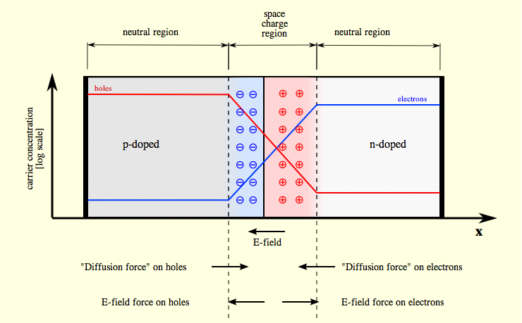
The diffusion of electrons and holes across the junction line creates uncovered ions in the space-charge region. These ions
create an electric field within the material, which further affect the carriers (explained below). Image courtesy of Wikimedia Commons.
The electric field resulting from the uncovered ions in the space-charge region will tend to push free electrons back into the n-type material and holes back into the p-type material. This force, which opposes diffusion, is called "drift". Drift gets stronger as diffusion increases, so it will prevent all the majority carriers from diffusing across the junction line. The charges will eventually orient themselves in such a manner that the diffusive and drift forces are exactly opposite.
References
- "Chapter 6: Diodes." Fundamentals of Electrical Engineering. 2nd ed. New York, New York: Oxford UP, 1996. 352-54. Print.