
3: Reverse Bias
- Page ID
- 5968
When an external voltage is applied across a p-n junction diode, we say there is a bias on the diode. When the voltage on the n side is higher than the voltage on the p side, we say the diode is under reverse bias. One application of reverse-biased diodes is Zener diodes.
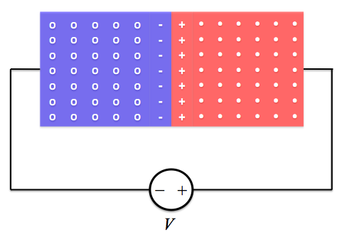
p-n junction diode under reverse bias. The p side is blue; the n side is red.
Reverse bias
Under reverse bias, the n side is held at a higher voltage than the p side. If the applied voltage is V, then the total potential difference across the diode becomes Vreverse bias = v0 + V (where v0 is the barrier potential).
Therefore, in the figure above, free electrons on the n side (negative charge) will experience a drift force to the right (towards the positive cathode). As before, they also experience a diffusive force to the left. The electrons that are close to the space charge region will experience the greatest diffusive force, since they are closest to the place of diffusion; these electrons will diffuse into the space charge region. The electrons further away from the space charge region will experience a greater drift force than a diffusive force and will therefore drift to the right. At the same time, the holes on the p side will experience a drift force to the left and a diffusive force to the right. The opposite will then happen from the electrons on the n side: the holes closest to the center will diffuse into the space charge region where they will recombine with the diffusing electrons. The holes furthest from the space charge region will drift towards the anode. Increased recombination due to diffusion, and carrier migration away from the space charge region due to drift, will combine to produce the net effect of a wider space charge region.
Now consider minority carriers in their respective material. For a free electron in the p-type material, the drift force is to the right. The diffusive force is negligible because the density of minority carriers is low (by definition!). As this electron moves to the right, it is likely to recombine with a hole. However, some electrons will make it across the p side without recombining and enter the space charge region, where they will be pushed across by the electric field. [The opposite will happen for holes on the n side] The result is a small current directed to the left, called the saturation current. For p-n junction diodes made from silicon, the saturation current is on the order of a nanoampere, 10-9 A.
As long as the diode is reverse biased, the saturation current is generally independent of the magnitude of V; however, if V becomes too large, the diode will break down and allow virtually any amount of current through. This characteristic is called breakdown, and it will typically destroy p-n junction diodes. p-n junction diodes that are designed to be used in breakdown are called Zener diodes.
Zener diodes
Zener diodes are simply reverse-biased diodes that can withstand operating in breakdown. As the reverse bias voltage increases, Zener diodes continue to conduct a constant amount of current (the saturation current), until a certain voltage is reached. At this voltage, known as the breakdown voltage, VZ, the diode will enter breakdown and allow nearly any amount of current through. Therefore, in breakdown, the magnitude of the current is determined by the other elements of the circuit (effective resistence, current sources, etc.). Breakdown voltages can range from 1 to 100 V.
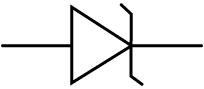
Circuit symbol for a Zener diode
Breakdown in Zener diodes is caused by two different, yet similar, means: the avalanche effect and the Zener effect. The avalanche effect occurs when the potential difference across the p-n junction becomes so great that free electrons crossing the junction gain enough energy to knock other covalently-bonded electrons out of their bonds by colliding with them. This collision creates a new electron-hole pair. The process then repeats, causing a chain reaction; almost instantly, a huge "avalanche" of charge carriers can be generated. This flood of new charge carriers represents a very sudden increase in current through the diode.
The Zener effect occurs when the electric field created by the space charge region becomes so strong that it can rip covalently-bonded electrons from their bonds. This also creates a new electron-hole pair, which will be quickly separated by the strong electric field. When the electric field becomes strong enough to separate many electrons and holes at a time, a large surge in current will result.
Zener diodes have useful applications in electronics. Because they permit large amounts of current, they can dissipate large amounts of power (P=IV). Zener diodes are also used in voltage regulators, devices that take a varying voltage input and output a constant voltage. The simplest voltage regulator can be created by placing a Zener diode in series with a resistor.
References
- "Chapter 6: Diodes." Fundamentals of Electrical Engineering. 2nd ed. New York, New York: Oxford UP, 1996. 361-62, 393-394. Print.
- "Avalanche Breakdown." Wikipedia. Wikimedia Foundation, 07 Mar. 2012. Web. 19 July 2012. <http://en.Wikipedia.org/wiki/Avalanche_breakdown>.
- "Voltage Regulator." Wikipedia. Wikimedia Foundation, 15 July 2012. Web. 19 July 2012. <http://en.Wikipedia.org/wiki/Voltage_regulator>.