
1.3: Bode Plots
- Page ID
- 3546

The Bode plot is a graphical response prediction technique that is useful for both circuit design and analysis. It is named after Hendrik Wade Bode, an American engineer known for his work in control systems theory and telecommunications. A Bode plot is, in actuality, a pair of plots: One graphs the gain of a system versus frequency, while the other details the circuit phase versus frequency. Both of these items are very important in the design of well-behaved, optimal operational amplifier circuits.
Generally, Bode plots are drawn with logarithmic frequency axes, a decibel gain axis, and a phase axis in degrees. First, let’s take a look at the gain plot. A typical gain plot is shown Figure \(\PageIndex{1}\).
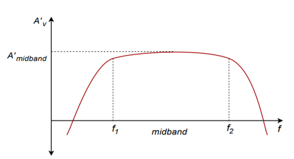
Figure \(\PageIndex{1}\): Gain plot.
Note how the plot is relatively flat in the middle, or midband, region. The gain value in this region is known as the midband gain. At either extreme of the midband region, the gain begins to decrease. The gain plot shows two important frequencies, \(f_1\) and \(f_2\). \(f_1\) is the lower break frequency while \(f_2\) is the upper break frequency. The gain at the break frequencies is 3 dB less than the midband gain. These frequencies are also known as the half-power points, or corner frequencies. Normally, amplifiers are only used for signals between \(f_1\) and \(f_2\). The exact shape of the rolloff regions will depend on the design of the circuit. It is possible to design amplifiers with no lower break frequency (i.e., a DC amplifier), however, all amplifiers will exhibit an upper break. The break points are caused by the presence of circuit reactances, typically coupling and stray capacitances. The gain plot is a summation of the midband response with the upper and lower frequency limiting networks. Let’s take a look at the lower break, \(f_1\).
1.3.1: Lead Network Gain Response
Reduction in low frequency gain is caused by lead networks. A generic lead network is shown in Figure \(\PageIndex{2}\). It gets its name from the fact that the output voltage developed across \(R\) leads the input. At very high frequencies the circuit will be essentially resistive. Conceptually, think of this as a simple voltage divider. The divider ratio depends on the reactance of \(C\). As the input frequency drops, \(X_c\) increases. This makes \(V_{out}\) decrease. At very high frequencies, where \(X_c \ll R\), \(V_{out}\) is approximately equal to \(V_{in}\). This can be seen graphically in Figure \(\PageIndex{3}\). The break frequency (i.e., the frequency at which the signal has decreased by 3 dB) is found via the standard equation
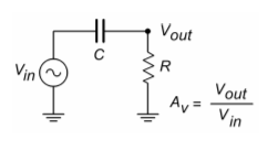
Figure \(\PageIndex{2}\): Lead network.
\[ f_c = \frac{1}{2 \pi RC} \nonumber \]
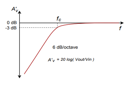
Figure \(\PageIndex{3}\): Lead gain plot (exact).
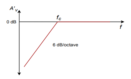
Figure \(\PageIndex{4}\): Lead gain plot (approximate).
The response below \(f_c\) will be a straight line if a decibel gain axis and a logarithmic frequency axis are used. This makes for very quick and convenient sketching of circuit response. The slope of this line is 6 dB per octave (an octave is a doubling or halving of frequency, e.g., 800 Hz is 3 octaves above 100 Hz).1 This range covers a factor of two in frequency. This slope may also be expressed as 20 dB per decade, where a decade is a factor of 10 in frequency. With reasonable accuracy, this curve may be approximated as two line segments, called asymptotes, as shown in Figure \(\PageIndex{4}\). The shape of this curve is the same for any lead network. Because of this, it is very easy to find the approximate gain at any given frequency as long as \(f_c\) is known. It is not necessary to go through reactance and phasor calculations. To create a general response equation, start with the voltage divider rule to find the gain:
\[\frac{V_{out}}{V_{in}} = \frac{R}{R-j\ X_c} \\ \frac{V_{out}}{V_{in}} = \frac{R \angle 0}{\sqrt{R^2+X_c^2}\angle −\arctan \frac{X_c}{R}} \nonumber \]
The magnitude of this is,
\[|A_v| = \frac{R}{\sqrt{R^2+X_c^{2}}} \\ |A_v| = \frac{1}{\sqrt{1+\frac{X_c^{2}}{R^2}}} \label{1.5} \]
Recalling that,
\[ f_c = \frac{1}{2 \pi R\ C} \nonumber \]
we may say,
\[ R = \frac{1}{2 \pi f_c\ C} \nonumber \]
For any frequency of interest, \(f\),
\[ X_c = \frac{1}{2 \pi f_c\ C} \nonumber \]
Equating the two preceding equations yields,
\[ \frac{f_c}{f} = \frac{X_c}{R} \label{1.6} \]
Substituting Equation \ref{1.6} in Equation \ref{1.5} gives,
\[ A_v = \frac{1}{\sqrt{1+\frac{f_c^2}{f^2}}} \label{1.7} \]
To express \(A_v\) in dB, substitute Equation \ref{1.7} into Equation 1.2.2
\[ A_v^{'} = 20 \log_{10} \frac{1}{\sqrt{1+\frac{f_c^2}{f^2}}} \nonumber \]
After simplification, the final result is:
\[ A_v^{'} = -10 \log_{10} \left(1+\frac{f_c^2}{f^2}\right) \label{1.8} \]
Where
\(f_c\) is the critical frequency,
\(f\) is the frequency of interest,
\(A^{'}_v\) is the decibel gain at the frequency of interest.
Example \(\PageIndex{1}\)
An amplifier has a lower break frequency of 40 Hz. How much gain is lost at 10 Hz?
\[A_v^{'} = - 10 \log_{10} \left(1+\frac{f_c^2}{f^2}\right) \\ A_v^{'} = -10 \log_{10} \left(1+\frac{40^2}{10^2}\right) \\ A_v^{'} = -12.3\ dB \nonumber \]
In other words, the gain is 12.3 dB lower than it is in the midband. Note that 10 Hz is 2 octaves below the break frequency. Because the cutoff slope is 6 dB per octave, each octave loses 6 dB. Therefore, the approximate result is -12 dB, which double-checks the exact result. Without the lead network, the gain would stay at 0 dB all the way down to DC (0 Hz.)
1.3.2: Lead Network Phase Response
At very low frequencies, the circuit of Figure \(\PageIndex{2}\) is largely capacitive. Because of this, the output voltage developed across \(R\) leads by 90 degrees. At very high frequencies the circuit will be largely resistive. At this point \(V_{out}\) will be in phase with \(V_{in}\). At the critical frequency, \(V_{out}\) will lead by 45 degrees. A general phase graph is shown in Figure \(\PageIndex{5}\). As with the gain plot, the phase plot shape is the same for any lead network. The general phase Equation may be obtained from the voltage divider:
\[ \frac{V_{out}}{V_{in}} = \frac{R}{R-j\ X_c} \\ \frac{V_{out}}{V_{in}} = \frac{R\angle 0}{\sqrt{R^2 + X_c^2}\angle −\arctan \frac{X_c}{R}} \nonumber \]
The phase portion of this is,
\[ \theta = \arctan \frac{X_c}{R} \nonumber \]
By using Equation \ref{1.6}, this simplifies to,
\[ \theta = \arctan \frac{f_c}{f} \label{1.9} \]
Where
\(f_c\) is the critical frequency,
\(f\) is the frequency of interest,
\(\theta\) is the phase angle at the frequency of interest.
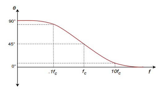
Figure \(\PageIndex{5}\): Lead phase (exact).
Often, an approximation such as Figure \(\PageIndex{6}\) used in place of \(\PageIndex{5}\). By using Equation \ref{1.9}, you can show that the approximation is off by no more than 6 degrees at the corners.
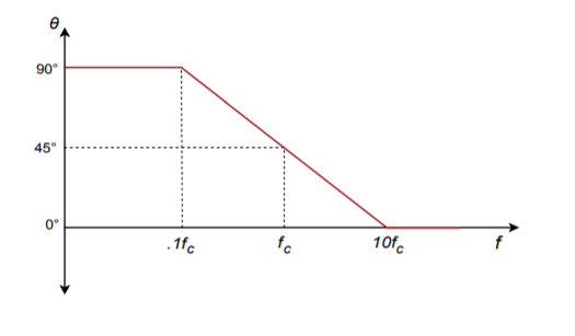
Figure \(\PageIndex{6}\): Lead phase (approximate).
Example \(\PageIndex{2}\)
A telephone amplifier has a lower break frequency of 120 Hz. What is the phase response one decade below and one decade above?
One decade below 120 Hz is 12 Hz, while one decade above is 1.2 kHz.
\[\theta = \arctan \frac{f_c}{f} \\ \theta = \arctan \frac{120\ Hz}{12\ Hz} \nonumber \]
\(\theta = 84.3\) degrees one decade below \(f_c\) (i.e, approaching 90 degrees)
\[ \theta = \arctan \frac{120}{1.2\ kHz} \nonumber \]
\(\theta = 5.71\) degrees one decade above \(f_c\) (i.e., approaching 0 degrees)
Remember, if an amplifier is direct-coupled, and has no lead networks, the phase will remain at 0 degrees right back to 0 Hz (DC).
1.3.3: Lag Network Response
Unlike its lead network counterpart, all amplifiers will contain lag networks. In essence, it’s little more than an inverted lead network. As you can see from Figure \(\PageIndex{7}\), it simply transposes the \(R\) and \(C\) locations. Because of this, the response tends to be inverted as well. In terms of gain, \(X_c\) is very large at low frequencies, and thus \(V_{out}\) equals \(V_{in}\). At high frequencies, \(X_c\) decreases, and \(V_{out}\) falls. The break point occurs when \(X_c\) equals \(R\). The general gain plot is shown in Figure \(\PageIndex{8}\). Like the lead network response, the slope of this curve is -6 dB per octave (or -20 dB per decade.) Note that the slope is negative instead of positive. A straight-line approximation is shown in Figure \(\PageIndex{9}\). We can derive a general gain Equation for this circuit in virtually the same manner as we did for the lead network. The derivation is left as an exercise.
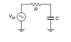
Figure \(\PageIndex{7}\): Lag network.
\[ A_v^{'} = -10 \log_{10} \left(1+\frac{f^2}{f_c^2} \right) \label{1.10} \]
Where
\(f_c\) is the critical frequency,
\(f\) is the frequency of interest,
\(A^{'}_v\) is the decibel gain at the frequency of interest.
Note that this Equation is almost the same as Equation \ref{1.8}. The only difference is that \(f\) and \(f_c\) have been transposed.
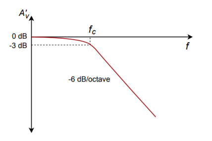
Figure \(\PageIndex{8}\): Lag gain (exact).
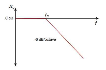
Figure \(\PageIndex{9}\): Lag gain (approximate).
In a similar vein, we may examine the phase response. At very low frequencies, the circuit is basically capacitive. Because the output is taken across \(C\), \(V_{out}\) will be in phase with \(V_{in}\). At very high frequencies, the circuit is essentially resistive. Consequently, the output voltage across \(C\) will lag by 90 degrees. At the break frequency the phase will be -45 degrees. A general phase plot is shown in Figure \(\PageIndex{10}\), with the approximate response detailed in Figure \(\PageIndex{11}\). As with the lead network,we may derive a phase equation. Again, the exact steps are very similar, and left as an exercise.
\[ \theta = -90 + \arctan \frac{f_c}{f} \label{1.11} \]
Where \(f_c\) is the critical frequency,
\(f\) is the frequency of interest,
\(\theta \) is the phase angle at the frequency of interest.
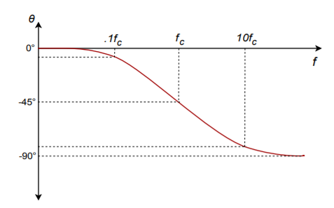
Figure \(\PageIndex{10}\): Lag phase (exact).
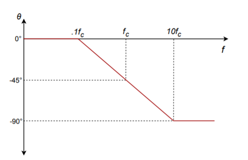
Figure \(\PageIndex{11}\): Lag phase (approximate).
Example \(\PageIndex{3}\)
A medical ultra sound transducer feeds a lag network with an upper break frequency of 150 kHz. What are the gain and phase values at 1.6 MHz? Because this represents a little more than a 1 decade increase, the approximate values are -20 dB and -90 degrees, from Figures \(\PageIndex{9}\) and \(\PageIndex{11}\), respectively. The exact values are:
\[A_v^{'} = -10 \log_{10} \left(1+\frac{f^2}{f_c^2}\right) \\ A_v^{'} = -10 \log_{10} \left(1+\frac{1.6\ MHz^2}{150\ MHz^2}\right) \\ A_v^{'} = -20.6\ dB \nonumber \]
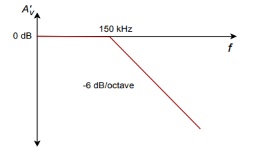
Figure \(\PageIndex{12}\): Bode plot for 150 kHz lag.
\[\theta = -90 + \arctan \frac{f_c}{f} \\ \theta = -90 + \arctan \frac{150\ kHz}{1.6\ MHz} \\ \theta = -84.6\ degrees \nonumber \]
The complete Bode plot for this network is shown in Figure \(\PageIndex{12}\). It is very useful to examine both plots simultaneously. In this manner you can find the exact phase change for a given gain quite easily. This information is very important when the application of negative feedback is considered (Chapter Three). For example, if you look carefully at the plots of Figure \(\PageIndex{12}\), you will note that at the critical frequency of 150 kHz, the total phase change is -45 degrees. Because this circuit involved the use of a single lag network, this is exactly what you would expect.
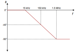
Figure \(\PageIndex{13}\): (continued) Bode plot for 150 kHz lag.
1.3.4: rise time versus Bandwidth
For pulse-type signals, the speed of an amplifier is often expressed in terms of its rise time. If a square pulse such as Figure \(\PageIndex{13a}\) is passed into a simple lag network, the capacitor charging effect will produce a rounded variation, as seen in Figure \(\PageIndex{13b}\). This effect places an upper limit on the duration of pulses that a given amplifier can handle without producing excessive distortion.
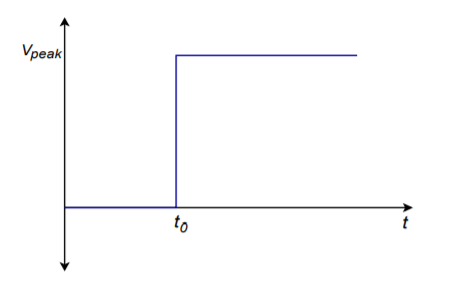
Figure \(\PageIndex{14a}\): Pulse rise time effect: Input to network.
By definition, rise time is the amount of time it takes for the signal to traverse from 10% to 90% of the peak value of the pulse. The shape of this pulse is defined by the standard capacitor charge Equation examined in earlier course work, and is valid for any system with a single clearly dominant lag network.
\[ V_{out} = V_{peak}\left(1-\epsilon^{\frac{-t}{RC}}\right) \label{1.12}\tag{1.12} \]
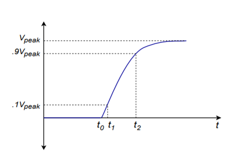
Figure \(\PageIndex{14b}\): Pulse rise time effect: Output of network.
In order to find the time internal from the initial starting point to the 10% point, set \(V_{out}\) to \(0.1\ V_{peak}\) in Equation \ref{1.12} and solve for \(t_1\).
\[ 0.1 V_{peak} = V_{peak}\left(1-\epsilon^{\frac{-t_1}{RC}}\right) \\ 0.1 V_{peak} = V_{peak} - V_{peak}\ \epsilon^{\frac{-t_1}{RC}} \\ 0.9 V_{peak} = V_{peak}\ \epsilon^{\frac{-t_1}{RC}} \\ 0.9 = \epsilon^{\frac{-t_1}{RC}} \\ \log\ 0.9 = \frac{-t_1}{RC} \\ t_1 = 0.105\ RC \label{1.13} \]
To find the interval up to the 90% point, follow the same technique using \(0.9\ V_{peak}\). Doing so yields
\[ t_2 = 2.303\ RC \label{1.14} \]
The rise time, \(T_r\), is the difference between \(t_1\) and \(t_2\)
\[T_r = t_1 - t_2 \\ T_r = 2.303\ RC - 0.105\ RC \\ T_r \approx 2.2\ RC \label{1.15} \]
Equation \ref{1.15} ties the rise time to the lag network’s \(R\) and \(C\) values. These same values also set the critical frequency \(f_2\). By combining Equation \ref{1.15} with basic critical frequency relationship, we can derive an Equation relating \(f_2\) to \(T_r\).
\[ f_2 = \frac{1}{2 \pi RC} \nonumber \]
Solving \ref{1.15} in terms of \(RC\), and substituting yields
\[ f_2 = \frac{2.2}{2 \pi T_r} \\ f_2 = \frac{0.35}{T_r} \label{1.16} \]
Where \(f_2\) is the upper critical frequency,
\(T_r\) is the rise time of the output pulse.
Example \(\PageIndex{4}\)
Determine the rise time for a lag network critical at 100 kHz.
\[ f_2 = \frac{0.35}{T_r} \\ T_r = \frac{0.35}{f_2} \\ T_r = \frac{0.35}{100\ kHz} \\ T_r = 3.5\ \mu s \nonumber \]
References
1The term octave is borrowed from the field of music. It gets its name from the fact that there are eight notes in the standard western scale: do-re-me-fa-so-la-ti-do.