
7.7: Extended Topic
- Page ID
- 11229

7.7.1: A Precision Log Amp
The basic log amplifier discussed earlier suffers from two major problems: repeatability and temperature sensitivity. Let's take a closer look at Equation 7.6.5. First, if you work backward through the derivation, you will notice that the constant 0.0259 is actually \(K T/q\) using a temperature of 300 K. Thus, we may rewrite this Equation as,
\[ V_{out} =− \frac{K T}{q} ln \frac{V_{in}}{R_i I_s} \label{7.19} \]
Note that the output voltage is directly proportional to the circuit temperature, \(T\). Normally, this is not desired. The second item of interest is \(I_s\). This current can vary considerably between devices, and is also temperature sensitive, approximately doubling for each 10 C\(^{\circ}\) rise. For these reasons, commercial log amps such as those mentioned earlier, are preferred. This does not mean that it is impossible to create stable log amps from the basic op amp building blocks. To the contrary, a closer look at practical circuit solutions will point out why specialised log ICs are successful. We shall treat the two problems separately.
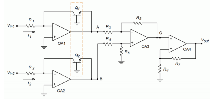
Figure \(\PageIndex{1}\): A high quality log amplifier.
One way of removing the effect of \(I_s\) from our log amp is to subtract away an equal effect. The circuit of Figure \(\PageIndex{1}\) does exactly this. This circuit utilizes two log amps. Although each is drawn with an input resistor and input voltage source, removal of \(R_1\) and \(R_2\) would allow current sensing inputs. Each log amp's transistor is part of a matched pair. These two transistors are fabricated on the same silicon wafer and exhibit nearly identical characteristics (in our case, the most notable being \(I_s\)).
Based on Equation \ref{7.19} we find
\[ V_A = \frac{−K T}{q} ln \frac{V_{in1}}{R_1 I_{s1}} \nonumber \]
\[ V_B = \frac{−K T}{q} ln \frac{V_{in2}}{R_2 I_{s2}} \nonumber \]
Where typically, \(R_1 = R_2\). These two signals are fed into a differential amplifier comprised of op amp 3, and resistors \(R_3\) through \(R_6\). It is normally set for a gain of unity. The output of the differential amplifier (point C) is
\[ V_C = V_B − V_A \nonumber \]
\[ V_C = \frac{−K T}{q} ln \frac{V_{in2}}{R_2 I_{s2}} – \left( − \frac{K T}{q} ln \frac{V_{in1}}{R_1 I_{s1}} \right) \nonumber \]
\[ V_C = \frac{K T}{q} \left( ln \frac{V_{in1}}{R_1 I_{s1}} − ln \frac{V_{in2}}{R_2 I_{s2}} \right) \label{7.20} \]
Using the basic identity that subtracting logs is the same as dividing their arguments, \ref{7.20} becomes
\[ V_C = \frac{K T}{q} ln \frac{\frac{V_{in1}}{R_1 I_{s1}}}{\frac{V_{in2}}{R_2 I_{s2}}} \label{7.21} \]
Because \(R_1\) is normally set equal to \(R_2\), and \(I_{s1}\) and \(I_{s2}\) are identical due to the fact that \(Q_1\) and \(Q_2\) are matched devices, \ref{7.21} simplifies to
\[ V_C = \frac{K T}{q} ln \frac{V_{in1}}{V_{in2}} \label{7.22} \]
As you can see, the effect of \(I_s\) has been removed. \(V_C\) is a function of the ratio of the two inputs. Therefore, this circuit is called a log ratio amplifier. The only remaining effect is that of temperature variation. Op amp 4 is used to compensate for this. This stage is little more than a standard SP noninverting amplifier. What makes it unique is that \(R_8\) is a temperature-sensitive resistor. This component has a positive temperature coefficient of resistance, meaning that as temperature rises, so does its resistance. Because the gain of this stage is \(1 + (R_7/R_8)\), a temperature rise causes a decrease in gain. Combining this with \ref{7.22} produces
\[ V_{out} = \left( 1+ \frac{R_7}{R_8} \right) \frac{K T}{q} ln \frac{V_{in1}}{V_{in2}} \label{7.23} \]
If the temperature coefficient of \(R_8\) is chosen correctly, the first two temperature dependent terms of \ref{7.23} will cancel, leaving a temperature stable circuit. This coefficient is approximately 1/300 K, or 0.33% per C\(^{\circ}\), in the vicinity of room temperature.
Our log ratio circuit is still not complete. Although the major stability problems have been eliminated, other problems do exist. It is important to note that the transistor used in the feedback loop loads the op amp, just as the ordinary feedback resistor \(R_f\) would. The difference lies in the fact that the effective resistance, which the op amp sees is, the dynamic base-emitter resistance, \(r^{'}_e\). This resistance varies with the current passing through the transistor and has been found to equal 26m \(V/I_E\) at room temperature. For higher input currents this resistance can be very small and might lead to an overload condition. A current of 1 mA, for example, would produce an effective load of only 26 \(\Omega\). This problem can be alleviated by inserting a large value resistance in the feedback loop. This resistor, labeled \(R_E\), is shown in Figure \(\PageIndex{2}\). An appropriate value for \(R_E\) may be found by realizing that at saturation, virtually all of the output potential will be dropped across \(R_E\), save \(V_{BE}\). The current through \(R_E\) is the maximum expected input current plus load current. Using Ohm's Law,
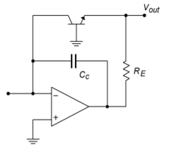
Figure \(\PageIndex{2}\): Compensation components.
\[ R_E = \frac{V_{sat} − V_{BE}}{I_{max}} \label{7.24} \]
Figure \(\PageIndex{2}\) also shows a compensation capacitor, \(C_c\). This capacitor is used to roll off high frequency gain in order to suppress possible high frequency oscillations. An optimum value for \(C_c\) is not easy to determine, as the feedback element's resistance changes with the input level. It may be found empirically in the laboratory. A typical value would be in the vicinity of 100 pF.1
One possible application for the log ratio circuit is found in Figure \(\PageIndex{3}\). This system is used to measure the light transmission of a given material. Because variations in the light source will affect a direct measurement, the measurement is instead made relative to a known material. In this example, light is passed through a known medium (such as a vacuum) while it is simultaneously passed through the medium under test. On the far side of both materials are light-sensitive devices such as photodioides, phototransistors, or photomultiplier tubes. These devices will produce a current proportional to the amount of light striking them. In this system, these currents are fed into the log ratio circuit, which will then produce an output voltage proportional to the light transmission abilities of the new material. This setup eliminates the problem of light source fluctuation, because each input will see an equal percentage change in light intensity. Effectively, this is a common-mode signal that is suppressed by the differential amplifier section. This system also eliminates the difficulty of generating calibrated light intensity readings for comparisons. By its very nature, this system performs relative readings.
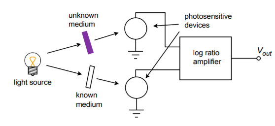
Figure \(\PageIndex{3}\): Light transmission measurement.
References
1A detailed derivation for Cc may be found in Daniel H. Sheingold, ed., 2d ed. Nonlinear Circuits Handbook, (Norwood, Mass.: Analog Devices, 1976) pp 174–178.