
6.3: Crystallography Revisited
- Page ID
- 18974

\( \newcommand{\vecs}[1]{\overset { \scriptstyle \rightharpoonup} {\mathbf{#1}} } \)
\( \newcommand{\vecd}[1]{\overset{-\!-\!\rightharpoonup}{\vphantom{a}\smash {#1}}} \)
\( \newcommand{\dsum}{\displaystyle\sum\limits} \)
\( \newcommand{\dint}{\displaystyle\int\limits} \)
\( \newcommand{\dlim}{\displaystyle\lim\limits} \)
\( \newcommand{\id}{\mathrm{id}}\) \( \newcommand{\Span}{\mathrm{span}}\)
( \newcommand{\kernel}{\mathrm{null}\,}\) \( \newcommand{\range}{\mathrm{range}\,}\)
\( \newcommand{\RealPart}{\mathrm{Re}}\) \( \newcommand{\ImaginaryPart}{\mathrm{Im}}\)
\( \newcommand{\Argument}{\mathrm{Arg}}\) \( \newcommand{\norm}[1]{\| #1 \|}\)
\( \newcommand{\inner}[2]{\langle #1, #2 \rangle}\)
\( \newcommand{\Span}{\mathrm{span}}\)
\( \newcommand{\id}{\mathrm{id}}\)
\( \newcommand{\Span}{\mathrm{span}}\)
\( \newcommand{\kernel}{\mathrm{null}\,}\)
\( \newcommand{\range}{\mathrm{range}\,}\)
\( \newcommand{\RealPart}{\mathrm{Re}}\)
\( \newcommand{\ImaginaryPart}{\mathrm{Im}}\)
\( \newcommand{\Argument}{\mathrm{Arg}}\)
\( \newcommand{\norm}[1]{\| #1 \|}\)
\( \newcommand{\inner}[2]{\langle #1, #2 \rangle}\)
\( \newcommand{\Span}{\mathrm{span}}\) \( \newcommand{\AA}{\unicode[.8,0]{x212B}}\)
\( \newcommand{\vectorA}[1]{\vec{#1}} % arrow\)
\( \newcommand{\vectorAt}[1]{\vec{\text{#1}}} % arrow\)
\( \newcommand{\vectorB}[1]{\overset { \scriptstyle \rightharpoonup} {\mathbf{#1}} } \)
\( \newcommand{\vectorC}[1]{\textbf{#1}} \)
\( \newcommand{\vectorD}[1]{\overrightarrow{#1}} \)
\( \newcommand{\vectorDt}[1]{\overrightarrow{\text{#1}}} \)
\( \newcommand{\vectE}[1]{\overset{-\!-\!\rightharpoonup}{\vphantom{a}\smash{\mathbf {#1}}}} \)
\( \newcommand{\vecs}[1]{\overset { \scriptstyle \rightharpoonup} {\mathbf{#1}} } \)
\(\newcommand{\longvect}{\overrightarrow}\)
\( \newcommand{\vecd}[1]{\overset{-\!-\!\rightharpoonup}{\vphantom{a}\smash {#1}}} \)
\(\newcommand{\avec}{\mathbf a}\) \(\newcommand{\bvec}{\mathbf b}\) \(\newcommand{\cvec}{\mathbf c}\) \(\newcommand{\dvec}{\mathbf d}\) \(\newcommand{\dtil}{\widetilde{\mathbf d}}\) \(\newcommand{\evec}{\mathbf e}\) \(\newcommand{\fvec}{\mathbf f}\) \(\newcommand{\nvec}{\mathbf n}\) \(\newcommand{\pvec}{\mathbf p}\) \(\newcommand{\qvec}{\mathbf q}\) \(\newcommand{\svec}{\mathbf s}\) \(\newcommand{\tvec}{\mathbf t}\) \(\newcommand{\uvec}{\mathbf u}\) \(\newcommand{\vvec}{\mathbf v}\) \(\newcommand{\wvec}{\mathbf w}\) \(\newcommand{\xvec}{\mathbf x}\) \(\newcommand{\yvec}{\mathbf y}\) \(\newcommand{\zvec}{\mathbf z}\) \(\newcommand{\rvec}{\mathbf r}\) \(\newcommand{\mvec}{\mathbf m}\) \(\newcommand{\zerovec}{\mathbf 0}\) \(\newcommand{\onevec}{\mathbf 1}\) \(\newcommand{\real}{\mathbb R}\) \(\newcommand{\twovec}[2]{\left[\begin{array}{r}#1 \\ #2 \end{array}\right]}\) \(\newcommand{\ctwovec}[2]{\left[\begin{array}{c}#1 \\ #2 \end{array}\right]}\) \(\newcommand{\threevec}[3]{\left[\begin{array}{r}#1 \\ #2 \\ #3 \end{array}\right]}\) \(\newcommand{\cthreevec}[3]{\left[\begin{array}{c}#1 \\ #2 \\ #3 \end{array}\right]}\) \(\newcommand{\fourvec}[4]{\left[\begin{array}{r}#1 \\ #2 \\ #3 \\ #4 \end{array}\right]}\) \(\newcommand{\cfourvec}[4]{\left[\begin{array}{c}#1 \\ #2 \\ #3 \\ #4 \end{array}\right]}\) \(\newcommand{\fivevec}[5]{\left[\begin{array}{r}#1 \\ #2 \\ #3 \\ #4 \\ #5 \\ \end{array}\right]}\) \(\newcommand{\cfivevec}[5]{\left[\begin{array}{c}#1 \\ #2 \\ #3 \\ #4 \\ #5 \\ \end{array}\right]}\) \(\newcommand{\mattwo}[4]{\left[\begin{array}{rr}#1 \amp #2 \\ #3 \amp #4 \\ \end{array}\right]}\) \(\newcommand{\laspan}[1]{\text{Span}\{#1\}}\) \(\newcommand{\bcal}{\cal B}\) \(\newcommand{\ccal}{\cal C}\) \(\newcommand{\scal}{\cal S}\) \(\newcommand{\wcal}{\cal W}\) \(\newcommand{\ecal}{\cal E}\) \(\newcommand{\coords}[2]{\left\{#1\right\}_{#2}}\) \(\newcommand{\gray}[1]{\color{gray}{#1}}\) \(\newcommand{\lgray}[1]{\color{lightgray}{#1}}\) \(\newcommand{\rank}{\operatorname{rank}}\) \(\newcommand{\row}{\text{Row}}\) \(\newcommand{\col}{\text{Col}}\) \(\renewcommand{\row}{\text{Row}}\) \(\newcommand{\nul}{\text{Nul}}\) \(\newcommand{\var}{\text{Var}}\) \(\newcommand{\corr}{\text{corr}}\) \(\newcommand{\len}[1]{\left|#1\right|}\) \(\newcommand{\bbar}{\overline{\bvec}}\) \(\newcommand{\bhat}{\widehat{\bvec}}\) \(\newcommand{\bperp}{\bvec^\perp}\) \(\newcommand{\xhat}{\widehat{\xvec}}\) \(\newcommand{\vhat}{\widehat{\vvec}}\) \(\newcommand{\uhat}{\widehat{\uvec}}\) \(\newcommand{\what}{\widehat{\wvec}}\) \(\newcommand{\Sighat}{\widehat{\Sigma}}\) \(\newcommand{\lt}{<}\) \(\newcommand{\gt}{>}\) \(\newcommand{\amp}{&}\) \(\definecolor{fillinmathshade}{gray}{0.9}\)Real Space and Reciprocal Space
Physicists and chemists are often interested in where electrons or nucleons of atoms are likely to be found with respect to position in real space. Ideas of a lattice, basis, and crystal structure were discussed in Sec. 2.3.2. To review, a lattice describes the arrangements of points. The basis describes how atoms are arranged at each lattice point. The lattice and basis together form the crystal structure. A 3D lattice is described by three lattice vectors \(\overrightarrow{a_1}\), \(\overrightarrow{a_2}\), and \(\overrightarrow{a_3}\). If they are chosen as short as possible, they are called primitive lattice vectors. The magnitude of a primitive lattice vector may be around 0.1 nm. The primitive lattice vectors define a cell called a primitive cell. Since a lattice is periodic, if we know how to describe one primitive cell, we can describe the entire lattice.
For each lattice, there is a corresponding reciprocal lattice defined by a set of vectors. Both contain the same information in different forms. For a 3D lattice with primitive vectors \(\overrightarrow{a_1}\), \(\overrightarrow{a_2}\), and \(\overrightarrow{a_3}\), the vectors of the reciprocal lattice are labeled by the vectors \(\overrightarrow{b_1}\), \(\overrightarrow{b_2}\), and \(\overrightarrow{b_3}\).
\[\overrightarrow{b_1} = \frac{2 \pi \overrightarrow{a_2} \times \overrightarrow{a_3}}{\overrightarrow{a_1} \cdot \overrightarrow{a_2} \times \overrightarrow{a_3}} \nonumber \]
\[\overrightarrow{b_2} = \frac{2 \pi \overrightarrow{a_3} \times \overrightarrow{a_1}}{\overrightarrow{a_1} \cdot \overrightarrow{a_2} \times \overrightarrow{a_3}} \nonumber \]
\[\overrightarrow{b_3} = \frac{2 \pi \overrightarrow{a_1} \times \overrightarrow{a_2}}{\overrightarrow{a_1} \cdot \overrightarrow{a_2} \times \overrightarrow{a_3}} \nonumber \]
Notice that \(\overrightarrow{b_1}\) is perpendicular to \(\overrightarrow{a_2}\) and \(\overrightarrow{a_3}\). Also, \(\overrightarrow{b_1}\) is parallel to \(\overrightarrow{a_1}\). More specifically, \( |\overrightarrow{b_1}| \cdot |\overrightarrow{a_1}| = 2 \pi\). (Factors of \(2 \pi \) show up due to choice of units, \(\frac{cycles}{m}\) vs \(\frac{rad}{m}\).) Thus if vector \(\overrightarrow{a_1}\) is long, \(\overrightarrow{b_1}\) will be short. Just as we can get from one lattice point to another by traveling integer multiples of the \(\overrightarrow{a_\mathfrak{n}}\) lattice vectors, we can get from any one point to the next of the reciprocal lattice by traveling integer multiples of the \(\overrightarrow{b_\mathfrak{n}}\) lattice vector. Lattice vectors in real space have units of length, \(m\). Lattice vectors in reciprocal space have units \(m^{-1}\).
The reciprocal lattice gives information about the spatial frequency of atoms. If the planes of atoms in a crystal are closely spaced in one direction, \(|\overrightarrow{a_1}|\) is relatively small. The corresponding reciprocal vector \(|\overrightarrow{b_1}|\) is relatively large. The reciprocal lattice represents the spatial frequency of the atom in units \(m^{-1}\). If the planes of atoms in a crystal are far apart, \(|\overrightarrow{a_1}|\) is large and \(|\overrightarrow{b_1}|\) is small.
If a beam of light shines on a crystal where the wavelength of light is close to the crystal spacing, light will be diffracted, and the diffraction pattern is related to the reciprocal lattice. The Brillouin zone is a primitive cell for a reciprocal lattice. The volume of a unit cell in reciprocal space over a unit cell in real space is given by
\[\frac{\text{vol. Brillouin zone}}{\text{vol. primitive cell in real space}} = \frac{\overrightarrow{b_1} \cdot \overrightarrow{b_2} \times \overrightarrow{b_3}}{\overrightarrow{a_1} \cdot \overrightarrow{a_2} \times \overrightarrow{a_3}} =(2\pi)^3. \nonumber \]
As for the real space lattice, to understand the reciprocal space lattice, we need to only understand one cell because the reciprocal space lattice is periodic.
versus k Diagrams
The energy level diagrams, discussed in Section 6.2, plot allowed energies of electrons where the vertical axis represented energy. No variation is shown on the horizontal axis. The most useful energy level diagrams for semiconductors are zoomed in so that only the valence and conduction band are shown. In many cases, it is useful to plot energy level diagrams versus position in real space. For such a diagram the vertical axis represents energy, and the horizontal axis represents position. It is also useful to plot energy level diagrams versus position in reciprocal space.
Kinetic energy is given by
\[E_{kinetic} = \frac{1}{2}m|\overrightarrow{v}|^2 = \frac{1}{2m}|\overrightarrow{M}|^2 \nonumber \]
where \(\overrightarrow{v}\) represents velocity in \(\frac{m}{s}\) and \(m\) represents mass in kg. Momentum is given by \(\overrightarrow{M} = m\overrightarrow{v}\) in units \(\frac{kg \cdot m}{s} = \frac{J \cdot s}{m}\). Electrons in crystals at \(T > 0\) K vibrate, and certain vibrations are resonant in the crystal. The crystal momentum \(\overrightarrow{M}_{crystal}\) represents the internal momentum of due to vibrations. It can be expressed as
\[\overrightarrow{M}_{crystal} = \hbar\overrightarrow{k} \nonumber \]
and has units of momentum\(\frac{kg \cdot m}{s}\). The quantity \(\overrightarrow{k}\) is called the wave vector, and it has units \(m^{-1}\). It represents change in spatial frequency, a distance in reciprocal space. The constant
\[\hbar = \frac{h}{2\pi} \nonumber \]
is called h-bar and is the Planck constant divided by \(2\pi\). Kinetic energy can be written in terms of the wave vector.
\[E_{kinetic} = \frac{\hbar^2 |\overrightarrow{k}|^2}{2m} \label{6.3.8} \]
Equation \ref{6.3.8} describes how energy of an electron varies with wave vector \(|\overrightarrow{k}|\) which incorporates information about lattice vibrations. The energy is quadratic in wave vector, so plots of energy versus \(|\overrightarrow{k}|\) are parabolic. Equation \ref{6.3.8} is just a model, and it applies best near the top of the valence band and bottom of the conduction band.
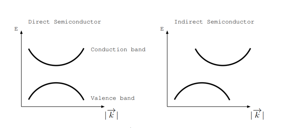
Energy versus \(|\overrightarrow{k}|\) diagrams plot allowed energy levels. Think of the \(|\overrightarrow{k}|\) axis as change in position in reciprocal space. If the top of the valence band and bottom of the conduction band occur at the same \(|\overrightarrow{k}|\) value in a semiconductor, we say that it is direct. If the top of valence band and bottom of conduction band occur at different \(|\overrightarrow{k}|\) values, we say that the semiconductor is indirect. The left part of Fig. \(\PageIndex{1}\) shows an energy versus \(|\overrightarrow{k}|\) diagram for a direct semiconductor, and the right part of Fig. \(\PageIndex{1}\) shows one for an indirect semiconductor. GaAs, InP, and ZnTe are direct semiconductors. Si, Ge, AlAs, and GaP are indirect semiconductors. Along different crystal axes, the band structure changes somewhat. The horizontal axis of an energy versus \(|\overrightarrow{k}|\) diagram may be specified along a particular axis in reciprocal space.
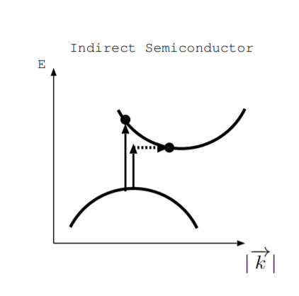
What happens when we shine light on a direct semiconductor? A photon of sufficient energy can excite an electron from the valence band to the conduction band to create an electron-hole pair. What happens in an indirect semiconductor? Figure \(\PageIndex{2}\) illustrates two possibilities. As illustrated by the longer arrow, an electron can be excited directly from the valence to conduction band. However, this requires a photon of more energy than the vertical distance between the top of the valence band and the bottom of the conduction band [25, p. 200]. Alternatively, as illustrated by the other two arrows, excitation from the top of the valence band to the bottom of the conduction band may involve a photon and a phonon. Both energy and momentum must be conserved, so a change in crystal momentum is needed to excite an electron in this case. Solar cells and photodetectors may be made from either direct or indirect semiconductors.