
4.4: Series-Parallel Circuit Analysis
- Page ID
- 25261

\( \newcommand{\vecs}[1]{\overset { \scriptstyle \rightharpoonup} {\mathbf{#1}} } \)
\( \newcommand{\vecd}[1]{\overset{-\!-\!\rightharpoonup}{\vphantom{a}\smash {#1}}} \)
\( \newcommand{\dsum}{\displaystyle\sum\limits} \)
\( \newcommand{\dint}{\displaystyle\int\limits} \)
\( \newcommand{\dlim}{\displaystyle\lim\limits} \)
\( \newcommand{\id}{\mathrm{id}}\) \( \newcommand{\Span}{\mathrm{span}}\)
( \newcommand{\kernel}{\mathrm{null}\,}\) \( \newcommand{\range}{\mathrm{range}\,}\)
\( \newcommand{\RealPart}{\mathrm{Re}}\) \( \newcommand{\ImaginaryPart}{\mathrm{Im}}\)
\( \newcommand{\Argument}{\mathrm{Arg}}\) \( \newcommand{\norm}[1]{\| #1 \|}\)
\( \newcommand{\inner}[2]{\langle #1, #2 \rangle}\)
\( \newcommand{\Span}{\mathrm{span}}\)
\( \newcommand{\id}{\mathrm{id}}\)
\( \newcommand{\Span}{\mathrm{span}}\)
\( \newcommand{\kernel}{\mathrm{null}\,}\)
\( \newcommand{\range}{\mathrm{range}\,}\)
\( \newcommand{\RealPart}{\mathrm{Re}}\)
\( \newcommand{\ImaginaryPart}{\mathrm{Im}}\)
\( \newcommand{\Argument}{\mathrm{Arg}}\)
\( \newcommand{\norm}[1]{\| #1 \|}\)
\( \newcommand{\inner}[2]{\langle #1, #2 \rangle}\)
\( \newcommand{\Span}{\mathrm{span}}\) \( \newcommand{\AA}{\unicode[.8,0]{x212B}}\)
\( \newcommand{\vectorA}[1]{\vec{#1}} % arrow\)
\( \newcommand{\vectorAt}[1]{\vec{\text{#1}}} % arrow\)
\( \newcommand{\vectorB}[1]{\overset { \scriptstyle \rightharpoonup} {\mathbf{#1}} } \)
\( \newcommand{\vectorC}[1]{\textbf{#1}} \)
\( \newcommand{\vectorD}[1]{\overrightarrow{#1}} \)
\( \newcommand{\vectorDt}[1]{\overrightarrow{\text{#1}}} \)
\( \newcommand{\vectE}[1]{\overset{-\!-\!\rightharpoonup}{\vphantom{a}\smash{\mathbf {#1}}}} \)
\( \newcommand{\vecs}[1]{\overset { \scriptstyle \rightharpoonup} {\mathbf{#1}} } \)
\(\newcommand{\longvect}{\overrightarrow}\)
\( \newcommand{\vecd}[1]{\overset{-\!-\!\rightharpoonup}{\vphantom{a}\smash {#1}}} \)
\(\newcommand{\avec}{\mathbf a}\) \(\newcommand{\bvec}{\mathbf b}\) \(\newcommand{\cvec}{\mathbf c}\) \(\newcommand{\dvec}{\mathbf d}\) \(\newcommand{\dtil}{\widetilde{\mathbf d}}\) \(\newcommand{\evec}{\mathbf e}\) \(\newcommand{\fvec}{\mathbf f}\) \(\newcommand{\nvec}{\mathbf n}\) \(\newcommand{\pvec}{\mathbf p}\) \(\newcommand{\qvec}{\mathbf q}\) \(\newcommand{\svec}{\mathbf s}\) \(\newcommand{\tvec}{\mathbf t}\) \(\newcommand{\uvec}{\mathbf u}\) \(\newcommand{\vvec}{\mathbf v}\) \(\newcommand{\wvec}{\mathbf w}\) \(\newcommand{\xvec}{\mathbf x}\) \(\newcommand{\yvec}{\mathbf y}\) \(\newcommand{\zvec}{\mathbf z}\) \(\newcommand{\rvec}{\mathbf r}\) \(\newcommand{\mvec}{\mathbf m}\) \(\newcommand{\zerovec}{\mathbf 0}\) \(\newcommand{\onevec}{\mathbf 1}\) \(\newcommand{\real}{\mathbb R}\) \(\newcommand{\twovec}[2]{\left[\begin{array}{r}#1 \\ #2 \end{array}\right]}\) \(\newcommand{\ctwovec}[2]{\left[\begin{array}{c}#1 \\ #2 \end{array}\right]}\) \(\newcommand{\threevec}[3]{\left[\begin{array}{r}#1 \\ #2 \\ #3 \end{array}\right]}\) \(\newcommand{\cthreevec}[3]{\left[\begin{array}{c}#1 \\ #2 \\ #3 \end{array}\right]}\) \(\newcommand{\fourvec}[4]{\left[\begin{array}{r}#1 \\ #2 \\ #3 \\ #4 \end{array}\right]}\) \(\newcommand{\cfourvec}[4]{\left[\begin{array}{c}#1 \\ #2 \\ #3 \\ #4 \end{array}\right]}\) \(\newcommand{\fivevec}[5]{\left[\begin{array}{r}#1 \\ #2 \\ #3 \\ #4 \\ #5 \\ \end{array}\right]}\) \(\newcommand{\cfivevec}[5]{\left[\begin{array}{c}#1 \\ #2 \\ #3 \\ #4 \\ #5 \\ \end{array}\right]}\) \(\newcommand{\mattwo}[4]{\left[\begin{array}{rr}#1 \amp #2 \\ #3 \amp #4 \\ \end{array}\right]}\) \(\newcommand{\laspan}[1]{\text{Span}\{#1\}}\) \(\newcommand{\bcal}{\cal B}\) \(\newcommand{\ccal}{\cal C}\) \(\newcommand{\scal}{\cal S}\) \(\newcommand{\wcal}{\cal W}\) \(\newcommand{\ecal}{\cal E}\) \(\newcommand{\coords}[2]{\left\{#1\right\}_{#2}}\) \(\newcommand{\gray}[1]{\color{gray}{#1}}\) \(\newcommand{\lgray}[1]{\color{lightgray}{#1}}\) \(\newcommand{\rank}{\operatorname{rank}}\) \(\newcommand{\row}{\text{Row}}\) \(\newcommand{\col}{\text{Col}}\) \(\renewcommand{\row}{\text{Row}}\) \(\newcommand{\nul}{\text{Nul}}\) \(\newcommand{\var}{\text{Var}}\) \(\newcommand{\corr}{\text{corr}}\) \(\newcommand{\len}[1]{\left|#1\right|}\) \(\newcommand{\bbar}{\overline{\bvec}}\) \(\newcommand{\bhat}{\widehat{\bvec}}\) \(\newcommand{\bperp}{\bvec^\perp}\) \(\newcommand{\xhat}{\widehat{\xvec}}\) \(\newcommand{\vhat}{\widehat{\vvec}}\) \(\newcommand{\uhat}{\widehat{\uvec}}\) \(\newcommand{\what}{\widehat{\wvec}}\) \(\newcommand{\Sighat}{\widehat{\Sigma}}\) \(\newcommand{\lt}{<}\) \(\newcommand{\gt}{>}\) \(\newcommand{\amp}{&}\) \(\definecolor{fillinmathshade}{gray}{0.9}\)Given the infinite variety of series-parallel configurations, there are myriad ways of solving any given circuit for a particular current or voltage. Many solution paths exist. This is good, because while you might not see a particular path, there are others that will also provide correct results. The only issue is which path is most efficient or convenient for you. Suppose we are trying to find \(v_b\) in the circuit of Figure \(\PageIndex{1}\). How might we approach this problem?
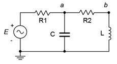
One path would be to find the total impedance seen by the voltage source, \(Z_{total}\). Dividing the source voltage by this impedance gives us the source current. We could then perform a current divider between the capacitor and inductor-resistor branches to find the inductor current. Once that current is found, it can be multiplied by the inductive reactance to find \(v_b\). Alternately, having found the total impedance, we could compute the voltage divider between the three components on the right and \(R_1\) to find \(v_a\). Knowing \(v_a\), a second voltage divider between \(X_L\) and \(R_2\) gives us \(v_b\). A third possibility would be to find the source current and use that to find \(v_a\), perhaps by finding the drop across \(R_1\) and subtracting that from the source, \(E\). Once \(v_a\) is found, a voltage divider can be used to find \(v_b\). Undoubtedly there are other solution paths that will work here. Some are more “computationally expensive” than others, but as long as you can identify one of them, the answers are within reach. Remember, the larger the circuit becomes, the greater the number of possible solution paths. Don't fall into the trap of relying on the same “trick” for every circuit, though. It is useful to solve these circuits using a variety of techniques as a means of cross-checking the results and sharpening your skill set.
Example \(\PageIndex{1}\)
Determine \(v_b\) for the circuit of Figure \(\PageIndex{2}\) if the source frequency is 100 Hz.
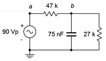
The first thing to do is to find the capacitive reactance.
\[X_C =− j \frac{1}{2 \pi f C} \nonumber \]
\[X_C =− j \frac{1}{2 \pi 100 Hz 75 nF} \nonumber \]
\[X_C \approx − j 21.22 k\Omega \nonumber \]
This reactance is in parallel with the 27 k\(\Omega\) resistor. Their combination is:
\[Z_{rc} = \frac{R\times jX_C}{R − jX_C} \nonumber \]
\[Z_{rc} = \frac{27 k\Omega \times (− j 21.22 k \Omega )}{27 k\Omega − j 21.22 k\Omega} \nonumber \]
\[Z_{rc} \approx 16.68E3\angle −51.8^{\circ} \Omega \nonumber \]
This impedance forms a voltage divider with the 27 k\(\Omega\) resistor to create \(v_b\).
\[v_b = e_{source} \frac{Z_{rc}}{R+Z_{rc}} \nonumber \]
\[v_b = 90 \angle 0^{\circ} V \frac{16.68E3\angle −51.8\Omega}{47k \Omega +16.68E3\angle −51.8 ^{\circ} \Omega} \nonumber \]
\[v_b \approx 25.5\angle −38.9^{\circ} V \nonumber \]
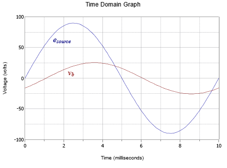
A time domain plot of \(v_b\) and the source voltage is shown in Figure \(\PageIndex{3}\).
Computer Simulation
To verify the results of the prior example, the circuit of Figure \(\PageIndex{2}\) is entered into a simulator as shown in Figure \(\PageIndex{4}\).
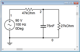
A time domain or transient analysis is run, examining \(v_b\) and the source voltage. Node 2 corresponds to \(v_b\). The results are shown in Figure \(\PageIndex{5}\).
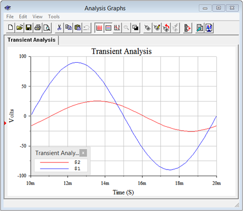
The plot is delayed one full cycle in order to get past the initial turn-on transient. The resulting amplitudes and phase shift line up perfectly with the plot of theoretical values in Figure \(\PageIndex{3}\).
Example \(\PageIndex{2}\)
For the circuit of Figure \(\PageIndex{2}\), determine \(v_{ab}\).
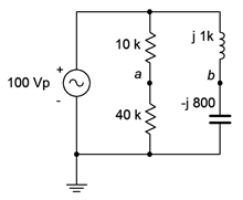
This circuit can be analyzed as a pair of voltage dividers. By definition, \(v_{ab} = v_a − v_b\). Numbering the resistors from top to bottom gives us:
\[v_a = e_{source} \frac{R_2}{R_1+R_2} \nonumber \]
\[v_a = 100\angle 0^{\circ} V \frac{40 k \Omega}{10k \Omega +10 k\Omega} \nonumber \]
\[v_a = 80 \angle 0^{\circ} V \nonumber \]
\[v_b = e_{source} − \frac{j X_C}{− jX_C+jX_L} \nonumber \]
\[v_b = 100\angle 0^{\circ} V \frac{− j 800\Omega}{− j 800 \Omega + j 1 k\Omega} \nonumber \]
\[v_b = 400\angle 180^{\circ} V \nonumber \]
This may also be written as \(−400\angle 0^{\circ} \). Now we subtract the two voltages to find \(v_{ab}\).
\[v_{ab} = v_a −v_b \nonumber \]
\[v_{ab} = 80 \angle 0^{\circ} V −400\angle 180^{\circ} V \nonumber \]
\[v_{ab} = 480\angle 0^{\circ} V \nonumber \]
Note that \(v_{ab}\) is nearly five times larger than the source voltage. This is mostly due to the fact that \(v_b\) itself is four times the source magnitude. Due to the fact that \(X_L\) and \(X_C\) are relatively close in size, they largely cancel each other when placed in series. This produces a small net reactance which creates a large current. This considerable current then produces large voltages across these components. The closer the magnitudes of \(X_L\) and \(X_C\), the higher the \(L\) and \(C\) component voltages. We will examine this effect in detail when we discuss resonance in Chapter 8.
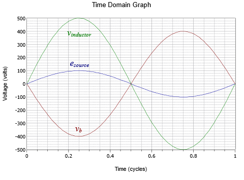
To verify this result, we can calculate the voltage across the inductor and check to see if KVL is satisfied.
\[v_{inductor} = e_{source} \frac{j X_L}{− jX_C+jX_L} \nonumber \]
\[v_{inductor} = 100\angle 0^{\circ} V \frac{j 1k \Omega}{− j 800 \Omega + j 1k \Omega} \nonumber \]
\[v_{inductor} = 500\angle 0^{\circ} V \nonumber \]
Adding the \(v_b\) of \(−400\angle 0^{\circ}\) volts to \(v_{inductor}\) does indeed yield the source voltage of \(100\angle 0^{\circ}\) volts.
This can be seen graphically in Figure \(\PageIndex{7}\). First, note that the inductor voltage is in phase with the source voltage. This is because the LC branch appears to be net inductive, producing a current lagging the source voltage by 90 degrees. This same current flows through the inductor, meaning its voltage leads this current by 90 degrees, and thus the inductor voltage is in phase with the source voltage. The lagging current also flows through the capacitor which produces a further 90 degree lag for the capacitor voltage (i.e., \(v_b\)) or 180 degrees total. Combining the large inductor voltage with a capacitor voltage that is nearly as large but effectively inverted yields the smaller source voltage.
Example \(\PageIndex{3}\)
In the circuit of Figure \(\PageIndex{8}\), determine the current flowing down through the inductor. Use the source as the reference (\(\angle 0^{\circ}\)).
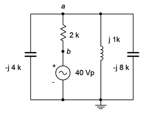
One possible approach for this is to find the equivalent total impedance that the source drives in order to find the source current. A current divider can then be used between the inductor and the pair of capacitors (all three being in parallel). Another option would be to find the impedance of the three reactive components and then use the voltage divider rule to find \(v_a\).
Once \(v_a\) is found, the inductor current can be found using Ohm's law. Each of these solution paths requires about as much work as the other so there is no clear preference. As we just used the voltage divider rule in the prior example, let's use the current divider rule this time.
We are going to need the combined capacitive reactance for the current divider, and we will also need it to find the total impedance, so let's do that first.
\[X_{Ctotal} = \frac{1}{\frac{1}{X_{C1}} + \frac{1}{X_{C2}}} \nonumber \]
\[X_{Ctotal} = \frac{1}{\frac{1}{− j 4 k\Omega} + \frac{1}{− j 8k \Omega}} \nonumber \]
\[X_{Ctotal} = 2667\angle −90^{\circ} \Omega \nonumber \]
This value is in parallel with the inductive reactance, and that combo is in series with the resistor, yielding the total impedance.
\[Z_{CL} = \frac{1}{\frac{1}{X_{Ctotal}} + \frac{1}{X_L}} \nonumber \]
\[Z_{CL} = \frac{1}{\frac{1}{− j 2667\Omega} + \frac{1}{j 1k \Omega}} \nonumber \]
\[Z_{CL} = 1600\angle 90^{\circ} \Omega \nonumber \]
\[Z_{total} = R+Z_{CL} \nonumber \]
\[Z_{total} = 2 k\Omega +1600\angle 90^{\circ} \Omega \nonumber \]
\[Z_{total} = 2561\angle 38.7^{\circ} \Omega \nonumber \]
The source current is found using Ohm's law.
\[i_{source} = \frac{e_{source}}{Z_{total}} \nonumber \]
\[i_{source} = \frac{40\angle 0^{\circ} V}{2561\angle 38.7^{\circ} \Omega} \nonumber \]
\[i_{source} = 15.6E-3\angle −38.7^{\circ} A \nonumber \]
We now apply a current divider between \(X_{Ctotal}\) and the inductor.
\[i_{inductor} = i_{source} \frac{X_{Ctotal}}{X_{Ctotal}+X_L} \nonumber \]
\[i_{inductor} = 15.6E-3\angle −38.7^{\circ} A \frac{− j 2667\Omega}{− j 2667\Omega +j 1000\Omega} \nonumber \]
\[i_{inductor} = 24.99E-3\angle −38.7^{\circ} A \nonumber \]
Once again we see a branch current that is larger in magnitude than the source current. This current should produce an inductor voltage of
\[v_{inductor} = i_{inductor} \times X_L \nonumber \]
\[v_{inductor} = 24.99E-3\angle −38.7 ^{\circ} A\times 1000\angle 90 ^{\circ} \Omega \nonumber \]
\[v_{inductor} = 24.99 \angle 51.3^{\circ} V \nonumber \]
The voltage across the resistor is
\[v_R = i_{source} \times R \nonumber \]
\[v_R =15.6E-3 \angle −38.7^{\circ} A \times 2000\angle 0^{\circ} \Omega \nonumber \]
\[v_R = 31.2\angle −38.7^{\circ} V \nonumber \]
KVL indicates that the sum of \(v_R\) and \(v_{inductor}\) should equal the source of \(40\angle 0^{\circ}\) volts, and it does (within rounding limits).
It is now time for some examples that use current sources.
Example \(\PageIndex{4}\)
Determine \(v_a\), \(v_b\) and \(v_{ab}\) in the circuit of Figure \(\PageIndex{9}\). Use the source as the reference angle of 0 degrees.
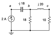
To find \(v_b\) we can determine the equivalent impedance of the two resistors and the inductor and multiply it by the source current. The rightmost resistor and inductor are in series, yielding \(10 + j20 \Omega\). This is in parallel with the 18 \(\Omega\) resistor.
\[Z_b = \frac{R_1\times Z_{LR}}{R_1 +Z_{LR}} \nonumber \]
\[Z_b = \frac{18\Omega \times (10+j 20 \Omega )}{18\Omega +(10+j 20 \Omega )} \nonumber \]
\[Z_b = 11.7\angle 27.9^{\circ} \Omega \nonumber \]
\[v_b = i_{source} \times Z_b \nonumber \]
\[v_b = 2\angle 0^{\circ} A\times 11.7 \angle 27.9^{\circ} \Omega \nonumber \]
\[v_b = 23.4 \angle 27.9^{\circ} V \nonumber \]
The voltage across the capacitor is \(v_{ab}\). We can find this through Ohm's law. Given the reference direction of the current source, the capacitor's voltage reference polarity is + to − from left to right.
\[v_{ab} = i_{source} \times X_C \nonumber \]
\[v_{ab} = 2\angle 0^{\circ} A\times 18\angle −90^{\circ} \Omega \nonumber \]
\[v_{ab} = 36\angle −90^{\circ} V \nonumber \]
Finally, \(v_a\) is just \(v_{ab}\) plus \(v_b\) based on KVL.
\[v_{a} = v_{ab} + v_b \nonumber \]
\[v_{a} = 36 \angle −90^{\circ} V+23.4 \angle 27.9^{\circ} V \nonumber \]
\[v_{a} = 32.48\angle −50.5^{\circ} V \nonumber \]
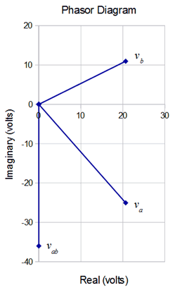
A phasor diagram is shown in Figure \(\PageIndex{10}\). Graphically, it can be seen that subtracting \(v_b\) from \(v_a\) yields \(v_{ab}\), as expected. Remember, this is a seriesparallel circuit and therefore we do not see necessarily 0 degree or 90 degree angles between the various voltages as found in simple series-only circuits.
Example \(\PageIndex{5}\)
For the circuit of Figure \(\PageIndex{11}\), determine \(v_b\) if the 1 amp source is used as the reference (\(\angle 0^{\circ}\)) and the 3 amp source has a \(30^{\circ}\) lagging phase angle.
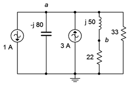
The two current sources are in parallel and can be combined together. We must be a little careful regarding polarity, though. First of all, a “\(30^{\circ}\) lagging phase angle” means that the second source is \(3\angle −30^{\circ}\) amps. Along with this, its reference direction is opposite that of the first source. This means that the second source is negative or inverted by 180 degrees relative to source one. Thus, we can treat it as a downward source of \(−3\angle −30^{\circ}\) amps, or \(3\angle 150^{\circ}\) amps, whichever we prefer. Now that they're both configured as having a downward reference direction, we simply add them together.
\[i_{total} = i_1+i_2 \nonumber \]
\[i_{total} = 1\angle 0^{\circ} A+3\angle 150^{\circ} A \nonumber \]
\[i_{total} = 2.192\angle 136.8^{\circ} A \nonumber \]
Alternately, we could subtract \(3\angle −30^{\circ}\) amps from the first source based on the reference directions, and note that the resulting direction of the combination is the same as that of the first source. Another option would be to reverse the reference direction of the first source. This would yield an upward direction with a value of \(2.192\angle −43.2^{\circ}\) amps.
Having simplified the circuit to a single current source, it should be obvious that the inductor is in series with the 22 \(\Omega\) resistor, and that combination is in parallel with both the capacitor and the 33 \(\Omega\) resistor. Finding that parallel impedance would allow us to find \(v_a\). Knowing \(v_a\), a voltage divider between the series inductor/resistor combo will yield \(v_b\). An important thing to note is that, given the downward reference direction of the equivalent current source, KCL indicates that the current direction through the other components must be upward, meaning that both \(v_a\) and \(v_b\) negative with respect to ground.
\[Z_{total} = \frac{1}{\frac{1}{X_C} + \frac{1}{R_1 + X_L} + \frac{1}{R_2}} \nonumber \]
\[Z_{total} = \frac{1}{\frac{1}{− j 80\Omega} + \frac{1}{22 \Omega +j 50 \Omega} + \frac{1}{33\Omega}} \nonumber \]
\[Z_{total} = 26.38\angle 6.45^{\circ} \Omega \nonumber \]
\[v_a =−i_{total} \times Z_{total} \nonumber \]
\[v_a =−2.192\angle 136.8^{\circ} A\times 26.38\angle 6.45^{\circ} \Omega \nonumber \]
\[v_a = 57.8\angle −36.8^{\circ} V \nonumber \]
If we had reversed the reference direction of the current source, using \(2.192\angle −43.2^{\circ}\) amps instead, the leading minus sign would not be required and we would arrive at the same result. Continuing,
\[v_b = v_a \left( \frac{R_1}{R_1+X_L} \right) \nonumber \]
\[v_b = 57.8\angle −36.8^{\circ} V \frac{22\Omega}{22\Omega +j 50\Omega} \nonumber \]
\[v_b = 23.29\angle −103^{\circ} V \nonumber \]
Analysis Across the Frequency Domain
For the most part, we have examined the response of a circuit to a single frequency of excitation. In many electronic systems, such as in the field of communications, numerous frequencies are present simultaneously. Recall from Chapter 1 how complex wave shapes such as square waves, triangle waves or music signals can be built from a series of sine waves. In such systems, the reactive components behave as different values to the various frequencies simultaneously. For example, a capacitor may have a reactance of \(−j400 \Omega \) for a 100 Hz signal while at the same time offering a reactance of \(−j40 \Omega \) for a 1 kHz signal. It is this dynamic quality that allows us to design circuits to suppress or block certain frequency components, or to select specific frequencies from a large range or spectrum of frequency components.
We shall introduce this concept by first analyzing the circuit at a couple of specific frequencies and then employ a simulator to perform a frequency domain analysis (sometimes called an AC analysis) to plot complex response curves of voltage versus frequency. The concept of frequency domain response will be expanded in upcoming work, particularly in Chapter 10.
Example \(\PageIndex{6}\)
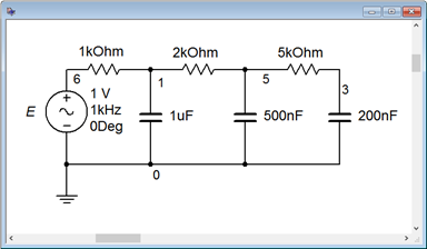
Consider the circuit shown in Figure \(\PageIndex{12}\). Assume the source is a one volt peak sine wave. Determine voltages \(v_a\), \(v_b\) and \(v_c\) if the source frequency is 10 kHz. Repeat this for an input frequency of 10 Hz.
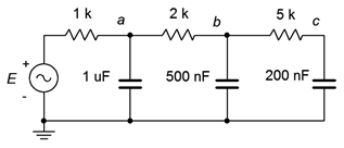
If we treat \(E\) as the input and \(v_c\) as the final output, this circuit behaves as a series of cascading frequency-dependent voltage dividers. Generally speaking, at low frequencies the capacitive reactances will be larger than the associated resistors, and most of the input voltage will make it to node \(c\). At high frequencies, the capacitive reactances will be small resulting in considerable voltage division at each node. Thus, only a small percentage of the input will make it to the final output. In other words, this circuit will filter out or remove high frequencies from the input with considerable effect, much more so than a single RC network.
First, we need to find the three capacitive reactances at 10 kHz. Starting at the left, we find
\[X_C =− j \frac{1}{2 \pi f C} \nonumber \]
\[X_C =− j \frac{1}{2 \pi 10Hz 1\mu F} \nonumber \]
\[X_C \approx − j 15.92 \Omega \nonumber \]
The other capacitive reactances work out to \(−j31.83 \Omega \) and \(−j79.58 \Omega \). The voltage \(v_a\) can be determined by a voltage divider between the 1 k\(\Omega\) resistor and the series-parallel combination of the remaining five components. First, the 5 k\(\Omega\) is in series with the 200 nF. That combination is in parallel with the 500 nF, which is in turn in series with the 2 k\(\Omega\) resistor. Finally, that group of four is in parallel with the 1 \(\mu\)F capacitor.
The resistors and capacitors are numbered from left to right in the equations following. We will need each of the segment impedances for subsequent calculations.
\[Z_{right3} = \frac{1}{\frac{1}{X_{C2}} + \frac{1}{Z_{right2}}} \nonumber \]
\[Z_{right3} = \frac{1}{\frac{1}{− j31.83\Omega} + \frac{1}{5000 − j 79.58 \Omega}} \nonumber \]
\[Z_{right3} = 31.83\angle −89.6^{\circ} \Omega \nonumber \]
\[Z_{right4} = R_2+Z_{right3} \nonumber \]
\[Z_{right4} = 2000\Omega +31.83\angle −89.6^{\circ} \Omega \nonumber \]
\[Z_{right4} = 2000\angle −0.91^{\circ} \Omega \nonumber \]
\[Z_{right5} = \frac{1}{\frac{1}{X_{C1}} + \frac{1}{Z_{right4}}} \nonumber \]
\[Z_{right5} = \frac{1}{\frac{1}{− j 15.92 \Omega} + \frac{1}{2000\angle −.91^{\circ} \Omega}} \nonumber \]
\[Z_{rightt} = 15.92\angle −89.5^{\circ} \Omega \nonumber \]
At last we come to \(v_a\):
\[v_a = e_{source} \frac{Z_{right5}}{R_1+Z_{right5}} \nonumber \]
\[v_a = 1\angle 0^{\circ} V \frac{15.92\angle −89.5^{\circ} \Omega}{1000\Omega +15.92\angle −89.5^{\circ} \Omega} \nonumber \]
\[v_a = 15.92\angle −88.6^{\circ} mV \nonumber \]
To find \(v_b\) we perform a voltage divider between the 2 k\(\Omega\) resistor and \(Z_{right3}\) using \(v_a\) as the input.
\[v_b = v_a \frac{Z_{right3}}{R_2+Z_{right3}} \nonumber \]
\[v_b = 15.92\angle −88.6^{\circ} mV \frac{31.83\angle −89.6^{\circ} \Omega}{2000\Omega +31.83\angle −89.6^{\circ} \Omega} \nonumber \]
\[v_b = 253.3\angle −177.3 ^{\circ} \mu V \nonumber \]
Finally, to find \(v_c\) we perform a voltage divider between the 5 k\(\Omega\) resistor and 200 nF capacitor using \(v_b\) as the input.
\[v_c = v_b \frac{X_{C3}}{R_3+X_{C3}} \nonumber \]
\[v_c = 253.3\angle −177.3^{\circ} \mu V \frac{− j 79.58\Omega}{5000\Omega − j 79.58\Omega} \nonumber \]
\[v_c = 4.03\angle 93.6^{\circ} \mu V \nonumber \]
Obviously, only a tiny percentage of the source signal is found at node \(c\) at this frequency.
Repeating this process at 10 Hz yields capacitive reactances of \(−j15.92 k\Omega\), \(−j31.83 k\Omega \) and \(−j79.58 k\Omega \). At this level, the amount of signal lost through each segment is inconsequential. For example, for the final segment the voltage divider ratio works out to:
\[\frac{v_c}{v_b} = \frac{X_{C3}}{R_3+X_{C3}} \nonumber \]
\[\frac{v_c}{v_b} = \frac{− j 79.58 k \Omega}{5000\Omega − j 79.58 k \Omega } \nonumber \]
\[\frac{v_c}{v_b} = 0.998\angle −3.6^{\circ} \nonumber \]
In other words, a mere 0.2% of the signal is lost and there is a modest \(−3.6^{\circ}\) phase shift. The results at the other nodes are similar and left as an exercise. Thus we see that that the low frequencies are allowed through this network while the high frequencies are attenuated.
Computer Simulation
While the results of Example \(\PageIndex{6}\) should be convincing as to the performance of the circuit, it should also be obvious that determining the voltages for any set of source frequencies would be a tedious exercise. Fortunately, there are other techniques that may be employed, such as those examined in Chapter 10. For now, though, we will turn our attention to a simulator. Most simulators offer an AC analysis or frequency domain analysis that will create two linked graphs; one for the voltage magnitude and another for the phase. We begin by entering the circuit of Figure \(\PageIndex{12}\) into a simulator as shown in Figure \(\PageIndex{13}\). Even though the schematic shows a 1 kHz source frequency, the AC analysis will allow us to specify the starting and ending frequencies for the plots. In this case, we'll use the 10 Hz and 10 kHz points specified in the example. The results are shown in Figure \(\PageIndex{14}\).
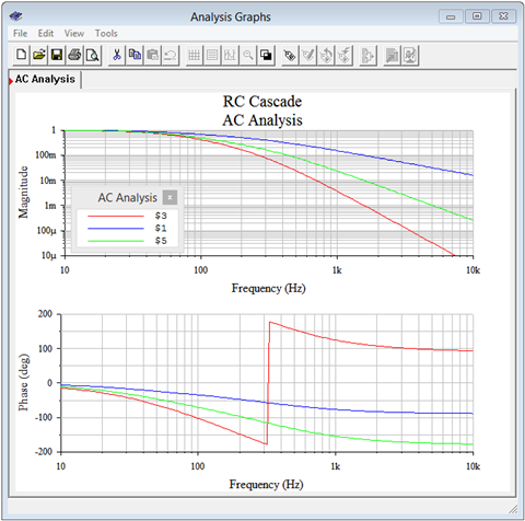
The top graph plots the voltages at nodes \(a\), \(b\) and \(c\) across frequency. It is obvious that, as the frequency increases, the voltage at each node decreases. The lower graph plots the phase shift at each of the nodes and it is apparent that the phase shift increases in the negative direction as frequency is increased. This is expected because, as the frequency increases, the capacitive reactance decreases, making each parallel combination appear more capacitive, and approaching −90 degrees each. A quick check of the voltage magnitudes and phases at 10 Hz indicates that very little signal is lost at the three node and that the phase shifts are close to zero. Further, at 10 kHz, there is considerable signal loss through each section, with each section producing nearly −90 degrees, just as calculated. Perhaps the only curious bit here is the abrupt change in phase shift shown at node \(c\) around 300 Hz (red trace). This is just an artifact of the plotting software. If an angle goes beyond \(\pm\)180 degrees, the value is rotated back the other way to keep the value within \(\pm\)180. For instance, −185 degrees is the same as +175 degrees.
Combining reactive elements can be a very effective means of selecting out a certain range of frequencies, as further illustrated in the following example.
Example \(\PageIndex{7}\)
In Chapter 2 we introduced the concept of a loudspeaker crossover network. The idea was to “steer” low frequencies to the woofer (low frequency transducer) and high frequencies to the tweeter (high frequency transducer). An advancement on that simple system is to use a combination of capacitors and inductors in place of a simple RC or RL network. One possible configuration is illustrated in Figure \(\PageIndex{15}\). At high frequencies, the capacitive reactance will be small while the inductive reactance will be large. Thus, virtually all of the input signal will reach the loudspeaker. In contrast, at low frequencies the capacitive reactances will be large and the inductive reactance small, resulting in hardly any of the input signal reaching the loudspeaker. Somewhere in the middle, a significant portion of the signal will make it through. This point is referred to as the crossover frequency. If the source voltage is 1 volt peak, determine the voltage developed across an 8 \(\Omega\) loudspeaker at a frequency of 2.6 kHz for this circuit.
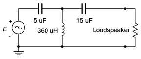
First, we need to determine the reactances at the frequency of interest.
\[X_{C1} =− j \frac{1}{2\pi f C} \nonumber \]
\[X_{C1} =− j \frac{1}{2\pi 2.6kHz 5\mu F} \nonumber \]
\[X_{C1} \approx − j12.24 \Omega \nonumber \]
The second capacitor is three times as large and therefore its reactance will be one-third as much, or \(−j4.08 \Omega \). For the inductor,
\[X_L = j 2\pi f L \nonumber \]
\[X_L = j 2\pi 2.6 kHz 360\mu H \nonumber \]
\[X_L\approx j 5.88\Omega \nonumber \]
Now that we have the reactances, the loudspeaker voltage can be computed via a pair of voltage dividers. In order find the loudspeaker voltage we'll first find the voltage developed across the inductor. To find that, we need to find the combined impedance of the three components on the right.
\[Z_{right3} = \frac{1}{\frac{1}{X_L} + \frac{1}{Z_{right2}}} \nonumber \]
\[Z_{right3} = \frac{1}{\frac{1}{j 5.88\Omega} + \frac{1}{8 − j 4.08\Omega}} \nonumber \]
\[Z_{right3} = 6.44\angle 50.3^{\circ} \Omega \nonumber \]
Now for the voltage divider to find \(v_{inductor}\).
\[v_{inductor} = e_{source} \frac{Z_{right3}}{Z_{right3} + X_{C1}} \nonumber \]
\[v_{inductor} = 1\angle 0^{\circ} V \frac{6.44\angle 50.3^{\circ} \Omega}{ 6.44 \angle 50.3^{\circ} \Omega − j 12.24 \Omega} \nonumber \]
\[v_{inductor} = 0.77\angle 110.8^{\circ} V \nonumber \]
And now the final voltage divider to find \(v_{loudspeaker}\).
\[v_{loudspeaker} = v_{inductor}\frac{Z_{loudspeaker}}{Z_{loudspeaker}+X_{C2}} \nonumber \]
\[v_{loudspeaker} = 0.77\angle 110.8^{\circ} \mu V \frac{8\Omega}{ 8\Omega − j 4.08\Omega} \nonumber \]
\[v_{loudspeaker} = 0.686\angle 137.9 ^{\circ} V \nonumber \]
At this particular frequency the loudspeaker sees about 2/3rds of the source voltage. For any higher frequency, the loudspeaker will see a larger share of the 1 volt source and for any lower frequency, the loudspeaker see less. At very low frequencies, only a few microvolts may get through.
Computer Simulation
In order to get a better sense of the loudspeaker voltage as a function of frequency, the circuit of Figure \(\PageIndex{15}\) is captured in a simulator as shown in Figure \(\PageIndex{16}\).
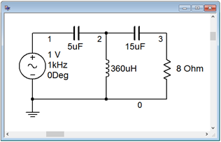
An AC analysis simulation is performed with the output shown in Figure \(\PageIndex{17}\).
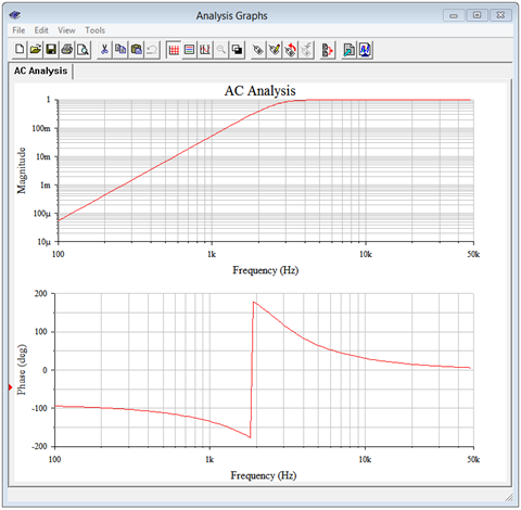
Both the magnitude and phase plots corroborate the calculated loudspeaker voltage at 2.6 kHz. The magnitude plot shows that the loudspeaker voltage is very close to the input level at frequencies above about 3 kHz. Below this frequency, the loudspeaker voltage rolls off considerably. Down at 100 Hz, well into the bass region, less than 100 microvolts, or under 0.01% of the input, reaches the loudspeaker. This circuit would make for an effective crossover network to a high frequency tweeter.
In closing, it is worth noting that a loudspeaker exhibits a complex impedance instead of simple resistive value, however, modeling it as an 8 \(\Omega\) resistor is sufficient to illustrate the operation of this circuit. We will take a closer look at the impedance of loudspeakers and other devices in upcoming chapters.