
7.2: Power Waveforms
- Page ID
- 25280

\( \newcommand{\vecs}[1]{\overset { \scriptstyle \rightharpoonup} {\mathbf{#1}} } \)
\( \newcommand{\vecd}[1]{\overset{-\!-\!\rightharpoonup}{\vphantom{a}\smash {#1}}} \)
\( \newcommand{\id}{\mathrm{id}}\) \( \newcommand{\Span}{\mathrm{span}}\)
( \newcommand{\kernel}{\mathrm{null}\,}\) \( \newcommand{\range}{\mathrm{range}\,}\)
\( \newcommand{\RealPart}{\mathrm{Re}}\) \( \newcommand{\ImaginaryPart}{\mathrm{Im}}\)
\( \newcommand{\Argument}{\mathrm{Arg}}\) \( \newcommand{\norm}[1]{\| #1 \|}\)
\( \newcommand{\inner}[2]{\langle #1, #2 \rangle}\)
\( \newcommand{\Span}{\mathrm{span}}\)
\( \newcommand{\id}{\mathrm{id}}\)
\( \newcommand{\Span}{\mathrm{span}}\)
\( \newcommand{\kernel}{\mathrm{null}\,}\)
\( \newcommand{\range}{\mathrm{range}\,}\)
\( \newcommand{\RealPart}{\mathrm{Re}}\)
\( \newcommand{\ImaginaryPart}{\mathrm{Im}}\)
\( \newcommand{\Argument}{\mathrm{Arg}}\)
\( \newcommand{\norm}[1]{\| #1 \|}\)
\( \newcommand{\inner}[2]{\langle #1, #2 \rangle}\)
\( \newcommand{\Span}{\mathrm{span}}\) \( \newcommand{\AA}{\unicode[.8,0]{x212B}}\)
\( \newcommand{\vectorA}[1]{\vec{#1}} % arrow\)
\( \newcommand{\vectorAt}[1]{\vec{\text{#1}}} % arrow\)
\( \newcommand{\vectorB}[1]{\overset { \scriptstyle \rightharpoonup} {\mathbf{#1}} } \)
\( \newcommand{\vectorC}[1]{\textbf{#1}} \)
\( \newcommand{\vectorD}[1]{\overrightarrow{#1}} \)
\( \newcommand{\vectorDt}[1]{\overrightarrow{\text{#1}}} \)
\( \newcommand{\vectE}[1]{\overset{-\!-\!\rightharpoonup}{\vphantom{a}\smash{\mathbf {#1}}}} \)
\( \newcommand{\vecs}[1]{\overset { \scriptstyle \rightharpoonup} {\mathbf{#1}} } \)
\( \newcommand{\vecd}[1]{\overset{-\!-\!\rightharpoonup}{\vphantom{a}\smash {#1}}} \)
\(\newcommand{\avec}{\mathbf a}\) \(\newcommand{\bvec}{\mathbf b}\) \(\newcommand{\cvec}{\mathbf c}\) \(\newcommand{\dvec}{\mathbf d}\) \(\newcommand{\dtil}{\widetilde{\mathbf d}}\) \(\newcommand{\evec}{\mathbf e}\) \(\newcommand{\fvec}{\mathbf f}\) \(\newcommand{\nvec}{\mathbf n}\) \(\newcommand{\pvec}{\mathbf p}\) \(\newcommand{\qvec}{\mathbf q}\) \(\newcommand{\svec}{\mathbf s}\) \(\newcommand{\tvec}{\mathbf t}\) \(\newcommand{\uvec}{\mathbf u}\) \(\newcommand{\vvec}{\mathbf v}\) \(\newcommand{\wvec}{\mathbf w}\) \(\newcommand{\xvec}{\mathbf x}\) \(\newcommand{\yvec}{\mathbf y}\) \(\newcommand{\zvec}{\mathbf z}\) \(\newcommand{\rvec}{\mathbf r}\) \(\newcommand{\mvec}{\mathbf m}\) \(\newcommand{\zerovec}{\mathbf 0}\) \(\newcommand{\onevec}{\mathbf 1}\) \(\newcommand{\real}{\mathbb R}\) \(\newcommand{\twovec}[2]{\left[\begin{array}{r}#1 \\ #2 \end{array}\right]}\) \(\newcommand{\ctwovec}[2]{\left[\begin{array}{c}#1 \\ #2 \end{array}\right]}\) \(\newcommand{\threevec}[3]{\left[\begin{array}{r}#1 \\ #2 \\ #3 \end{array}\right]}\) \(\newcommand{\cthreevec}[3]{\left[\begin{array}{c}#1 \\ #2 \\ #3 \end{array}\right]}\) \(\newcommand{\fourvec}[4]{\left[\begin{array}{r}#1 \\ #2 \\ #3 \\ #4 \end{array}\right]}\) \(\newcommand{\cfourvec}[4]{\left[\begin{array}{c}#1 \\ #2 \\ #3 \\ #4 \end{array}\right]}\) \(\newcommand{\fivevec}[5]{\left[\begin{array}{r}#1 \\ #2 \\ #3 \\ #4 \\ #5 \\ \end{array}\right]}\) \(\newcommand{\cfivevec}[5]{\left[\begin{array}{c}#1 \\ #2 \\ #3 \\ #4 \\ #5 \\ \end{array}\right]}\) \(\newcommand{\mattwo}[4]{\left[\begin{array}{rr}#1 \amp #2 \\ #3 \amp #4 \\ \end{array}\right]}\) \(\newcommand{\laspan}[1]{\text{Span}\{#1\}}\) \(\newcommand{\bcal}{\cal B}\) \(\newcommand{\ccal}{\cal C}\) \(\newcommand{\scal}{\cal S}\) \(\newcommand{\wcal}{\cal W}\) \(\newcommand{\ecal}{\cal E}\) \(\newcommand{\coords}[2]{\left\{#1\right\}_{#2}}\) \(\newcommand{\gray}[1]{\color{gray}{#1}}\) \(\newcommand{\lgray}[1]{\color{lightgray}{#1}}\) \(\newcommand{\rank}{\operatorname{rank}}\) \(\newcommand{\row}{\text{Row}}\) \(\newcommand{\col}{\text{Col}}\) \(\renewcommand{\row}{\text{Row}}\) \(\newcommand{\nul}{\text{Nul}}\) \(\newcommand{\var}{\text{Var}}\) \(\newcommand{\corr}{\text{corr}}\) \(\newcommand{\len}[1]{\left|#1\right|}\) \(\newcommand{\bbar}{\overline{\bvec}}\) \(\newcommand{\bhat}{\widehat{\bvec}}\) \(\newcommand{\bperp}{\bvec^\perp}\) \(\newcommand{\xhat}{\widehat{\xvec}}\) \(\newcommand{\vhat}{\widehat{\vvec}}\) \(\newcommand{\uhat}{\widehat{\uvec}}\) \(\newcommand{\what}{\widehat{\wvec}}\) \(\newcommand{\Sighat}{\widehat{\Sigma}}\) \(\newcommand{\lt}{<}\) \(\newcommand{\gt}{>}\) \(\newcommand{\amp}{&}\) \(\definecolor{fillinmathshade}{gray}{0.9}\)Computation of power in AC systems is somewhat more involved than the DC case due to the phase between the current and voltage. It has been stated in prior work that power dissipation is characteristic of resistors, and that ideal inductors and capacitors do not dissipate power. We shall show precisely why this is the case by examining three distinct cases for AC circuits: purely resistive, purely reactive and complex impedance.
Resistive Load
First, consider the case of the purely resistive load, that is, a load with a phase angle of 0 degrees. To determine the power, we simply multiply the voltage by the current. Recall that the basic expression for a sine wave voltage without a DC offset is:
\[v(t) = V \sin (2\pi f t +\theta ) \nonumber \]
where
- \(v(t)\) is the voltage at some time \(t\),
- \(V\) is the peak value,
- \(f\) is the frequency,
- \(\theta \) is the phase shift.
We know that the current and voltage are always in phase for a resistor, and thus \(\theta \) is zero degrees. Thus, the expression for a sinusoidal current is similar, using \(I\) in place of \(V\) for the peak current. We multiply the current and voltage together to arrive at an expression for power1:
\[\begin{align} P(t) &= v(t)\times i(t) \\[4pt] &= V \sin (2\pi ft)\times I \sin (2\pi ft) \\[4pt] &= VI \left( \frac{1}{2} − \frac{1}{2} \cos (2\pi 2 ft) \right) \\[4pt] &= \frac{VI}{2} − \frac{VI}{2} \cos (2\pi 2 ft) \label{7.1} \end{align} \]
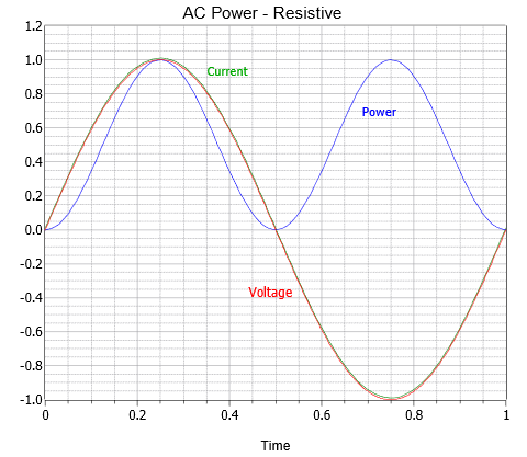
The final expression is made of two parts; the first portion which is fixed (not a function of time) and the second portion which consists of a negative cosine wave at twice the original frequency. This can be visualized as a time shifted sine wave that is riding on a DC level which is equal to the peak value of the new sinusoid. This is shown in Figure \(\PageIndex{1}\) using current and voltage peaks normalized to unity. In this figure, the current waveform (green) is drawn just slightly above its true value so that it may be seen easily next to the otherwise identical red voltage waveform.
The power product is shown in blue. Unless the frequency is ridiculously low, the resistor's heating will respond to the average value of this waveform thanks to the device's thermal time constant. Due to the fact that sinusoids are symmetrical around zero, the effective power dissipation averaged over time will be the offset value, or \(VI/2\). For example, a one volt peak source delivering a current of one amp peak, as shown here, should generate \(VI/2\), or 0.5 watts. This crosschecks nicely with the RMS calculation of roughly 0.707 volts RMS times 0.707 amps RMS also yielding 0.5 watts.
Reactive Load
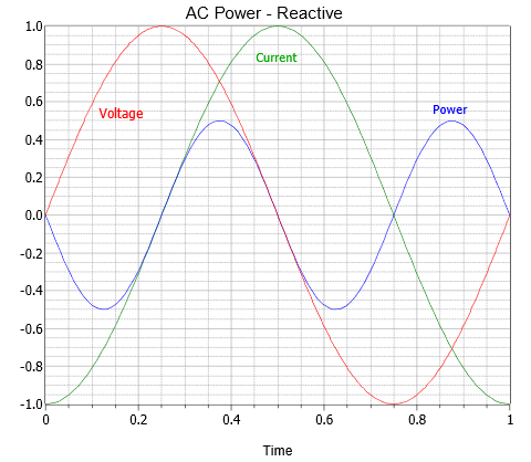
The situation is considerably different if the load is purely reactive. For a load consisting of just an inductor, the voltage leads the current by 90 degrees. This is equivalent to a cosine wave. Once again, we multiply the voltage by the current to arrive at an expression for power:
\[\begin{align} P(t) &= V \cos 2\pi ft\times I \sin 2\pi ft \\[4pt] &= VI \left( \frac{1}{2} \sin 2\pi 2 ft \right) \\[4pt] &= \frac{VI}{2} \sin 2\pi 2 ft \label{7.2} \end{align} \]
Note that this expression does not contain a constant term and only contains a time-varying term. Consequently, without an offset, there is no net power dissipation. The result is shown in Figure \(\PageIndex{2}\). Here power is being alternately generated and dissipated (i.e., positive values indicate dissipation while negative values indicate generation). In this respect, the reactive element can be thought of as alternately storing and releasing energy in the manner of an ideal spring being compressed and then released.
Complex Impedance Load
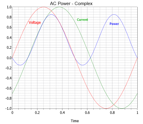
Finally, we come to the case of a complex load, part resistive and part reactive. Given some phase angle, \(\theta \), we have:
\[\begin{align} P(t) &= V \sin 2\pi ft\times I \sin (2\pi ft+\theta ) \\[4pt] &= VI \left( \frac{1}{2} \cos \theta − \frac{1}{2} \cos (2\pi 2 ft+\theta ) \right) \\[4pt] &= \frac{VI}{2} \cos \theta − \frac{VI}{2} \cos (2\pi 2 ft+\theta ) \label{7.3} \end{align} \]
This expression contains both a constant term and a time varying term, like the case for the purely resistive load shown in Equation \ref{7.1}. There is, however, an important distinction. The constant term is multiplied by the cosine of the impedance angle, a value whose magnitude ranges from 0 up to 1. Therefore, unless \(\theta \) is zero, the offset will not equal the peak value of the sinusoidal portion. This is a particularly important point which shall be amplified in a moment.
Example waveforms using \(\theta = 45^{\circ}\) are shown graphically in Figure \(\PageIndex{3}\). The power waveform dips slightly below zero but is not symmetrical around the time axis. Consequently, there is some power dissipation but not as much as in the purely resistive case. In short, the long term power average is now a function of the phase angle, \(\theta \). As cosine \(\theta \) may range between 0 and 1, the power for the complex impedance case will never be more than that of the purely resistive version. Indeed, we can see that Equation \ref{7.3} is the general case. If the load is purely resistive then \(\theta \) is zero, and Equation \ref{7.3} reduces to Equation \ref{7.1}. Similarly, if the load is purely reactive then \(\theta \) is \(\pm\)90 degrees, and Equation \ref{7.3} reduces to Equation \ref{7.2}.
While this analysis used an inductive load, the same can be said regarding the capacitive case (simply swap the labels for the current and voltage waveforms). Finally, in the equations above, \(V\) and \(I\) are peak values. If RMS values are used, there is no need to divide \(VI\) by 2.
At this point we can see that resistors dissipate true power but that reactive components do not. This raises a practical problem, namely, what to call the currentvoltage product for purely reactive or complex loads. That is, we can't lump together the current-voltage values for an inductor with those of a resistor any more than we would simply add the magnitudes of resistance and reactance. The practical solution is that we refer to the “power” in reactive components as reactive power. Reactive power uses the symbol Q. Further, the units are not watts, but volt-amps reactive, or more commonly, VAR2. Continuing, for a complex impedance we refer to apparent power. It uses the symbol S and has units of volt-amps, abbreviated VA. It is called apparent power because it appears to be the power if you naively multiply the value obtained from a voltmeter by the value obtained from an ammeter. Those devices would not account for the phase angle between the voltage and current, unlike a proper power meter, and their product would not be the true power. The various power terms are summarized in Figure \(\PageIndex{4}\).
| Quantity | Symbol | Unit, Abbreviation |
|---|---|---|
| Power | P | watts, W |
| Apparent Power | S | volt-amps, VA |
| Reactive Power | Q | volt-amps reactive, VAR |
A few examples are in order to help solidify these concepts.
Example \(\PageIndex{1}\)
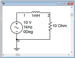
Determine the power dissipated by the resistor in the circuit of Figure \(\PageIndex{5}\). Also find the apparent power drawn by the circuit and the reactive power of the inductor. The source frequency is 1 kHz.
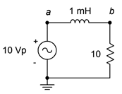
The first item is to find the reactance of the inductor.
\[X_L = 2\pi f L \nonumber \]
\[X_L = 2\pi 1 kHz 1 mH \nonumber \]
\[X_L = j 6.283 \Omega \nonumber \]
There are several ways to find power. In a series loop like this, the most direct is to use the \(i^2R\) forms. The source current can be found via Ohm's law. As power calculations utilize RMS values, first find the RMS value of the source voltage.
\[v_{RMS} = \frac{v_{peak}}{\sqrt{2}} \nonumber \]
\[v_{RMS} = \frac{ 10V}{\sqrt{2}} \nonumber \]
\[v_{RMS} \approx 7.07V \nonumber \]
\[i = \frac{v}{Z} \nonumber \]
\[i = \frac{7.07 V}{10+j 6.283\Omega} \nonumber \]
\[i = 0.5986\angle −32.1^{\circ} A \nonumber \]
For the power calculations, we shall only use the magnitudes of the voltage and current. Here, the symbol “\(| |\)” refers to just the magnitude of the reactance or impedance.
\[P = i^2 R \nonumber \]
\[P = (0.5986A)^2 10\Omega \nonumber \]
\[P \approx 3.58 W \nonumber \]
\[Q = i^2 | X | \nonumber \]
\[Q = (0.5986 A)^2 6.283\Omega \nonumber \]
\[Q \approx 2.25 \text{ VAR, inductive} \nonumber \]
\[S = i^2 | Z | \nonumber \]
\[S = (0.5986 A)^2 |10+j 6.283\Omega | \nonumber \]
\[S \approx 4.23 \text{ VA, inductive} \nonumber \]
Computer Simulation
The circuit of Figure \(\PageIndex{5}\) is captured in a simulator as shown in Figure \(\PageIndex{6}\). Three different transient analysis simulations are run.
The first simulation plots the circulating current (green), the resistor voltage (red) and their product (the power, in blue). This is shown in Figure \(\PageIndex{7}\). We can see that current and voltage are perfectly in phase, as expected. Also, the power waveform ranges from zero up to about 7 watts. The average of this is approximately half of the peak-to-peak, or about 3.5 watts, just as calculated.
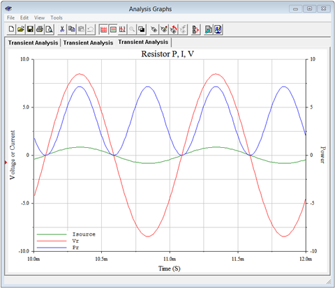
The power value can also be computed from voltage times current as a crosscheck. The voltage across the resistor can be found via the voltage rule, and its magnitude is approximately 5.986 volts RMS. Multiplying this by the RMS current will also yield 3.58 watts.
It is instructive to compare these curves to those generated in Figure \(\PageIndex{1}\) for the general resistive case. The current and voltage values in Figure \(\PageIndex{1}\) were normalized to unity so they do not appear to be identical to those of Figure \(\PageIndex{7}\), however, the important part is that the phase relationships are the same along with the position of the power waveform. In both cases the power waveform ranges from a minimum of zero up to some maximum value. Consequently, its average value must be half of its peak-to-peak value.
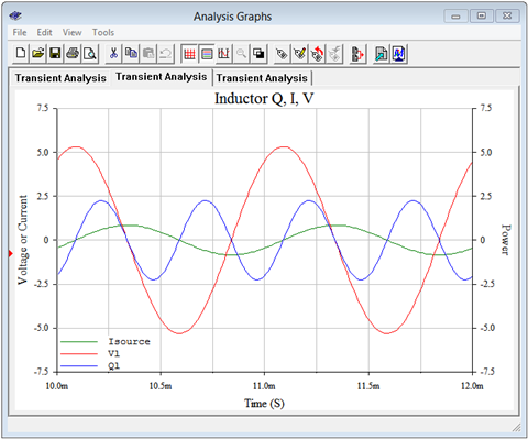
A second set of plots is generated for the inductor. This is shown in Figure \(\PageIndex{8}\). Again, compare this set against the curves seen in Figure \(\PageIndex{2}\) for the general reactive case. We can see that the current (green) is 90 degrees out of phase with the inductor's voltage (red) and lagging, as expected. More importantly, we see that the power waveform (blue) is centered around zero. The full cycle average of this is zero, meaning that no power is dissipated. But how does this square with the 2.25 VAR reactive power that was calculated for the inductor? A close look at the power plot shows that that value corresponds to the maximum value of the reactive power waveform (i.e., half of its peak-to-peak value).
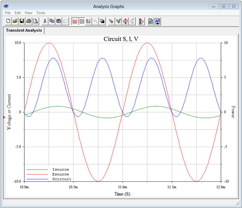
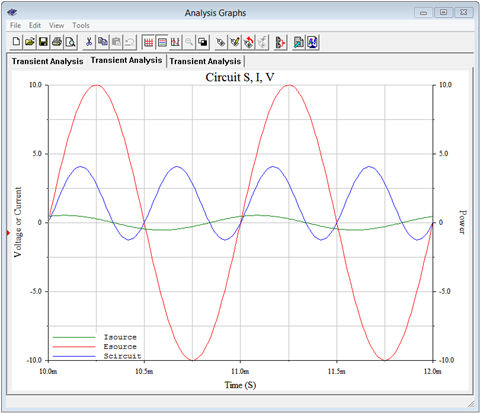
Finally, a third set of curves are created for the circuit as a whole. In other words, now we're treating the series combination of the inductor and resistor as the load. The results are illustrated in Figure \(\PageIndex{9}\).
The computed impedance phase angle was lagging at 32.1 degrees. We can see this same shift between the voltage (red) and current (green) waveforms. The interesting bit here is the offset and amplitude of the power waveform (blue). The waveform has a peak-to-peak value of about 8.5 VA. Once again, the computed value for apparent power, \(S\), works out to one-half of the plotted peak-to-peak value. This will be the case for \(P\), \(Q\) and \(S\). Further, it turns out that if we find the full cycle average of this waveform, those small negative peaks would subtract from the total area and reduce the value. The result would be the true power of 3.58 watts. We'll look at this more closely following another example.
Example \(\PageIndex{2}\)
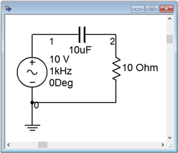
Determine the power dissipated by the resistor in the circuit of Figure \(\PageIndex{10}\). Also find the apparent power drawn by the circuit and the reactive power of the capacitor. The source frequency is 1 kHz.
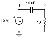
The first item is to find the reactance of the capacitor.
\[X_C = \frac{1}{2\pi f C} \nonumber \]
\[X_C = \frac{1}{2\pi 1kHz 1\mu F} \nonumber \]
\[X_C = − j 15.92\Omega \nonumber \]
Unlike the the previous example, we shall use the \(v^2 /R\) forms for power as an alternative. The RMS value of the source voltage is 7.07 volts. First, find \(v_R\).
\[v_R = E \frac{R}{R − jX_C} \nonumber \]
\[v_R = 7.07V \frac{10\Omega}{10 − j 15.92\Omega} \nonumber \]
\[v_R = 3.761\angle 57.9^{\circ} V \nonumber \]
The capacitor voltage is found via KVL:
\[v_C = E −v_R \nonumber \]
\[v_C = 7.07\angle 0^{\circ} −3.761\angle 57.9 ^{\circ} V \nonumber \]
\[v_C = 5.99\angle −32.1^{\circ} V \nonumber \]
For the powers, we just use the magnitude of the voltage.
\[P = \frac{v^2}{R} \nonumber \]
\[P = \frac{(3.761 V)^2}{10\Omega} \nonumber \]
\[P \approx 1.414W \nonumber \]
\[Q = \frac{i^2}{| X |} \nonumber \]
\[Q = \frac{(5.99 V)^2}{15.92\Omega} \nonumber \]
\[Q \approx 2.25 \text{ VAR, capacitive} \nonumber \]
\[S = \frac{E^2}{|Z |} \nonumber \]
\[S = \frac{(7.07 V)^2}{| 10 − j15.92 \Omega |} \nonumber \]
\[S \approx 2.66 \text{ VA, capacitive} \nonumber \]
Computer Simulation
In order to verify the results, the circuit of Figure \(\PageIndex{10}\) is captured in a simulator as shown in Figure \(\PageIndex{11}\). Once again, three different transient analysis simulations are run; one each for the resistor, the capacitor, and the pair together.
In Figure \(\PageIndex{12}\) we see the results of a transient analysis run on the resistor. We can see that the voltage and current are in phase. Also, the power waveform swings from zero up to around 2.8 watts or so. This corresponds to an average value of just under 1.5 watts, and this agrees nicely with the computed result.
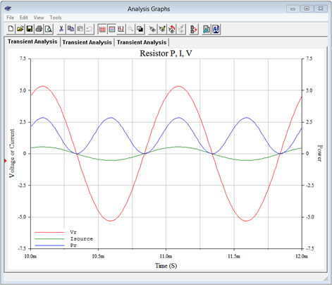
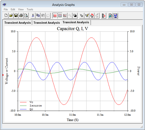
Figure \(\PageIndex{13}\) illustrates the results from a transient analysis run on the capacitor. As expected, the current is leading the voltage by 90 degrees. We can also see that the power waveform is swinging symmetrically around zero, meaning that there is no net power dissipation. The peak value is just under 2.5 VAR, aligning nicely with the calculated value.
Finally, in Figure \(\PageIndex{14}\) we have the results of a transient analysis using both the capacitor and the resistor as the load. The current waveform is still leading the voltage, but by less than 90 degrees. In fact, it leads by about 2/3rds of a division, some \(60^{\circ}\) or so, which conforms nicely to the expected impedance angle of \(−57.9^{\circ}\) (i.e. from \(10 − j15.92 \Omega \)). The power waveform sits slightly below the horizontal axis indicating it is neither true power nor reactive power, but a combination. The peak-to-peak value is somewhat over 5 units, indicating an apparent power of just over 2.5 VA, again, just as expected.
References
1A useful trigonometric identity here is \((\sin x)^2 = 1/2 - 1/2 \cos 2x\)
2For the plural form, some sources use “VARs” while others use “VAR”. We shall use the latter.