
3.2: Rectification
- Page ID
- 25397

Rectification is the process of turning an alternating current waveform into a direct current waveform, i.e., creating a new signal that has only a single polarity. In this respect it's reminiscent of the common definition of the word, for example where “to rectify the situation” means “to set something straight”. Before continuing, remember that a DC voltage or current does not have to exhibit a constant value (like a battery). All it means is that the polarity of the signal never changes. To distinguish between a fixed DC value and one that varies in amplitude in a regular fashion, the latter is sometimes referred to as pulsating DC.
The concept of rectification is crucial to the operation of modern electronic circuits. Most electronic devices such as a TV or computer require a fixed, unchanging DC voltage to power their internal circuitry. In contrast, residential and commercial power distribution is normally AC. Consequently, some form of AC to DC conversion is required1. This is where the asymmetry of the diode comes in.
3.2.1: Half-wave Rectification
To understand the operation of a single diode in an AC circuit, consider the diagram of Figure \(\PageIndex{1}\). This is a simple series loop consisting of a sine wave source, a diode and a resistor that serves as the load. That is, primarily we will be interested in the voltage developed across the resistor.
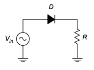
Figure \(\PageIndex{1}\): Basic AC diode-resistor circuit.
For positive portions of the input wave, the diode will be forward-biased. To a first approximation it will appear as a closed switch. Consequently, all of the input signal will drop across the resistor. In contrast, when the input signal switches to a negative polarity on the other half of the waveform, the diode will be reverse-biased. Therefore, the diode acts as an open switch. The circulating current drops to zero thereby producing no voltage across the resistor. All of the applied potential drops across the diode, as indicated by Kirchhoff's voltage law (KVL). The input and load resistor's voltage waveforms can be seen in Figure \(\PageIndex{2}\).
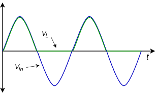
Figure \(\PageIndex{2}\): Half-wave rectification waveforms.
The resulting signal seen across the load resistor is a pulsating DC waveform. We have effectively removed the negative half of the waveform leaving just the positive portion. Because only half of the input waveform makes it to the load, this is referred to as half-wave rectification.
It is worth noting that if the AC peak input voltage is not particularly large, there can be an obvious discrepancy between the peak levels of the input and load signals. For example, if the peak input voltage is in the range of three or four volts and a silicon diode is used, the resulting waveforms would look more like Figure \(\PageIndex{3}\).
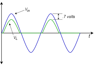
Figure \(\PageIndex{3}\): Half-wave rectification waveforms including forward diode drop.
In this case the 0.7 volt forward drop cannot be ignored as it represents a sizable percentage of the input peak. The positive pulses are also slightly narrowed as current will not begin to flow at reasonable levels until the input voltage reaches 0.6 to 0.7 volts.
If the diode was oriented in reverse, it would block the positive portion of the input and allow only the negative portion through. In this instance the load waveform would appear flipped top to bottom compared to Figures \(\PageIndex{2}\) and \(\PageIndex{3}\).
Computer Simulation
A simulation schematic for a simple half-wave rectifier is shown in Figure \(\PageIndex{4}\). A sine wave source of 10 volts peak is used to feed a popular 1N4000 series rectifier diode connected to a 100 \(\Omega\) load. The source frequency is 60 hertz, the North American standard for power distribution.
A transient analysis is run resulting in the waveforms shown in Figure \(\PageIndex{5}\). The source voltage waveform is shown in red while the load voltage waveform is depicted in blue. While the half-wave rectification is obvious, the loss due to the forward voltage drop of the diode is clearly evident. Based on the vertical scale, a value just under one volt would be a reasonable estimate. The simulation agrees nicely with the expected result as drawn in Figure \(\PageIndex{3}\), although not as extreme due to the increased source voltage.
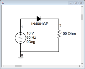
Figure \(\PageIndex{4}\): Simulation schematic for halfwave rectifier.
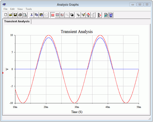
Figure \(\PageIndex{5}\): Transient analysis for halfwave rectifier.
On a practical note, there are still two items to consider when it comes to converting AC to DC. The first item is the issue of scaling the 120 VAC RMS outlet voltage to a more useful level. In many cases this means lowering the voltage although there are some applications such as high power amplifiers where the voltage will need to be increased. The second item involves smoothing the pulsating DC to produce a constant value, much like a battery.
3.2.2: A Note Regarding Transformers
The aforementioned voltage scaling issue can be addressed through the use of a transformer. While a complete exploration of transformers is beyond the scope of this chapter, we can present the basics. In simple terms, a transformer has an input side, or primary, and an output side, or secondary. Each side is made up of a coil of wire and these coils are wound around a common magnetic core. The current in the primary-side coil creates a magnetic flux in the core. This flux induces a current in the secondary coil. Ideally, the voltage is decreased and the current is increased by the ratio of the number of loops between these coils. For example, if the secondary-side coil has half as many turns as the primary-side coil then the secondary voltage will be half of the primary voltage and its current will be twice as large as the primary current. This implies that in the ideal case there is no power lost within the transformer. It simply transforms the power from high-voltage/low-current to low-voltage/high-current (or vice versa), hence the name. In reality, transformers do have voltage and current limits, and they are specified in terms of a volt-amp or VA rating which is simply the product of the nominal secondary voltage and maximum allowed secondary current. Transformers that decrease the voltage are referred to as step-down while those that increase the voltage are referred to as step-up. Finally, it is possible to create transformers with multiple primaries and secondaries (via either separate coils or multi-tapped coils). The resulting series and parallel coil configurations make them much more flexible.
3.2.3: Smoothing (Filtering) the Output
The second issue we have is smoothing and leveling the pulsating DC. The most straightforward method to achieve this is to add a capacitor in parallel with the load. The capacitor will charge up during the conduction phase, thus storing energy. When the diode turns off, the capacitor will begin to discharge, thus transferring its stored energy into the load. The larger the capacitor, the greater its storage capacity and the smoother the load voltage will be. It turns out that there is a down side to large capacitors, as we shall see. Consequently, the goal will not be to use as large of a capacitor as possible but rather to use an optimal size for a given application. A half-wave rectifier with transformer and capacitor is shown in Figure \(\PageIndex{6}\).
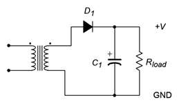
Figure \(\PageIndex{6}\): Half-wave rectifier with transformer and filter capacitor.
One way of looking at the inclusion of the smoothing capacitor is to consider that it, along with the load resistance, make up an \(RC\) discharge network. To achieve a smooth load voltage the discharge time constant should be much longer than the gap produced when the diode turns off. For 60 hertz operation, this gap is half of the period, or roughly 8.3 milliseconds. The time constant equation is
\[\tau = RC \nonumber \]
Recalling that in one time constant the capacitor voltage will fall to well below half of the starting value (roughly 37%), we will need a time constant several times larger than 8.3 milliseconds. For example, suppose our effective load resistance is 100 \(\Omega\). If we use a 1000 \(\mu\)F capacitor, the resulting time constant would be 100 milliseconds, or over ten times the gap duration. A much smaller capacitor, say around 50 \(\mu\)F, would not be nearly so effective at keeping the voltage constant.
The variation in output voltage due to capacitor discharge is referred to as ripple. It can be modeled as an AC voltage riding on a larger DC output. The magnitude of the ripple worsens as the load current increases. Under light load conditions, the output will tend to float to the peak voltage of the secondary with very little ripple. As load current demand goes up, the ripple magnitude increases and the nominal output voltage begins to drop.
Computer Simulation
Two variations on a filtered half-wave rectifier are simulated below. Both versions use a 100 \(\Omega\) load with a 10 volt source, similar to the prior simulation. The first version uses a 50 \(\mu\)F filter capacitor while the second ups this to 1000 \(\mu\)F. In both cases a 1 \(\Omega\) resistor is added in series with the capacitor to serve as a current sensor. The first version is shown in Figure \(\PageIndex{7}\).
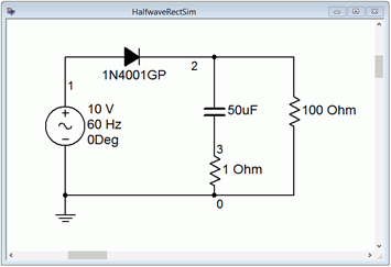
Figure \(\PageIndex{7}\): Simulation schematic for half-wave rectifier with 50 \(\mu\)F filter capacitor.
A transient analysis simulation graph is shown in Figure \(\PageIndex{8}\). The input waveform is colored blue while the load voltage is red. Comparing this waveform to that depicted in Figure \(\PageIndex{5}\) shows the effect of the capacitor stretching out the pulse and partially filling in the gap. It is obvious that this capacitor is too small given the load resistance and the resulting current demand. Indeed, by the time the next pulse arrives the capacitor is nearly depleted and the output voltage has dropped to around one volt.
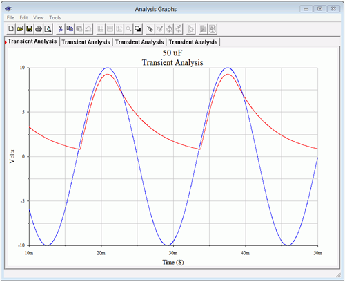
Figure \(\PageIndex{8}\): Transient analysis simulation for half-wave rectifier using a 50 \(\mu\)F filter capacitor.
In Figure \(\PageIndex{9}\) the simulation is rerun, but this time using a 1000 \(\mu\)F capacitor in place of the 50 \(\mu\)F. As expected, the increased \(RC\) time constant results in a much more stable load voltage. In this version the output has dropped from a little over nine volts to about eight volts yielding a peak-to-peak ripple of a volt and a half or so. The peak voltage of just over nine volts versus the applied ten volts is largely due to the voltage drop across the rectifying diode.
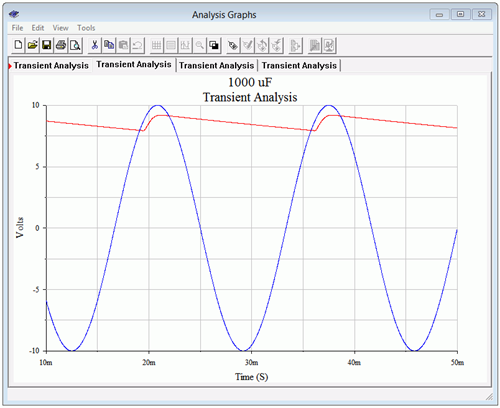
Figure \(\PageIndex{9}\): Transient analysis simulation for half-wave rectifier using a 1000 \(\mu\)F filter capacitor.
One thing that may not be apparent immediately is that the charge time for the larger capacitor is much shorter than for the smaller unit. This is perhaps counterintuitive. With a larger capacitor, the diode turns on for a shorter time because its cathode is held at a high voltage due to the capacitor. That is, it will only turn on when the input voltage exceeds the capacitor voltage by roughly 0.7 volts. It is only during this time that the capacitor will be replenished, and this can lead to very large current spikes.
To investigate this effect, the simulations are rerun, but this time adding the voltage across the 1 \(\Omega\) sensing resistor. This relatively small value will have only a modest effect on the charging and discharging, and conveniently scales to the current value (i.e., 100 millivolts signifies 100 milliamps). First, examine the transient simulation of Figure \(\PageIndex{10}\) using the 50 \(\mu\)F capacitor.
The red sweep is the output voltage while the blue sweep represents the capacitor current. The output voltage plot uses the left vertical axis while the current plot uses the right vertical axis. As the load voltage begins to rise, we see an abrupt spike in the capacitor current. This is current charging the capacitor and it peaks at about 180 milliamps. The total time for the charge phase is around 4 milliseconds. Once the output voltage peaks, the capacitor starts to discharge into the load. During the discharge phase note that the capacitor current's polarity has reversed. It is negative, peaking at roughly −80 milliamps, and delivering current to the load.
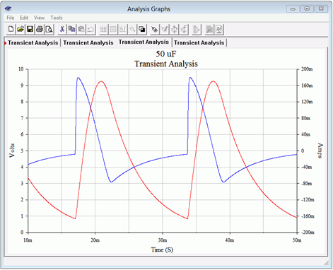
Figure \(\PageIndex{10}\): Transient analysis current waveform using a 50 \(\mu\)F filter capacitor.
This simulation is repeated using the 1000 \(\mu\)F capacitor. The results are shown in Figure \(\PageIndex{11}\).
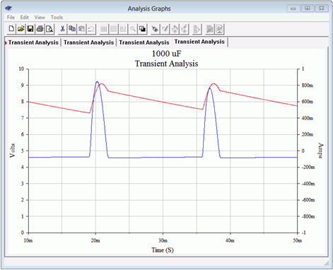
Figure \(\PageIndex{11}\): Transient analysis current waveform using a 1000 \(\mu\)F filter capacitor.
The blue current waveform peaks at approximately 800 milliamps, or over four times the value compared to using the smaller capacitor. Also, the width of the positive pulse has decreased to about 2.5 milliseconds. The discharge phase is nearly flat, implying that the output voltage must be more stable as this capacitor is the only source for load current during this phase.
3.2.4: Full-wave Rectification
An improvement on half-wave rectification is full-wave rectification. Half-wave rectification is inefficient because it essentially throws away the negative portion of the input. In contrast, full-wave rectification makes use of the negative portion by inverting or flipping its polarity. The resulting circuit is modestly larger and more complicated but results in large performance improvements. For example, filter capacitor size is greatly reduced.
There are two popular methods to achieve full-wave rectification. The first method uses a pair of diodes with a center-tapped (i.e., split) secondary. The second method uses a four diode bridge network. The diode bridge form is also capable of producing a bipolar output (i.e., a positive output along with a negative output, typically of the same magnitude).
The two diode center-tapped secondary circuit is shown in Figure \(\PageIndex{12}\). This schematic also includes the filter capacitor.
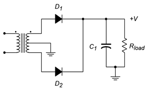
Figure \(\PageIndex{12}\): Full-wave center-tapped rectifier with capacitor.
The operation is as follows. During the positive half of the source voltage diode \(D_1\) is forward-biased while \(D_2\) is reverse-biased. Therefore the upper half of the secondary behaves like a simple half-wave rectifier allowing current to flow through \(D_1\) and into the load. Due to the reverse-bias on \(D_2\), the lower half presents an open circuit and is effectively removed. In mirror fashion, when the applied potential switches polarity \(D_1\) will be reverse-biased while \(D_2\) becomes forward-biased. Current is now free to flow through \(D_2\) into the load. Thus, both halves of the input waveform are used. The resulting waveforms are illustrated in Figure \(\PageIndex{13}\). For clarity, the filtering effect of the capacitor is not shown and \(V_{in}\) represents one half of the total secondary voltage.
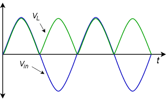
Figure \(\PageIndex{13}\): Full-wave rectifier waveforms.
An important point to remember about this configuration is that the load only “sees” half of the secondary at any given time. Therefore, the load voltage will only be half of the total secondary voltage (minus one forward diode drop). For example, if the transformer has a 10:1 turns ratio and is being fed from a standard 120 volt source, the secondary will produce 12 volts RMS. Ignoring the diode drop, the load would see half of this, or 6 volts RMS (about 8.5 volts peak). Typically, transformers are rated by their total secondary voltage so this transformer would be referred to as having a “12 volt center-tapped secondary”.
A four diode bridge rectifier is shown in Figure \(\PageIndex{14}\). A filter capacitor is included. Also, note the usage of a standard, non center-tapped secondary. As this is a very common configuration, the four diode bridge is available as a single four-lead part in a variety of sizes and current capacities.
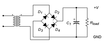
Figure \(\PageIndex{14}\): Full-wave bridge rectifier with capacitor.
The operation of this circuit is illustrated in Figure \(\PageIndex{15}\) for the positive portion of the input. First, current flows from the top of the secondary to the \(D_1/D_2\) junction. Only \(D_2\) offers a forward-bias path so current flows through \(D_2\) to the junction with \(D_4\) and the load. As \(D_4\) presents a reverse-bias path, current must flow down through the load. From ground, current continues to the \(D_1/D_3\) junction. Although at first glance it appears that current could flow through either diode, remember that the cathode of \(D_1\) is tied to the high side of the secondary. Therefore, its potential must be higher than the anode side, making it reverse-biased. Consequently, the current flows down through \(D_3\). A similar situation occurs at \(D_4\) and current is directed back to the low side of the secondary. In short, \(D_2\) and \(D_3\) are forward-biased while \(D_1\) and \(D_4\) are reverse-biased. The load sees the entire secondary voltage minus two forward diode drops.
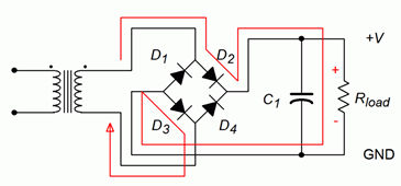
Figure \(\PageIndex{15}\): Full-wave bridge rectifier analysis, positive input.
During the negative polarity portion of the input the situation is reversed as illustrated in Figure \(\PageIndex{16}\). Current will flow from the bottom of the secondary through \(D_4\), down through the load, and finally back to the top of the secondary via \(D_1\). Thus, \(D_1\) and \(D_4\) are forward-biased while \(D_2\) and \(D_3\) are reverse-biased. The important thing is that in both cases, the current flows down through the load, top to bottom, resulting in a positive output voltage.
Figure \(\PageIndex{16}\): Full-wave bridge rectifier analysis, negative input.
Example \(\PageIndex{1}\)
Design a rectifier/filter that will produce an output voltage of approximately 30 volts with a maximum current draw of 300 milliamps. It is to be fed from a 120 VAC RMS source. The ripple voltage should be less than 10% of the nominal output voltage at full load.
For this design we shall focus on using common off-the-shelf parts. As we have seen, the full-wave rectifiers are more efficient at converting AC to DC so we shall go that route, specifically, a four diode bridge arrangement. We will use the circuit of Figure \(\PageIndex{14}\) as a guide.
The first item to consider is the size of the transformer. A 30 volt output would require a peak secondary voltage of at least 32 volts as we must add in two forward diode drops. The equivalent RMS value is \(32/\sqrt{2}\) or 22.6 volts. At full load the filtered output voltage will droop somewhat so a somewhat larger value is called for. A standard 24 volt secondary should suffice. Given the 300 milliamp load current rating, the transformer must be at least 0.3 amps \(\cdot\) 24 volts or 7.2 VA.
As far as the capacitor is concerned, it must be rated for the peak voltage. The peak equivalent is 24 VAC RMS \(\cdot \sqrt{2}\) or 34 volts. Although a 35 volt rated capacitor might be tried, a standard 50 volt rating would leave a generous safety margin and increase reliability. To find the capacitance value we must first find the effective worst case load impedance.
\[R = \frac{V_{out}}{I_{max}} \nonumber \]
\[R = \frac{30 V}{0.3 A} \nonumber \]
\[R = 100 \Omega \nonumber \]
It will be useful to compare this back to the simulation depicted in Figure \(\PageIndex{9}\). Our ripple specification is somewhat tighter than that achieved in the prior simulation. This is apparent by noting how far the output voltage has dropped by midway through the off portion of the cycle. Consequently, we will need a larger time constant, perhaps by a factor of two. That puts us at 200 milliseconds.
\[\tau = RC \nonumber \]
\[C = \frac{\tau}{R} \nonumber \]
\[C = \frac{0.2s}{100 \Omega} \nonumber \]
\[C = 2000 \mu F \nonumber \]
A 2200 \(\mu\)F standard value should be sufficient.
Computer Simulation
To verify our results, the design from Example \(\PageIndex{1}\) is simulated. The schematic is shown in Figure \(\PageIndex{17}\). To simplify the simulation, a 24 volt RMS source is used in place of the transformer. The worst case load is simulated via a 100 \(\Omega\) resistor. For the initial test the filter capacitor is omitted so that we can ensure the proper peak voltage and waveforms are created. The results of a transient analysis are shown in Figure \(\PageIndex{18}\). The secondary voltage is shown in red while the load voltage is shown in blue. The full-wave waveform is exactly as expected, including a slight reduction in the peak voltage value due to two forward diode drops. The output peak is just above 30 volts, as desired.
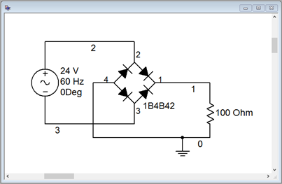
Figure \(\PageIndex{17}\): Simulation schematic for the design of Example \(\PageIndex{1}\) without capacitor.
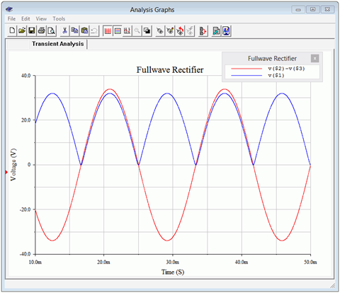
Figure \(\PageIndex{18}\): Transient analysis of the design of Example \(\PageIndex{1}\) without capacitor.
Now that we have confidence in the voltage level and waveform, the output filter capacitor is added as shown in Figure \(\PageIndex{19}\). A transient analysis is run again with the resulting input and load voltage waveforms depicted in Figure \(\PageIndex{20}\). The load voltage is shown in red. The average value is just over 30 volts and the peak-to-peak ripple is less than two volts, as desired. Note that the full-load peak voltage with the capacitor is slightly less than what was seen in the capacitor-less version. If the load current demand were to increase, both droop and ripple would get worse.
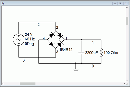
Figure \(\PageIndex{19}\): Simulation schematic for the design of Example \(\PageIndex{1}\) with capacitor.
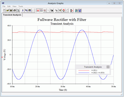
Figure \(\PageIndex{20}\): Transient analysis of the design of Example \(\PageIndex{1}\) with capacitor.
3.2.5: Full-wave Bridge With Dual Outputs
As mentioned, the full-wave bridge can be configured to create a dual output bipolar supply. This is shown in Figure \(\PageIndex{21}\). Note the inclusion of the center tap on the secondary of the transformer and the location of the ground connection between the two loads and their associated capacitors.
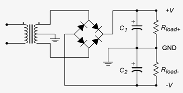
Figure \(\PageIndex{21}\): Dual output full-wave bridge rectifier.
One way of thinking of this is that we have simply created a new reference point, splitting in half the total output potential of the circuit presented in Figure \(\PageIndex{14}\). Alternately, it can be thought of as the upper half of the secondary driving \(R_{load+}\) while the bottom half drives \(R_{load-}\), as if the bridge and two-diode versions were somehow combined in a transporter accident, as in the 1958 movie The Fly, although it doesn't scream “Help me! Help me!” in a tiny little voice at the end.
3.2.6: Zener Regulation
Adding a large capacitor to a rectifier is necessary to store and transfer energy so that a smooth, ideally non-varying voltage results. As noted previously, under heavy load the ripple would increase in amplitude and the average voltage would drop. This issue can be greatly reduced by adding a Zener diode and current limiting resistor to the output, following the capacitor. This is called a Zener regulator and is shown in Figure \(\PageIndex{22}\).
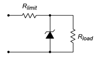
Figure \(\PageIndex{22}\): Simple Zener regulator.
The operation of the Zener regulator is fairly straightforward. Recall that when reverse-biased with a sufficiently large potential, the normal reverse diode behavior of an open switch abruptly changes to maintain a fixed voltage; the Zener potential. The current through the diode begins to increase dramatically once this potential is reached. If we place a Zener diode across the output of our filtered rectifier, the Zener will attempt to limit the output voltage to the Zener potential. To prevent excessive and possibly destructive current draw by the Zener diode, the voltage difference between the capacitor voltage and the Zener potential is dropped across a series current limiting resistor. This limiting resistor will set the maximum amount of output current. This current is then split between the Zener diode and the load. Under light load conditions, most of this current will flow through the Zener diode. Under heavy load conditions, most of the current will be drawn by the load with little flowing through the Zener diode. If the load current demand is too heavy, no current is available for the Zener diode and it stops conducting. Regulation is lost and the limiting resistor forms a voltage divider with the load.
A complete rectifier/filter/Zener regulator circuit is show in Figure \(\PageIndex{22}\). Let's examine how \(R_{limit}\) interacts with the load.
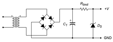
Figure \(\PageIndex{22}\): Full-wave bridge rectifier and filter with Zener regulator.
For proper operation, the Zener potential (\(D_5\)) is the desired DC output voltage and the peak secondary voltage is set somewhat higher. We wish to guarantee that under full load conditions the lowest capacitor voltage due to ripple is still greater than the desired DC output voltage. The difference between the capacitor voltage and the Zener potential drops across \(R_{limit}\). Therefore
\[I = \frac{V_{cap} −V_Z}{R_{limit}} \nonumber \]
Under no-load conditions all of this current flows down through the Zener diode. The maximum load current is equal to this value (at which point no current flows through the Zener diode).
Example \(\PageIndex{2}\)
Determine the maximum load current for a DC supply such as that found in Figure \(\PageIndex{22}\). The capacitor voltage is 15 volts average with \(\pm\)1 volt of ripple (i.e., 16 volts dropping to 14 volts). The Zener potential is 12 volts and \(R_{limit}\) is 4.7 \(\Omega\).
The highest possible continuous load current is the current through \(R_{limit}\) (ignoring \(I_{ZT}\)). The limiting case for continuous draw will occur when the capacitor voltage is at its lowest value, or 14 volts.
\[I = \frac{ V_{cap} −V_Z}{R_{limit}} \nonumber \]
\[I = \frac{14 V −12 V}{4.7 \Omega} \nonumber \]
\[I = 426mA (\text{actually a few mA less due to } I_{ZT} ) \nonumber \]
The highest peak current through the Zener diode is found at the maximum capacitor voltage and assumes no current is drawn by the load.
\[I = \frac{ V_{cap} −V_Z}{R_{limit}} \nonumber \]
\[I = \frac{16 V −12 V}{4.7 \Omega} \nonumber \]
\[I = 851 mA \nonumber \]
Note that this worst case current times the Zener potential results in a power dissipation of about 10 watts. Of course, during normal operation with a load drawing current, the diode dissipation is much reduced. It is interesting to note that the Zener dissipates maximal power when the load current is zero. Consequently, we can think of this circuit as shifting current from the Zener diode to the load as the load demands more current2.
References
1If you're wondering why we don't just use DC distribution instead in order to “cut out the middle man”, the reasons are manifold. First, it is generally more efficient to distribute power via AC rather than DC. Second, even if DC is available, it may not be at the amplitude the circuitry requires. Therefore some form of DC-to-DC conversion would be needed. Depending on the application, this can turn out to be more expensive than AC-to-DC conversion.
2As you might guess, this is not particularly efficient because even when the load demand is nil, the Zener diode is still drawing current from the transformer. An improved circuit may include a bipolar transistor, as examined in Chapter 4. For details on more sophisticated techniques to regulate voltage, see Fiore, J, Operational Amplifiers and Linear Integrated Circuits: Theory and Application, another free OER text.