
3.6: Exercises
- Page ID
- 25401

\( \newcommand{\vecs}[1]{\overset { \scriptstyle \rightharpoonup} {\mathbf{#1}} } \)
\( \newcommand{\vecd}[1]{\overset{-\!-\!\rightharpoonup}{\vphantom{a}\smash {#1}}} \)
\( \newcommand{\id}{\mathrm{id}}\) \( \newcommand{\Span}{\mathrm{span}}\)
( \newcommand{\kernel}{\mathrm{null}\,}\) \( \newcommand{\range}{\mathrm{range}\,}\)
\( \newcommand{\RealPart}{\mathrm{Re}}\) \( \newcommand{\ImaginaryPart}{\mathrm{Im}}\)
\( \newcommand{\Argument}{\mathrm{Arg}}\) \( \newcommand{\norm}[1]{\| #1 \|}\)
\( \newcommand{\inner}[2]{\langle #1, #2 \rangle}\)
\( \newcommand{\Span}{\mathrm{span}}\)
\( \newcommand{\id}{\mathrm{id}}\)
\( \newcommand{\Span}{\mathrm{span}}\)
\( \newcommand{\kernel}{\mathrm{null}\,}\)
\( \newcommand{\range}{\mathrm{range}\,}\)
\( \newcommand{\RealPart}{\mathrm{Re}}\)
\( \newcommand{\ImaginaryPart}{\mathrm{Im}}\)
\( \newcommand{\Argument}{\mathrm{Arg}}\)
\( \newcommand{\norm}[1]{\| #1 \|}\)
\( \newcommand{\inner}[2]{\langle #1, #2 \rangle}\)
\( \newcommand{\Span}{\mathrm{span}}\) \( \newcommand{\AA}{\unicode[.8,0]{x212B}}\)
\( \newcommand{\vectorA}[1]{\vec{#1}} % arrow\)
\( \newcommand{\vectorAt}[1]{\vec{\text{#1}}} % arrow\)
\( \newcommand{\vectorB}[1]{\overset { \scriptstyle \rightharpoonup} {\mathbf{#1}} } \)
\( \newcommand{\vectorC}[1]{\textbf{#1}} \)
\( \newcommand{\vectorD}[1]{\overrightarrow{#1}} \)
\( \newcommand{\vectorDt}[1]{\overrightarrow{\text{#1}}} \)
\( \newcommand{\vectE}[1]{\overset{-\!-\!\rightharpoonup}{\vphantom{a}\smash{\mathbf {#1}}}} \)
\( \newcommand{\vecs}[1]{\overset { \scriptstyle \rightharpoonup} {\mathbf{#1}} } \)
\( \newcommand{\vecd}[1]{\overset{-\!-\!\rightharpoonup}{\vphantom{a}\smash {#1}}} \)
\(\newcommand{\avec}{\mathbf a}\) \(\newcommand{\bvec}{\mathbf b}\) \(\newcommand{\cvec}{\mathbf c}\) \(\newcommand{\dvec}{\mathbf d}\) \(\newcommand{\dtil}{\widetilde{\mathbf d}}\) \(\newcommand{\evec}{\mathbf e}\) \(\newcommand{\fvec}{\mathbf f}\) \(\newcommand{\nvec}{\mathbf n}\) \(\newcommand{\pvec}{\mathbf p}\) \(\newcommand{\qvec}{\mathbf q}\) \(\newcommand{\svec}{\mathbf s}\) \(\newcommand{\tvec}{\mathbf t}\) \(\newcommand{\uvec}{\mathbf u}\) \(\newcommand{\vvec}{\mathbf v}\) \(\newcommand{\wvec}{\mathbf w}\) \(\newcommand{\xvec}{\mathbf x}\) \(\newcommand{\yvec}{\mathbf y}\) \(\newcommand{\zvec}{\mathbf z}\) \(\newcommand{\rvec}{\mathbf r}\) \(\newcommand{\mvec}{\mathbf m}\) \(\newcommand{\zerovec}{\mathbf 0}\) \(\newcommand{\onevec}{\mathbf 1}\) \(\newcommand{\real}{\mathbb R}\) \(\newcommand{\twovec}[2]{\left[\begin{array}{r}#1 \\ #2 \end{array}\right]}\) \(\newcommand{\ctwovec}[2]{\left[\begin{array}{c}#1 \\ #2 \end{array}\right]}\) \(\newcommand{\threevec}[3]{\left[\begin{array}{r}#1 \\ #2 \\ #3 \end{array}\right]}\) \(\newcommand{\cthreevec}[3]{\left[\begin{array}{c}#1 \\ #2 \\ #3 \end{array}\right]}\) \(\newcommand{\fourvec}[4]{\left[\begin{array}{r}#1 \\ #2 \\ #3 \\ #4 \end{array}\right]}\) \(\newcommand{\cfourvec}[4]{\left[\begin{array}{c}#1 \\ #2 \\ #3 \\ #4 \end{array}\right]}\) \(\newcommand{\fivevec}[5]{\left[\begin{array}{r}#1 \\ #2 \\ #3 \\ #4 \\ #5 \\ \end{array}\right]}\) \(\newcommand{\cfivevec}[5]{\left[\begin{array}{c}#1 \\ #2 \\ #3 \\ #4 \\ #5 \\ \end{array}\right]}\) \(\newcommand{\mattwo}[4]{\left[\begin{array}{rr}#1 \amp #2 \\ #3 \amp #4 \\ \end{array}\right]}\) \(\newcommand{\laspan}[1]{\text{Span}\{#1\}}\) \(\newcommand{\bcal}{\cal B}\) \(\newcommand{\ccal}{\cal C}\) \(\newcommand{\scal}{\cal S}\) \(\newcommand{\wcal}{\cal W}\) \(\newcommand{\ecal}{\cal E}\) \(\newcommand{\coords}[2]{\left\{#1\right\}_{#2}}\) \(\newcommand{\gray}[1]{\color{gray}{#1}}\) \(\newcommand{\lgray}[1]{\color{lightgray}{#1}}\) \(\newcommand{\rank}{\operatorname{rank}}\) \(\newcommand{\row}{\text{Row}}\) \(\newcommand{\col}{\text{Col}}\) \(\renewcommand{\row}{\text{Row}}\) \(\newcommand{\nul}{\text{Nul}}\) \(\newcommand{\var}{\text{Var}}\) \(\newcommand{\corr}{\text{corr}}\) \(\newcommand{\len}[1]{\left|#1\right|}\) \(\newcommand{\bbar}{\overline{\bvec}}\) \(\newcommand{\bhat}{\widehat{\bvec}}\) \(\newcommand{\bperp}{\bvec^\perp}\) \(\newcommand{\xhat}{\widehat{\xvec}}\) \(\newcommand{\vhat}{\widehat{\vvec}}\) \(\newcommand{\uhat}{\widehat{\uvec}}\) \(\newcommand{\what}{\widehat{\wvec}}\) \(\newcommand{\Sighat}{\widehat{\Sigma}}\) \(\newcommand{\lt}{<}\) \(\newcommand{\gt}{>}\) \(\newcommand{\amp}{&}\) \(\definecolor{fillinmathshade}{gray}{0.9}\)(Assume diodes are silicon unless stated otherwise)
3.6.1: Analysis Problems
1. For the circuit of Figure \(\PageIndex{1}\), determine the peak output voltage. \(V_{sec} = 12\) volts RMS, \(R_{load} = 50\) \(\Omega\), \(C_1 = 1500\) \(\mu\)F.
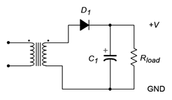
Figure \(\PageIndex{1}\)
2. Sketch the output voltage waveform for the circuit of Problem 1, Figure \(\PageIndex{1}\), with and without the capacitor.
3. Determine the peak output voltage for the circuit of Figure \(\PageIndex{2}\). \(V_{sec} = 18\) volts RMS, \(R_{load} = 75\) \(\Omega\), \(C_1 = 470\) \(\mu\)F.
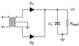
Figure \(\PageIndex{2}\)
4. Sketch the output voltage waveform for the circuit of Problem 3, Figure \(\PageIndex{2}\), with and without the capacitor.
5. For the circuit of Figure \(\PageIndex{3}\), determine the peak output voltage. \(V_{sec} = 18\) volts RMS, \(R_{load} = 40\) \(\Omega\), \(C_1 = 1000\) \(\mu\)F.
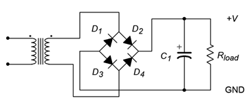
Figure \(\PageIndex{3}\)
6. Sketch the output voltage waveform for the circuit of Problem 5, Figure \(\PageIndex{3}\), with and without the capacitor.
7. Determine the output voltage waveform and its amplitude for the circuit of Figure \(\PageIndex{4}\). \(V_{in} = 10 \sin 2\pi 100t\), \(V_{clip} = 8\) volts, \(R = 10\) k\(\Omega\).
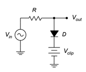
Figure \(\PageIndex{4}\)
8. Draw the output waveform with its amplitudes for the circuit of Figure \(\PageIndex{5}\). \(V_{in} = 10 \sin 2\pi 100t\), \(V_{clip} = 5\) volts, \(R = 10\) k\(\Omega\).
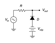
Figure \(\PageIndex{5}\)
9. Draw the output waveform with its amplitudes for the circuit of Figure \(\PageIndex{6}\). \(V_{in} = 12 \sin 2\pi 200t\), \(V_1 = 6\) volts, \(V_2 = 4\) volts, \(R = 10\) k\(\Omega\).
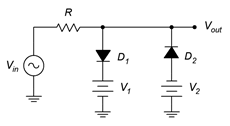
Figure \(\PageIndex{6}\)
10. Draw the output waveform with its amplitudes for the circuit of Figure \(\PageIndex{7}\). \(V_{in} = 5 \sin 2\pi 2000t\), \(C = 10\) \(\mu\)F, \(R = 4.7\) k\(\Omega\).
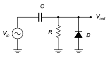
Figure \(\PageIndex{7}\)
11. Draw the output waveform with its amplitudes for the circuit of Figure \(\PageIndex{8}\). \(V_{in} = 8 \sin 2\pi 500t\), \(V_{clamp} = 2\) volts, \(C = 4.7\) \(\mu\)F, \(R = 33\) k\(\Omega\).
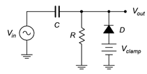
Figure \(\PageIndex{8}\)
3.6.2: Design Problems
12. Design a 15 volt AC to DC power supply capable of drawing 200 mA.
13. Design a circuit that will limit its output voltage to a range of −5 volts to +10 volts.
14. Design a circuit that will shift its output voltage so that it is always positive. The input frequency is 2 kHz.
3.6.3: Challenge Problems
15. Design a circuit that will shift its output voltage so that its negative peak is at +3 volts. The input frequency range is from 100 Hz to 1 kHz.
3.6.4: Computer Simulation Problems
16. Run a transient analysis of the circuit in Figure \(\PageIndex{1}\), Problem 1.
17. Run a transient analysis of the circuit in Figure \(\PageIndex{2}\), Problem 3.
18. Run a transient analysis of the circuit in Figure \(\PageIndex{3}\), Problem 5.
19. Run two transient analyses on the clamper circuit of Example 3.4.1, first using a capacitor 100 times larger than specified, and second using a capacitor 100 times smaller than specified. Discuss the resulting waveforms.